High-Speed M Series Multifunction DAQ
16-Bit, up to 1.25 MS/s, up to 32 Analog Inputs
NEW
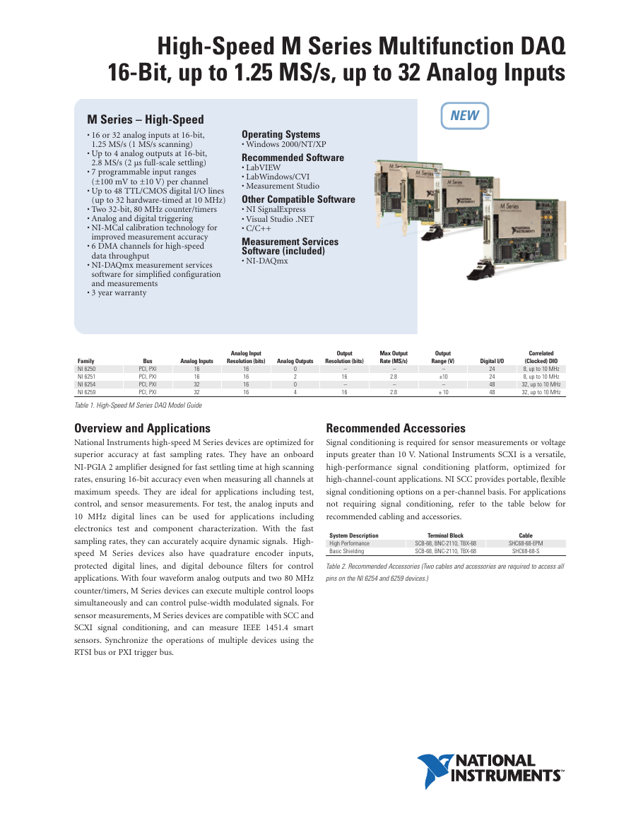
M Series – High-Speed
• 16 or 32 analog inputs at 16-bit,
1.25 MS/s (1 MS/s scanning)
• Up to 4 analog outputs at 16-bit,
2.8 MS/s (2 µs full-scale settling)
• 7 programmable input ranges
(±100 mV to ±10 V) per channel
• Up to 48 TTL/CMOS digital I/O lines
(up to 32 hardware-timed at 10 MHz)
• Two 32-bit, 80 MHz counter/timers
• Analog and digital triggering
• NI-MCal calibration technology for
improved measurement accuracy
• 6 DMA channels for high-speed
data throughput
• NI-DAQmx measurement services
software for simplified configuration
and measurements
• 3 year warranty
Operating Systems
• Windows 2000/NT/XP
Recommended Software
• LabVIEW
• LabWindows/CVI
• Measurement Studio
Other Compatible Software
• NI SignalExpress
• Visual Studio .NET
• C/C++
Measurement Services
Software (included)
• NI-DAQmx
Family
NI 6250
NI 6251
NI 6254
NI 6259
Bus
PCI, PXI
PCI, PXI
PCI, PXI
PCI, PXI
Analog Inputs
Analog Input
Resolution (bits)
Analog Outputs
Resolution (bits)
Output
Max Output
Rate (MS/s)
Output
Range (V)
Digital I/O
16
16
32
32
16
16
16
16
0
2
0
4
–
16
–
16
–
2.8
–
2.8
–
±10
–
± 10
24
24
48
48
Correlated
(Clocked) DIO
8, up to 10 MHz
8, up to 10 MHz
32, up to 10 MHz
32, up to 10 MHz
Table 1. High-Speed M Series DAQ Model Guide
Overview and Applications
National Instruments high-speed M Series devices are optimized for
superior accuracy at fast sampling rates. They have an onboard
NI-PGIA 2 amplifier designed for fast settling time at high scanning
rates, ensuring 16-bit accuracy even when measuring all channels at
maximum speeds. They are ideal for applications including test,
control, and sensor measurements. For test, the analog inputs and
10 MHz digital lines can be used for applications including
electronics test and component characterization. With the fast
sampling rates, they can accurately acquire dynamic signals. High-
speed M Series devices also have quadrature encoder inputs,
protected digital lines, and digital debounce filters for control
applications. With four waveform analog outputs and two 80 MHz
counter/timers, M Series devices can execute multiple control loops
simultaneously and can control pulse-width modulated signals. For
sensor measurements, M Series devices are compatible with SCC and
SCXI signal conditioning, and can measure IEEE 1451.4 smart
sensors. Synchronize the operations of multiple devices using the
RTSI bus or PXI trigger bus.
Recommended Accessories
Signal conditioning is required for sensor measurements or voltage
inputs greater than 10 V. National Instruments SCXI is a versatile,
high-performance signal conditioning platform, optimized for
high-channel-count applications. NI SCC provides portable, flexible
signal conditioning options on a per-channel basis. For applications
not requiring signal conditioning, refer to the table below for
recommended cabling and accessories.
System Description
High Performance
Basic Shielding
Terminal Block
SCB-68, BNC-2110, TBX-68
SCB-68, BNC-2110, TBX-68
Cable
SHC68-68-EPM
SHC68-68-S
Table 2. Recommended Accessories (Two cables and accessories are required to access all
pins on the NI 6254 and 6259 devices.)
�
High-Speed M Series Multifunction DAQ
16-Bit, up to 1.25 MS/s, up to 32 Analog Inputs
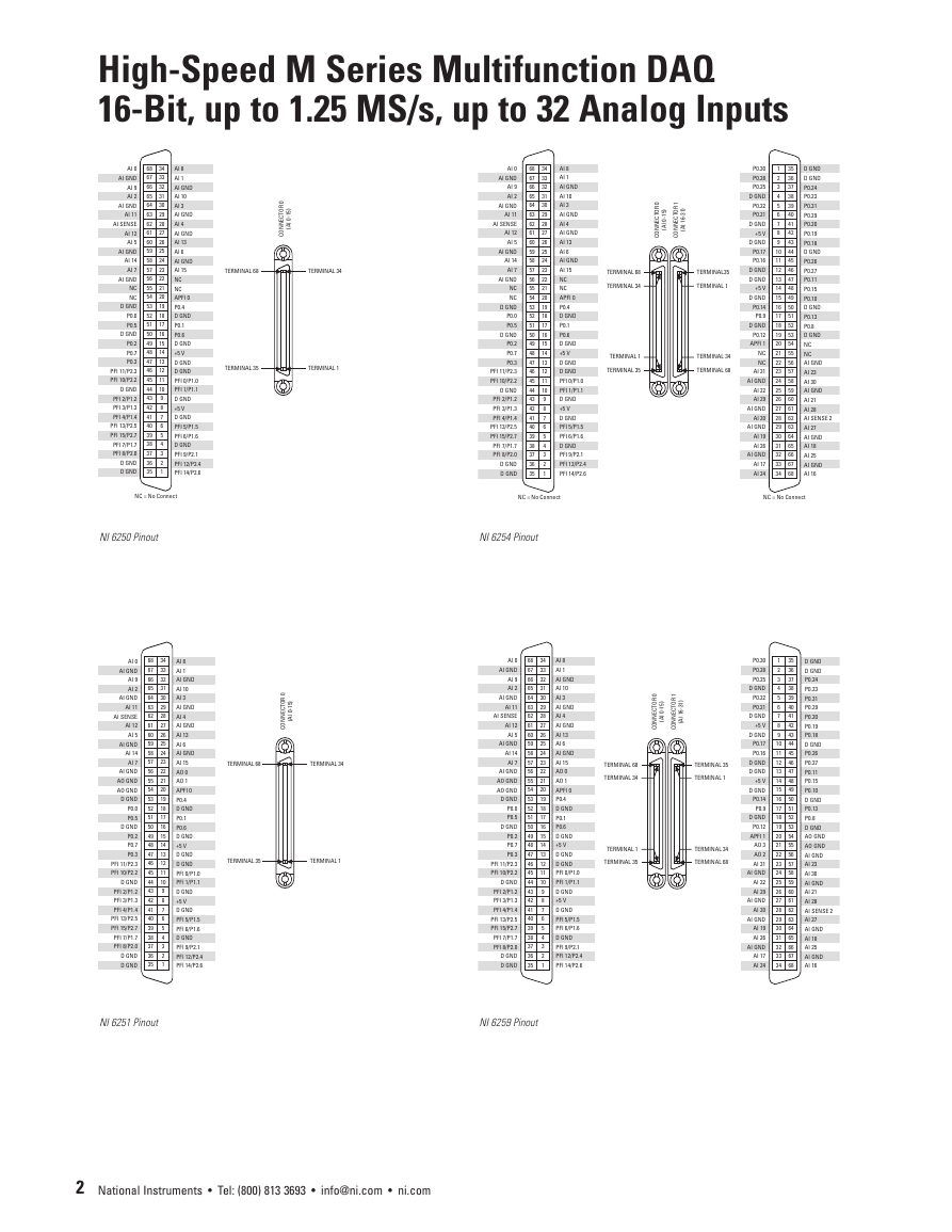
NI 6250 Pinout
NI 6254 Pinout
NI 6251 Pinout
NI 6259 Pinout
2 National Instruments • Tel: (800) 813 3693 • info@ni.com • ni.com
CONNECTOR 0(AI 0-15)TERMINAL 34TERMINAL 68TERMINAL 1TERMINAL 35D GNDD GNDPFI 8/P2.0PFI 7/P1.7PFI 15/P2.7PFI 13/P2.5PFI 4/P1.4PFI 3/P1.3PFI 2/P1.2D GNDPFI 10/P2.2PFI 11/P2.3P0.3P0.7P0.2D GNDP0.5P0.0D GNDNCNCAI GNDAI 7AI 14AI GNDAI 5AI 12AI SENSEAI 11AI GNDAI 2AI 9AI GNDAI 0PFI 14/P2.6PFI 9/P2.1D GNDPFI 5/P1.5D GND+5 VD GNDPFI 12/P2.4PFI 6/P1.6PFI 1/P1.1PFI 0/P1.0D GNDD GND+5 VD GNDP0.6P0.1D GNDP0.4APFI 0NCNCAI 15AI GNDAI 6AI 13AI GNDAI 4AI GNDAI 3AI 10AI GNDAI 1AI 86834673366326531643063296228612760265925582457235622552154205319521851175016491548144713461245114410439428417406395384373362351NC = No ConnectCONNECTOR 0(AI 0-15)D GNDD GNDPFI 8/P2.0PFI 7/P1.7PFI 15/P2.7PFI 13/P2.5PFI 4/P1.4PFI 3/P1.3PFI 2/P1.2D GNDPFI 10/P2.2PFI 11/P2.3P0.3P0.7P0.2D GNDP0.5P0.0D GNDAO GNDAO GNDAI GNDAI 7AI 14AI GNDAI 5AI 12AI SENSEAI 11AI GNDAI 2AI 9AI GNDAI 0PFI 14/P2.6PFI 9/P2.1D GNDPFI 5/P1.5D GND+5 VD GNDPFI 12/P2.4PFI 6/P1.6PFI 1/P1.1PFI 0/P1.0D GNDD GND+5 VD GNDP0.6P0.1D GNDP0.4APFI 0AO 1AO 0 AI 15AI GNDAI 6AI 13AI GNDAI 4AI GNDAI 3AI 10AI GNDAI 1AI 86834673366326531643063296228612760265925582457235622552154205319521851175016491548144713461245114410439428417406395384373362351TERMINAL 34TERMINAL 68TERMINAL 1TERMINAL 35CONNECTOR 0(AI 0-15)CONNECTOR 1(AI 16-31)TERMINAL 34TERMINAL 68TERMINAL 35TERMINAL 1TERMINAL35TERMINAL 1TERMINAL 34TERMINAL 68D GNDD GNDPFI 8/P2.0PFI 7/P1.7PFI 15/P2.7PFI 13/P2.5PFI 4/P1.4PFI 3/P1.3PFI 2/P1.2D GNDPFI 10/P2.2PFI 11/P2.3P0.3P0.7P0.2D GNDP0.5P0.0D GNDNCNCAI GNDAI 7AI 14AI GNDAI 5AI 12AI SENSEAI 11AI GNDAI 2AI 9AI GNDAI 0PFI 14/P2.6PFI 9/P2.1D GNDPFI 5/P1.5D GND+5 VD GNDPFI 12/P2.4PFI 6/P1.6PFI 1/P1.1PFI 0/P1.0D GNDD GND+5 VD GNDP0.6P0.1D GNDP0.4APFI 0NCNCAI 15AI GNDAI 6AI 13AI GNDAI 4AI GNDAI 3AI 10AI GNDAI 1AI 86834673366326531643063296228612760265925582457235622552154205319521851175016491548144713461245114410439428417406395384373362351NC = No ConnectAI 24AI 17AI GNDAI 26AI 19AI GNDAI 20AI GNDAI 29AI 22AI GNDAI 31NCNCAPFI 1P0.12D GNDP0.9P0.14D GND+5 VD GNDD GNDP0.16P0.17D GND+5 VD GNDP0.21P0.22D GNDP0.25P0.28P0.30AI 16AI 25AI 18AI 27AI SENSE 2AI 28AI 21AI GNDAI GNDAI GNDAI 30AI 23AI GNDNCNCD GNDP0.8P0.13D GNDP0.10P0.15P0.11 P0.27P0.26D GNDP0.18P0.19P0.20P0.29P0.31P0.23P0.24D GNDD GND1352363374385396407418429431044114512461347144815491650175118521953205421552256235724582559266027612862296330643165326633673468NC = No ConnectCONNECTOR 0(AI 0-15)CONNECTOR 1(AI 16-31)AI 24AI 17AI GNDAI 26AI 19AI GNDAI 20AI GNDAI 29AI 22AI GNDAI 31AO 2AO 3APFI 1P0.12D GNDP0.9P0.14D GND+5 VD GNDD GNDP0.16P0.17D GND+5 VD GNDP0.21P0.22D GNDP0.25P0.28P0.30AI 16AI 25AI 18AI 27AI SENSE 2AI 28AI 21AI GNDAI GNDAI GNDAI 30AI 23AI GNDAO GNDAO GNDD GNDP0.8P0.13D GNDP0.10P0.15P0.11 P0.27P0.26D GNDP0.18P0.19P0.20P0.29P0.31P0.23P0.24D GNDD GND1352363374385396407418429431044114512461347144815491650175118521953205421552256235724582559266027612862296330643165326633673468D GNDD GNDPFI 8/P2.0PFI 7/P1.7PFI 15/P2.7PFI 13/P2.5PFI 4/P1.4PFI 3/P1.3PFI 2/P1.2D GNDPFI 10/P2.2PFI 11/P2.3P0.3P0.7P0.2D GNDP0.5P0.0D GNDAO GNDAO GNDAI GNDAI 7AI 14AI GNDAI 5AI 12AI SENSEAI 11AI GNDAI 2AI 9AI GNDAI 0PFI 14/P2.6PFI 9/P2.1D GNDPFI 5/P1.5D GND+5 VD GNDPFI 12/P2.4PFI 6/P1.6PFI 1/P1.1PFI 0/P1.0D GNDD GND+5 VD GNDP0.6P0.1D GNDP0.4APFI 0AO 1AO 0 AI 15AI GNDAI 6AI 13AI GNDAI 4AI GNDAI 3AI 10AI GNDAI 1AI 86834673366326531643063296228612760265925582457235622552154205319521851175016491548144713461245114410439428417406395384373362351TERMINAL 34TERMINAL 68TERMINAL 35TERMINAL 1TERMINAL 35TERMINAL 1TERMINAL 34TERMINAL 68�
High-Speed M Series Multifunction DAQ
16-Bit, up to 1.25 MS/s, up to 32 Analog Inputs
BUY ONLINE!
For complete product specifications, pricing, and accessory
information, call (800) 813-3693 (U.S. only) or go to ni.com/daq.
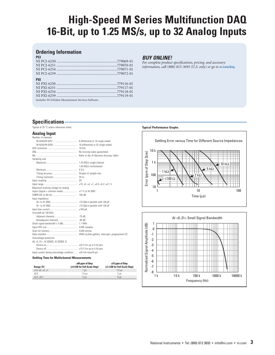
Typical Performance Graphs
Ordering Information
PCI
NI PCI-6250 ..................................................................779069-01
NI PCI-6251 ..................................................................779070-01
NI PCI-6254 ..................................................................779071-01
NI PCI-6259 ..................................................................779072-01
PXI
NI PXI-6250 ..................................................................779116-01
NI PXI-6251 ..................................................................779117-01
NI PXI-6254 ..................................................................779118-01
NI PXI-6259 ..................................................................779119-01
Includes NI-DAQmx Measurement Services Software.
Specifications
Typical at 25 °C unless otherwise noted.
Analog Input
Number of channels
NI 6250/NI 6251........................................ 8 differential or 16 single ended
NI 6254/NI 6259........................................ 16 differential or 32 single ended
ADC resolution ................................................. 16 bits
DNL................................................................... No missing codes guaranteed
INL ................................................................... Refer to the AI Absolute Accuracy Table
Sampling rate
Maximum................................................... 1.25 MS/s single-channel
1.00 MS/s multichannel
Minimum.................................................... 0 S/s
Timing accuracy......................................... 50 ppm of sample rate
Timing resolution....................................... 50 ns
Input coupling................................................... DC
Input range ....................................................... ±10, ±5, ±2, ±1, ±0.5, ±0.2, ±0.1 V
Maximum working voltage for analog
inputs (signal + common mode)....................... ±11 V of AI GND
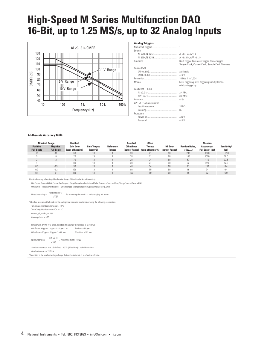
CMRR (DC to 60 Hz) ......................................... 100 dB
Input impedance
AI+ to AI GND............................................ >10 GΩ in parallel with 100 pF
AI– to AI GND............................................ >10 GΩ in parallel with 100 pF
Input bias current ............................................. ±100 pA
Crosstalk (at 100 kHz)
Adjacent channels.....................................
Nonadjacent channels...............................
-75 dB
-95 dB
Small signal bandwidth (–3 dB)....................... 1.7 MHz
Input FIFO size .................................................. 4,095 samples
Scan list memory.............................................. 4,095 entries
Data transfers .................................................. DMA (scatter-gather), interrupts, programmed I/O
Overvoltage protection
(AI <0..31>, AI SENSE, AI SENSE 2)
Device on................................................... ±25 V for up to 4 AI pins
Device off .................................................. ±15 V for up to 4 AI pins
Input current during overvoltage condition ..... ±20 mA max/AI pin
Settling Time for Multichannel Measurements
Range (V)
±10, ±5, ±2, ±1
±0.5
±0.2, ±0.1
±60 ppm of Step
±15 ppm of Step
(±4 LSB for Full Scale Step)
(±1 LSB for Full Scale Step)
1 µs
1.5 µs
2 µs
1.5 µs
2 µs
8 µs
National Instruments • Tel: (800) 813 3693 • info@ni.com • ni.com
3
Settling Error versus Time for Different Source Impedances101001 k10 k110100Time (µs)Error(ppmofStepSize)5 kΩ10 kΩ2 kΩ1 kΩ≤100 ΩAI <0..31> Small Signal Bandwidth-8-7-6-5-4-3-2-1011 k10 k100 k1000 k10000 kFrequency (Hz)Normalized Signal Amplitude (dB)�
High-Speed M Series Multifunction DAQ
16-Bit, up to 1.25 MS/s, up to 32 Analog Inputs
Analog Triggers
Number of triggers........................................... 1
Source
NI 6250/NI 6251........................................ AI <0..15>, APFI 0
NI 6254/NI 6259........................................ AI <0..31>, APFI <0..1>
Functions .......................................................... Start Trigger, Reference Trigger, Pause Trigger,
Sample Clock, Convert Clock, Sample Clock Timebase
Source level
(AI <0..31>) ................................................ ±full scale
(APFI <0..1>)............................................... ±10 V
Resolution......................................................... 10 bits, 1 in 1,024
Modes ............................................................
Level triggering, level triggering with hysteresis,
window triggering
Bandwidth (–3 dB)
AI <0..31> .................................................. 3.4 MHz
APFI <0..1>................................................. 3.9 MHz
Accuracy ........................................................... ±1%
APFI <0..1> characteristics
Input impedance........................................ 10 kΩ
Coupling..................................................... DC
Protection
Power on.................................................... ±30 V
Power off ................................................... ±15 V
Absolute
Accuracy at
Full Scale1 (µV)
1920
1010
410
220
130
74
52
Sensitivity2
(µV)
112.0
56.0
22.8
12.8
8.4
6.4
6.0
σ (µVrms)
280
140
57
32
21
16
15
AI Absolute Accuracy Table
Nominal Range
Positive
Full Scale
Negative
Full Scale
Residual
Gain Error
(ppm of Reading)
Gain Tempco
(ppm/°C)
Reference
Tempco
Residual
Offset Error
Offset
Tempco
INL Error
Random Noise,
(ppm of Range)
(ppm of Range/°C)
(ppm of Range)
10
5
2
1
0.5
0.2
0.1
-10
-5
-2
-1
-0.5
-0.2
-0.1
60
70
70
80
90
130
150
13
13
13
13
13
13
13
1
1
1
1
1
1
1
20
20
20
20
40
80
150
21
21
24
27
34
55
90
60
60
60
60
60
60
60
AbsoluteAccuracy = Reading · (GainError) + Range · (OffsetError) + NoiseUncertainty
GainError = ResidualAIGainError + GainTempco · (TempChangeFromLastInternalCal) + ReferenceTempco · (TempChangeFromLastExternalCal)
OffsetError = ResidualAIOffsetError + OffsetTempco · (TempChangeFromLastInternalCal) + INL_Error
NoiseUncertainty =
RandomNoise · 3
,
√100
For a coverage factor of 3 σ and averaging 100 points
1 Absolute accuracy at full scale on the analog input channels is determined using the following assumptions:
TempChangeFromLastExternalCal = 10 °C
TempChangeFromLastInternalCal = 1 °C
number_of_readings = 100
CoverageFactor = 3 σ
For example, on the 10 V range, the absolute accuracy at full scale is as follows:
GainError = 60 ppm + 13 ppm · 1 + 1 ppm · 10
OffsetError = 20 ppm + 21 ppm · 1 + 60 ppm
GainError = 83 ppm
OffsetError = 101 ppm
NoiseUncertainty =
275 µV · 3
√100
,
NoiseUncertainty = 83 µV
AbsoluteAccuracy = 10 V · (GainError) + 10 V · (OffsetError) + NoiseUncertainty
AbsoluteAccuracy = 1920 µV
2 Sensitivity is the smallest voltage change that can be detected. It is a function of noise.
4 National Instruments • Tel: (800) 813 3693 • info@ni.com • ni.com
AI<0. .31> CMRR405060708090100110120130101001 k10 k100 kFrequency (Hz)CMRR (dB)10 V Range5 V Range0.1 V Range�
High-Speed M Series Multifunction DAQ
16-Bit, up to 1.25 MS/s, up to 32 Analog Inputs
Analog Output
Number of channels
NI 6250 ...................................................... 0
NI 6251 ...................................................... 2
NI 6254 ...................................................... 0
NI 6259 ...................................................... 4
DAC resolution ................................................. 16 bits
DNL................................................................... ±1 LSB
Monotonicity .................................................... 16 bit guaranteed
Accuracy ........................................................... Refer to the AO Absolute Accuracy Table
Maximum update rate
1 channel ................................................... 2.86 MS/s
2 channels ................................................. 2.00 MS/s
3 channels ................................................. 1.54 MS/s
4 channels ................................................. 1.25 MS/s
Timing accuracy................................................ 50 ppm of sample rate
Timing resolution.............................................. 50 ns
Output range .................................................... ±10 V, ±5 V, ±external reference on APFI <0..1>
Output coupling................................................ DC
Output impedance............................................ 0.2 Ω
Output current drive ......................................... ±5 mA
Overdrive protection......................................... ±25 V
Overdrive current.............................................. 20 mA
Power-on state ................................................. ±5 mV
Power-on glitch ................................................ 1.5 V peak for 1.5 s
Output FIFO size ............................................... 8,191 samples shared among channels used
Data transfers .................................................. DMA (scatter-gather), interrupts, programmed I/O
AO waveform modes:
• Non-periodic waveform
• Periodic waveform regeneration mode from onboard FIFO
• Periodic waveform regeneration from host buffer including dynamic update
Settling time, full scale step
15 ppm (1 LSB) ................................................. 2 µs
Slew rate.......................................................... 20 V/µs
Glitch energy at midscale transition, ±10 V range
Magnitude ................................................. 10 mV
Duration ..................................................... 1 µs
AO Absolute Accuracy Table
Nominal Range
Positive
Full Scale
10
5
Negative
Full Scale
-10
-5
Residual
Gain Error
(ppm of Reading)
75
85
Gain Tempco
(ppm/°C)
17
8
Reference
Tempco
1
1
Residual
Offset Error
(ppm of Range)
40
40
Offset Tempco
(ppm of Range/°C)
INL Error
(ppm of Range)
2
2
64
64
Absolute
Accuracy at
Full Scale1 (µV)
2080
1045
1 Absolute Accuracy at full scale numbers is valid immediately following internal calibration and assume the device is operating within 10 °C of the last external calibration.
AbsoluteAccuracy = OutputValue · (GainError) + Range · (OffsetError)
GainError = ResidualGainError + GainTempco · (TempChangeFromLastInternalCal) + ReferenceTempco · (TempChangeFromLastExternalCal)
OffsetError = ResidualOffsetError + AOOffsetTempco · (TempChangeFromLastInternalCal) + INL_Error
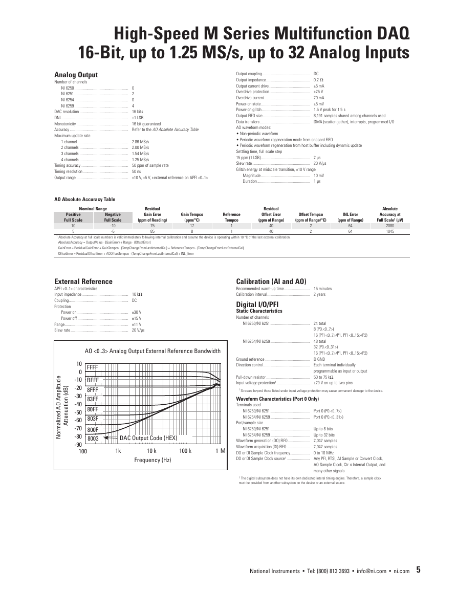
External Reference
APFI <0..1> characteristics
Input impedance............................................... 10 kΩ
Coupling............................................................ DC
Protection
Power on.................................................... ±30 V
Power off ................................................... ±15 V
Range................................................................ ±11 V
Slew rate.......................................................... 20 V/µs
Calibration (AI and AO)
Recommended warm-up time.......................... 15 minutes
Calibration interval........................................... 2 years
Digital I/O/PFI
Static Characteristics
Number of channels
NI 6250/NI 6251........................................ 24 total
NI 6254/NI 6259........................................ 48 total
8 (P0.<0..7>)
16 (PFI <0..7>/P1, PFI <8..15>/P2)
32 (P0.<0..31>)
16 (PFI <0..7>/P1, PFI <8..15>/P2)
Ground reference ............................................. D GND
Direction control............................................... Each terminal individually
programmable as input or output
Pull-down resistor ............................................ 50 to 75 kΩ
Input voltage protection1 ................................. ±20 V on up to two pins
1 Stresses beyond those listed under input voltage protection may cause permanent damage to the device.
Waveform Characteristics (Port 0 Only)
Terminals used
NI 6250/NI 6251........................................ Port 0 (P0.<0..7>)
NI 6254/NI 6259........................................ Port 0 (P0.<0..31>)
Port/sample size
NI 6250/NI 6251........................................ Up to 8 bits
NI 6254/NI 6259........................................ Up to 32 bits
Waveform generation (DO) FIFO ...................... 2,047 samples
Waveform acquisition (DI) FIFO ....................... 2,047 samples
DO or DI Sample Clock frequency.................... 0 to 10 MHz
DO or DI Sample Clock source1 ....................... Any PFI, RTSI, AI Sample or Convert Clock,
AO Sample Clock, Ctr n Internal Output, and
many other signals
1 The digital subsystem does not have its own dedicated interal timing engine. Therefore, a sample clock
must be provided from another subsystem on the device or an external source.
National Instruments • Tel: (800) 813 3693 • info@ni.com • ni.com
5
AO <0..3> Analog Output External Reference Bandwidth-90-80-70-60-50-40-30-20-10010100 1k10 k100 k1 MFrequency (Hz)Normalized AO AmplitudeAttenuation (dB)DAC Output Code (HEX)8003800F803F80FF83FF8FFFBFFFFFFF�
High-Speed M Series Multifunction DAQ
16-Bit, up to 1.25 MS/s, up to 32 Analog Inputs
PFI/Port 1/Port 2 Functionality
Functionality ..................................................... Static digital input, static digital
output, timing input, timing output
Timing output sources...................................... Many AI, AO, counter, DI, DO timing signals
Debounce filter settings................................... 125 ns, 6.425 µs, 2.54 ms, disable; high
and low transitions; selectable per input
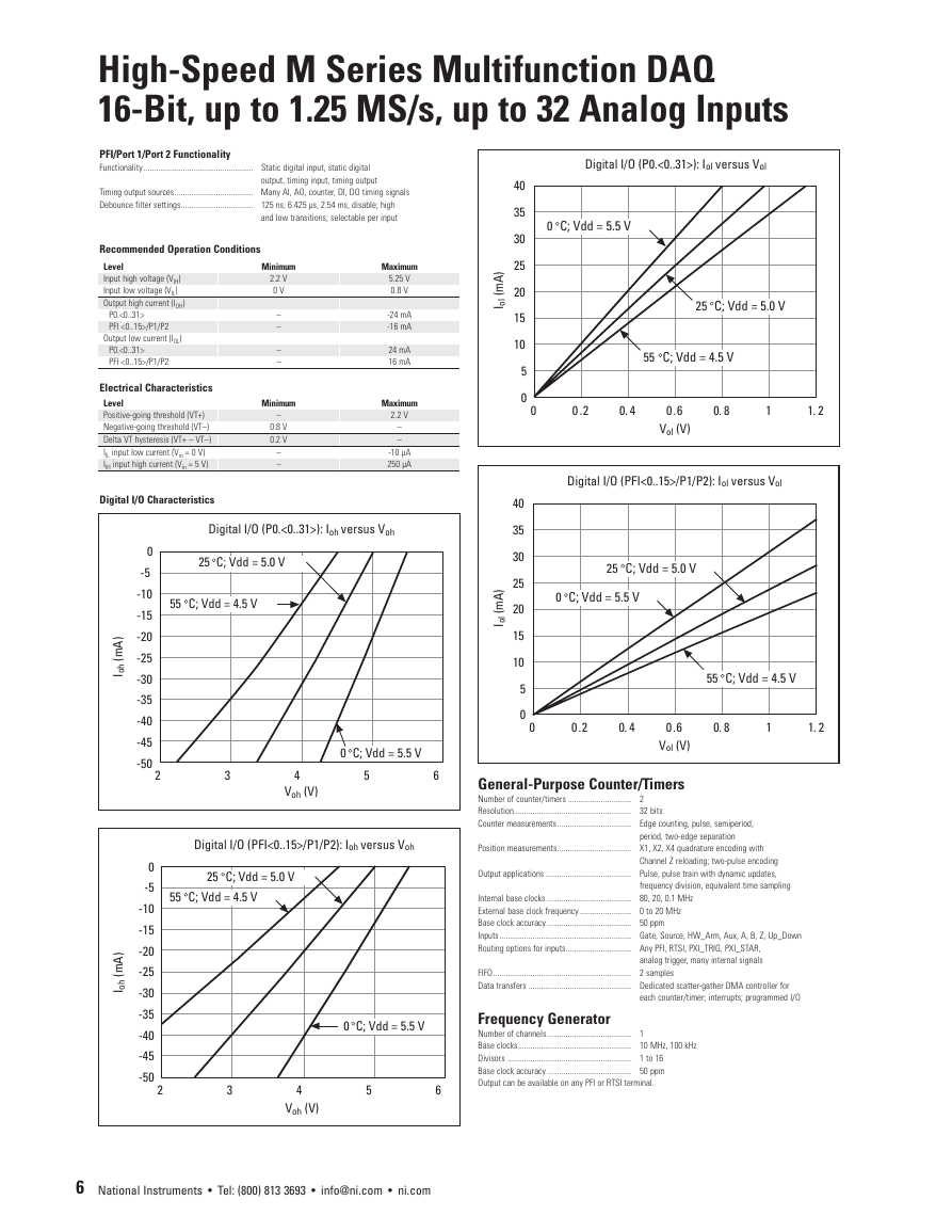
Recommended Operation Conditions
Level
Input high voltage (VIH)
Input low voltage (VIL)
Output high current (IOH)
P0.<0..31>
PFI <0..15>/P1/P2
Output low current (IOL)
P0.<0..31>
PFI <0..15>/P1/P2
Minimum
2.2 V
0 V
–
–
–
–
Electrical Characteristics
Level
Positive-going threshold (VT+)
Negative-going threshold (VT–)
Delta VT hysteresis (VT+ – VT–)
IIL input low current (Vin = 0 V)
IIH input high current (Vin = 5 V)
Digital I/O Characteristics
Minimum
–
0.8 V
0.2 V
–
–
Maximum
5.25 V
0.8 V
-24 mA
-16 mA
24 mA
16 mA
Maximum
2.2 V
–
–
-10 µA
250 µA
General-Purpose Counter/Timers
Number of counter/timers ............................... 2
Resolution......................................................... 32 bits
Counter measurements.................................... Edge counting, pulse, semiperiod,
period, two-edge separation
Position measurements.................................... X1, X2, X4 quadrature encoding with
Channel Z reloading; two-pulse encoding
Output applications.......................................... Pulse, pulse train with dynamic updates,
frequency division, equivalent time sampling
Internal base clocks ......................................... 80, 20, 0.1 MHz
External base clock frequency ......................... 0 to 20 MHz
Base clock accuracy ......................................... 50 ppm
Inputs................................................................ Gate, Source, HW_Arm, Aux, A, B, Z, Up_Down
Routing options for inputs................................ Any PFI, RTSI, PXI_TRIG, PXI_STAR,
analog trigger, many internal signals
FIFO................................................................... 2 samples
Data transfers .................................................. Dedicated scatter-gather DMA controller for
each counter/timer; interrupts; programmed I/O
Frequency Generator
Number of channels......................................... 1
Base clocks....................................................... 10 MHz, 100 kHz
Divisors ............................................................ 1 to 16
Base clock accuracy ......................................... 50 ppm
Output can be available on any PFI or RTSI terminal.
6 National Instruments • Tel: (800) 813 3693 • info@ni.com • ni.com
051015202530354000.20.40.60.811.2Vol (V)Iol (mA)Digital I/O (P0.<0..31>): Iol versus Vol0 C; Vdd = 5.5 V55 C; Vdd = 4.5 V25 C; Vdd = 5.0 V051015202530354000.20.40.60.811.2Vol (V)Iol(mA)Digital I/O (PFI<0..15>/P1/P2): Iol versus Vol0 C; Vdd = 5.5 V55 C; Vdd = 4.5 V25 C; Vdd = 5.0 V-50-45-40-35-30-25-20-15-10-5023456Voh (V)Ioh (mA)0 C; Vdd = 5.5 V55 C; Vdd = 4.5 V25 C; Vdd = 5.0 VDigital I/O (P0.<0..31>): Iohversus Voh-50-45-40-35-30-25-20-15-10-5023456Voh (V)Ioh (mA)Digital I/O (PFI<0..15>/P1/P2): Iohversus Voh0 C; Vdd = 5.5 V55 C; Vdd = 4.5 V25 C; Vdd = 5.0 V�
High-Speed M Series Multifunction DAQ
16-Bit, up to 1.25 MS/s, up to 32 Analog Inputs
Phase-Locked Loop (PLL)
Number of PLLs ................................................ 1
Reference signal .............................................. PXI_STAR, PXI_CLK10, RTSI <0..7>
Output of PLL.................................................... 80 MHz Timebase; other signals derived from 80 MHz
Physical
Dimensions
PCI.............................................................. 9.7 cm by 15.5 cm (3.8 in. by 6.1 in.)
PXI.............................................................. Standard 3U PXI
Timebase including 20 MHz and 100 kHz Timebases
I/O connectors
External Digital Triggers
Source............................................................... Any PFI, RTSI, PXI_TRIG, PXI_STAR
Polarity ............................................................ Software-selectable for most signals
Analog input function....................................... Start Trigger, Reference Trigger, Pause Trigger,
Sample Clock, Convert Clock, Sample Clock Timebase
Analog output function .................................... Start Trigger, Pause Trigger, Sample
Clock, Sample Clock Timebase
Counter/timer functions................................... Gate, Source, HW_Arm, Aux, A, B, Z, Up_Down
Digital waveform generation (DO) function ...... Sample Clock
Digital waveform acquisition (DI) function........ Sample Clock
Device-To-Device Trigger Bus
PCI ................................................................... RTSI <0..7>1
PXI ................................................................... PXI_TRIG <0..7>, PXI_STAR
Output selections ............................................. 10 MHz Clock; frequency generator
output; many internal signals
Debounce filter settings................................... 125 ns, 6.425 µs, 2.54 ms, disable; high
and low transitions; selectable per input
1 In other sections of this document, RTSI refers to RTSI <0..7> for PCI devices or PXI_TRIG <0..7> for PXI devices.
Bus Interface
PCI or PXI.......................................................... 3.3 V or 5 V signal environment
DMA channels.................................................. 6, analog input, analog output, digital input,
digital output, counter/timer 0, counter/timer 1
Power Requirements
Current draw from bus during no-load condition
+5 V............................................................ 0.03 A
+3.3 V......................................................... 0.725 A
+12 V.......................................................... 0.35 A
Current draw from bus during AI and AO overvoltage condition
+5 V............................................................ 0.03 A
+3.3 V......................................................... 1.2 A
+12 V.......................................................... 0.38 A
Power available from +5 V terminal ................ 1 A max, each connector, with self-resetting fuse
Other power limit for PXI devices.................... Current drawn from +5 V terminals and all
P0/PFI/P1/P2 terminals should not exceed 2 A
NI 6250/NI 6251........................................ 1 68-pin VHDCI
NI 6254/NI 6259........................................ 2 68-pin VHDCI
Maximum Working Voltage1
Channel-to-earth .............................................. 11 V, Measurement Category I
Caution: Do not use for measurements within Categories II, III, or IV.
1 Maximum working voltage refers to the signal voltage plus the common-mode voltage.
-20 to 70 °C
Environmental
Operating temperature..................................... 0 to 55 °C
Storage temperature........................................
Relative humidity ............................................. 10 to 90% noncondensing
Maximum altitude............................................ 2,000 m
Pollution Degree (indoor use only)................... 2
Safety
This product is designed to meet the requirements of the following standards of safety for electrical
equipment for measurement, control, and laboratory use:
• IEC 61010-1, EN 61010-1
• UL 61010-1
• CAN/CSA-C22.2 No. 61010.1
For UL and other safety certifications, refer to the product label, or visit ni.com/certification, search by
model number or product line, and click the appropriate link in the Certification column.
Electromagnetic Compatibility
Emissions.......................................................... EN 55011 Class A at 10 m FCC Part 15A above 1 GHz
Immunity........................................................... EN 61326:1997 + A2:2001, Table 1
CE, C-Tick, and FCC Part 15 (Class A) Compliant
For EMC compliance, operate this device with shielded cabling.
CE Compliance
This product meets the essential requirements of applicable European Directives, as amended for
CE Marking, as follows:
Low-Voltage Directive (safety)......................... 73/23/EEC
Electromagnetic Compatibility
Directive (EMC) ................................................ 89/336/EEC
Refer to the Declaration of Conformity (DoC) for this product for any additional regulatory compliance
information. To obtain the DoC for this product, visit ni.com/certification, search by model number or
product line, and click the appropriate link in the Certification column.
National Instruments • Tel: (800) 813 3693 • info@ni.com • ni.com
7
�
NI Services and Support
NI has the services and support to meet your
needs around the globe and through the
application life cycle – from planning
and development through deployment
and ongoing maintenance. We offer
services and service levels to meet
customer requirements in research,
design, validation, and manufacturing.
Visit ni.com/services for more information.
Training and Certification
NI training is the fastest, most certain route to productivity with our
products. NI training can shorten your learning curve, save
development time, and reduce maintenance costs over the
application life cycle. NI schedules instructor-led courses in cities
worldwide, or can hold a course at your facility. NI also offers a
professional certification program that identifies individuals who
have high levels of skill and knowledge on using NI products.
Visit ni.com/training.
Professional Services
The NI Professional Services Team is comprised of NI applications
engineers, NI consulting services, and a worldwide National Instruments
Alliance Partner Program of more than 600 independent consultants
and
Services
range from start-up assistance
to turnkey system integration.
Visit ni.com/alliance
for
more information.
integrators.
OEM Support
We offer design-in consulting and product integration assistance
if you want to use our products for OEM applications. For
information about special pricing and services for OEM customers,
visit ni.com/oem for more information.
Local Sales and Technical Support
In offices worldwide, NI staff is local to the country, giving you access
to engineers who speak your language. NI delivers industry-leading
technical support through an online KnowledgeBase, applications
engineers, and access to 14,000 measurement and automation
professionals within NI Developer Exchange forums. Find immediate
answers to your questions at ni.com/support.
We also offer service programs that provide automatic upgrades to
your application development environment and higher levels of
technical support. Visit ni.com/ssp.
Hardware Services
NI Factory Installation Services
NI Factory Installation Services (FIS) is the fastest and easiest way to
use your PXI or PXI/SCXI combination systems right out of the box.
Trained NI technicians install the software and hardware and
configure the system to your specifications. NI extends the standard
warranty by one year on hardware components (controllers, chassis,
modules) purchased with FIS. To use FIS, simply configure your
system online with ni.com/pxiadvisor.
Calibration Services
NI recognizes the need to maintain properly calibrated devices for
high-accuracy measurements. We provide manual calibration
procedures, services to recalibrate your products, and automated
calibration software specifically designed for use by metrology
laboratories. Visit ni.com/calibration.
Repair and Extended Warranty
NI provides complete repair services for our products. Express repair
and advance replacement services are also available. We offer
extended warranties to help you meet project life-cycle requirements.
Visit ni.com/services.
ni.com • (800) 813 3693
National Instruments • info@ni.com
© 2005 National Instruments Corporation. All rights reserved. CVI, LabVIEW, Measurement Studio, National Instruments Alliance Partner, NI, ni.com, NI-DAQ, RTSI, SCXI, and
SignalExpress are trademarks or trade names of National Instruments. Other products and company names listed are trademarks or trade names of their respective companies.
A National Instruments Alliance Partner is a business entity independent from NI and has no agency, partnership, or joint-venture relationship with NI.
D
_
1
0
1
_
1
0
3
_
3
0
1
5
_
5
0
0
2
SERVICE NEEDS�


 2023年江西萍乡中考道德与法治真题及答案.doc
 2012年重庆南川中考生物真题及答案.doc
 2013年江西师范大学地理学综合及文艺理论基础考研真题.doc
 2020年四川甘孜小升初语文真题及答案I卷.doc
 2020年注册岩土工程师专业基础考试真题及答案.doc
 2023-2024学年福建省厦门市九年级上学期数学月考试题及答案.doc
 2021-2022学年辽宁省沈阳市大东区九年级上学期语文期末试题及答案.doc
 2022-2023学年北京东城区初三第一学期物理期末试卷及答案.doc
 2018上半年江西教师资格初中地理学科知识与教学能力真题及答案.doc
 2012年河北国家公务员申论考试真题及答案-省级.doc
 2020-2021学年江苏省扬州市江都区邵樊片九年级上学期数学第一次质量检测试题及答案.doc
 2022下半年黑龙江教师资格证中学综合素质真题及答案.doc