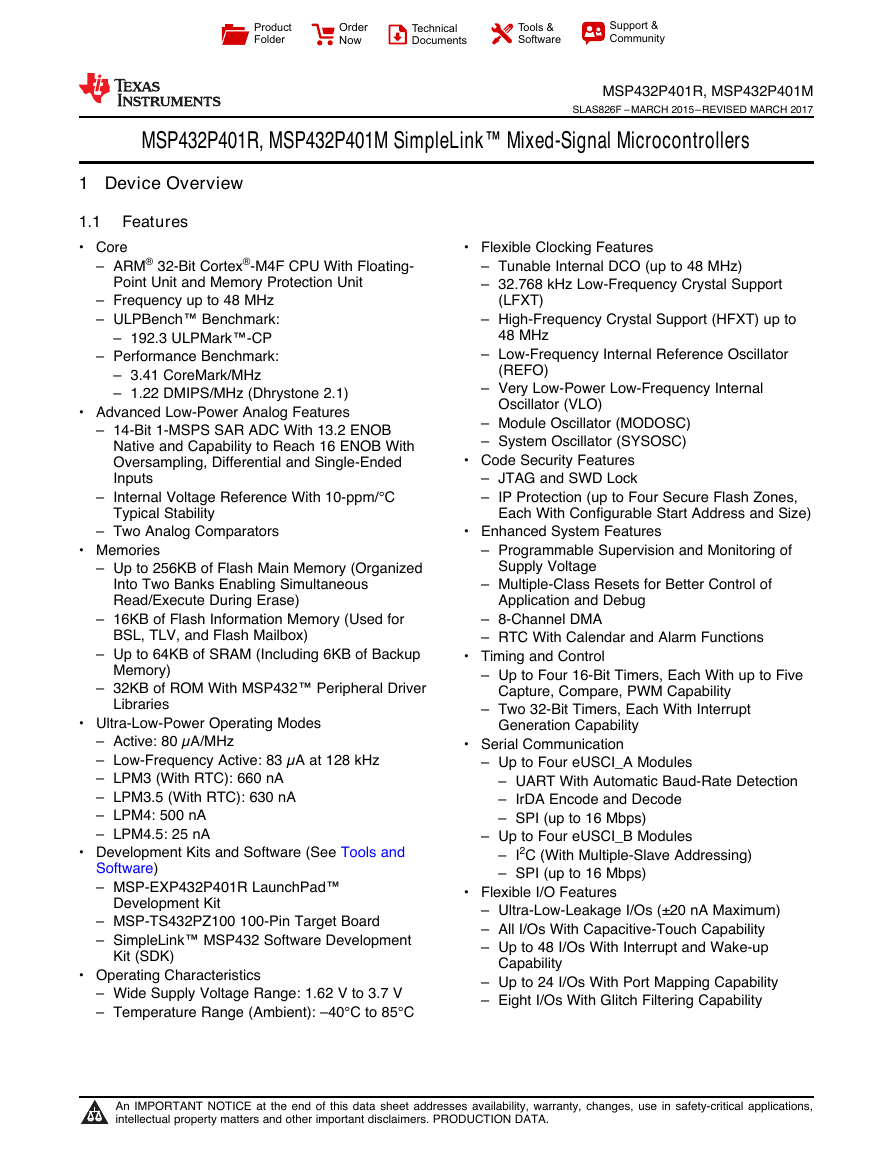
1 Device Overview
1.1 Features
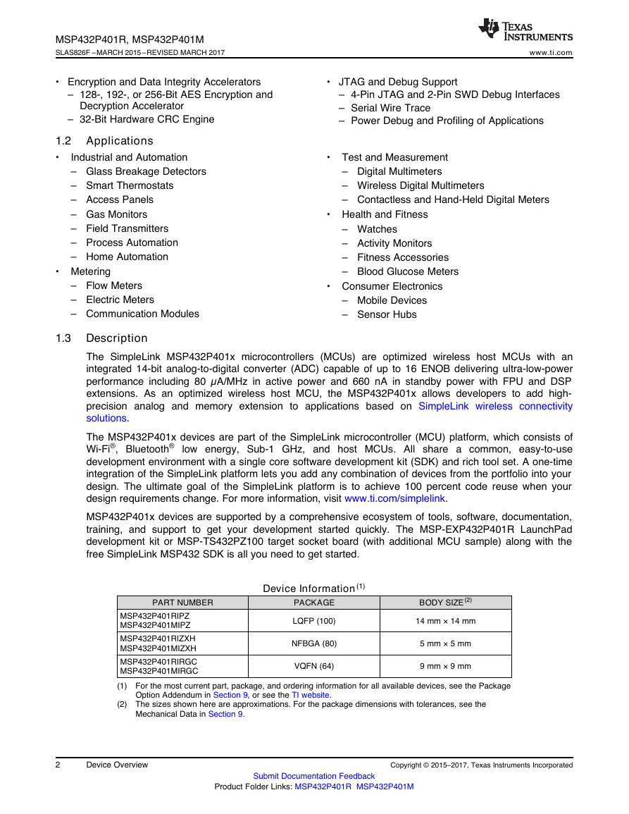
1.2 Applications
1.3 Description
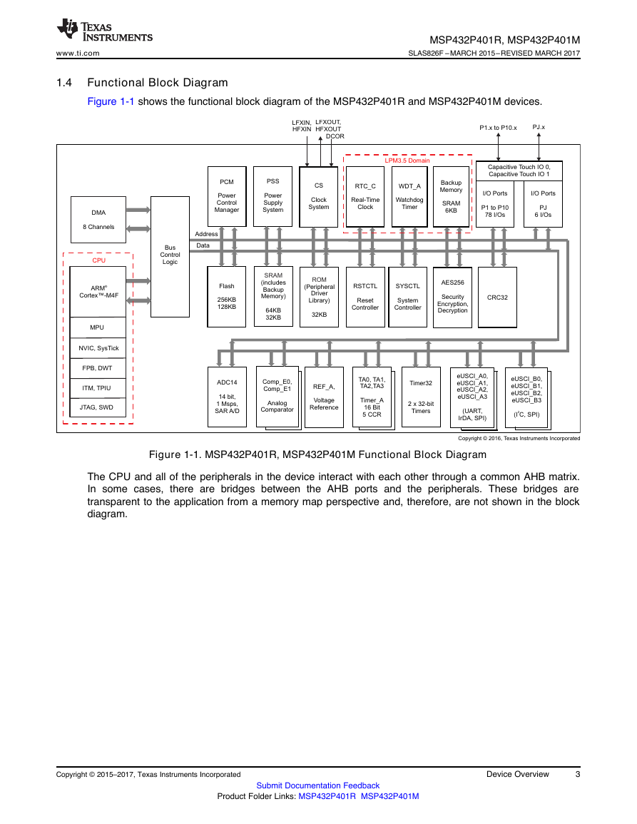
1.4 Functional Block Diagram
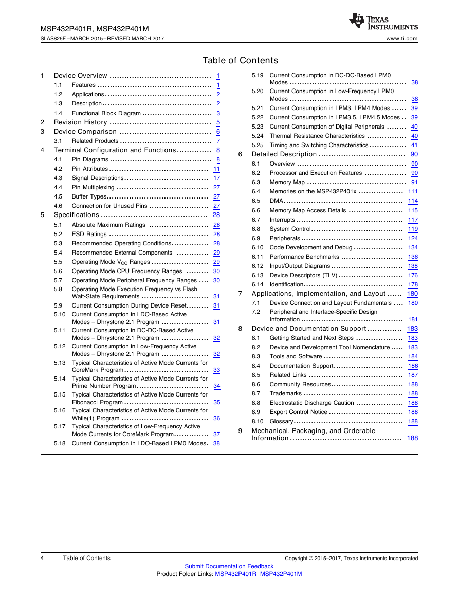
Table of Contents
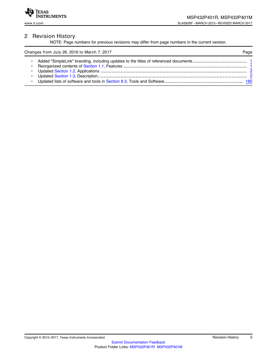
2 Revision History
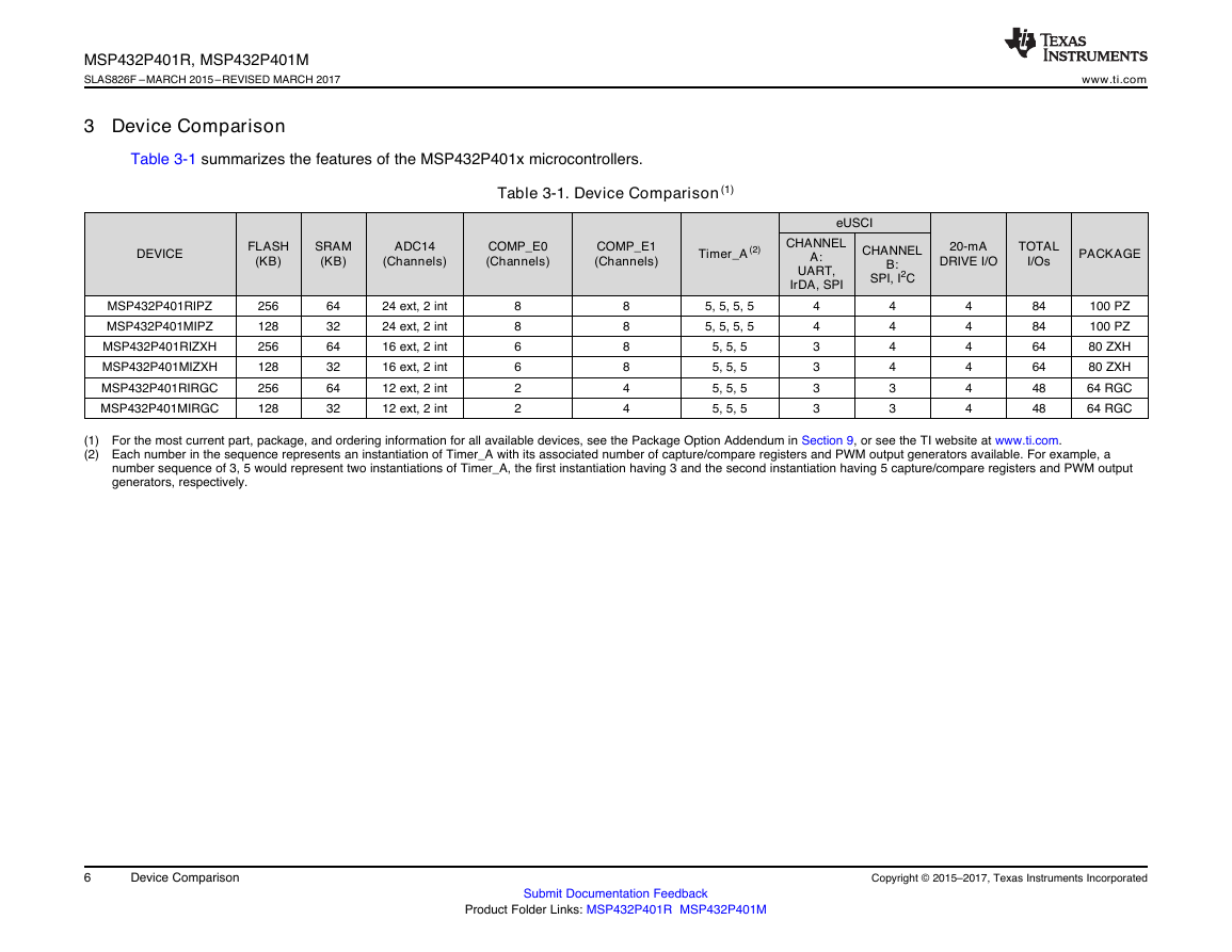
3 Device Comparison
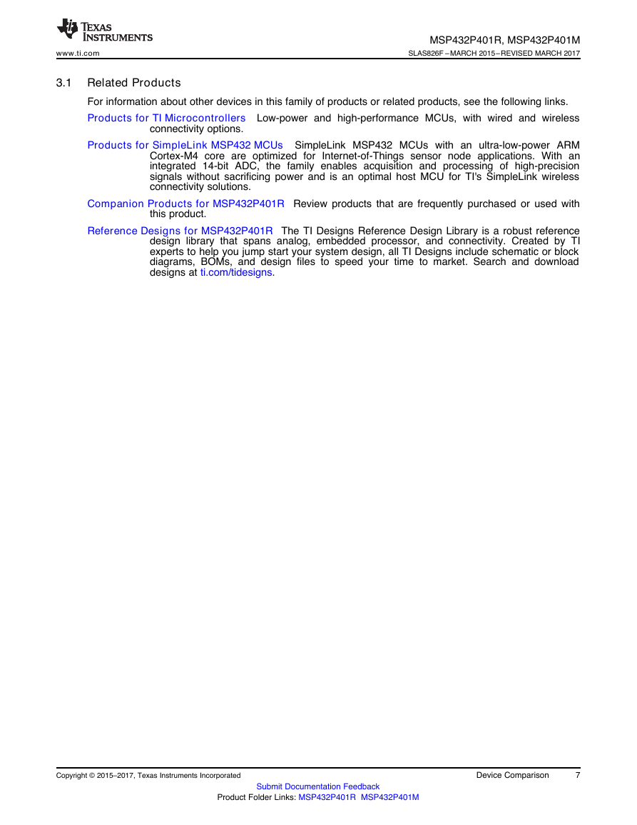
3.1 Related Products
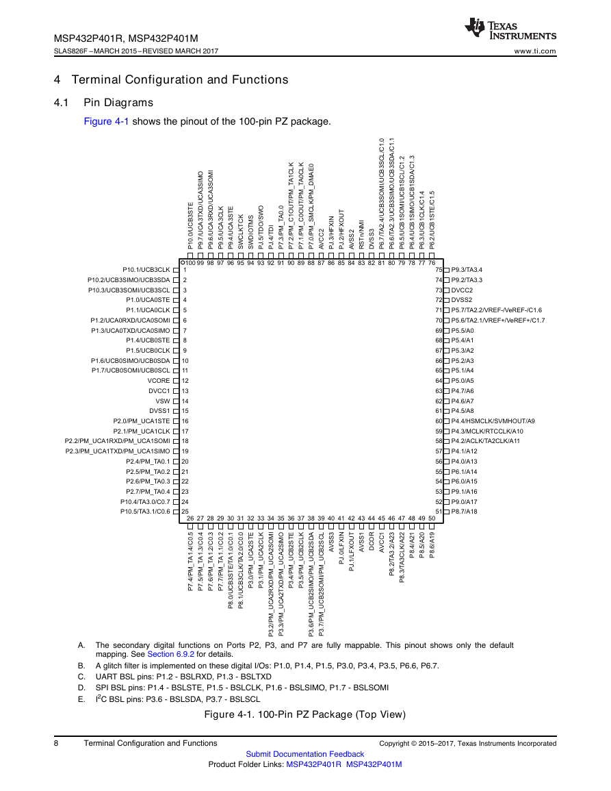
4 Terminal Configuration and Functions
4.1 Pin Diagrams
4.2 Pin Attributes
4.3 Signal Descriptions
4.4 Pin Multiplexing
4.5 Buffer Types
4.6 Connection for Unused Pins
5 Specifications
5.1 Absolute Maximum Ratings
5.2 ESD Ratings
5.3 Recommended Operating Conditions
5.4 Recommended External Components
5.5 Operating Mode VCC Ranges
5.6 Operating Mode CPU Frequency Ranges
5.7 Operating Mode Peripheral Frequency Ranges
5.8 Operating Mode Execution Frequency vs Flash Wait-State Requirements
5.9 Current Consumption During Device Reset
5.10 Current Consumption in LDO-Based Active Modes – Dhrystone 2.1 Program
5.11 Current Consumption in DC-DC-Based Active Modes – Dhrystone 2.1 Program
5.12 Current Consumption in Low-Frequency Active Modes – Dhrystone 2.1 Program
5.13 Typical Characteristics of Active Mode Currents for CoreMark Program
5.14 Typical Characteristics of Active Mode Currents for Prime Number Program
5.15 Typical Characteristics of Active Mode Currents for Fibonacci Program
5.16 Typical Characteristics of Active Mode Currents for While(1) Program
5.17 Typical Characteristics of Low-Frequency Active Mode Currents for CoreMark Program
5.18 Current Consumption in LDO-Based LPM0 Modes
5.19 Current Consumption in DC-DC-Based LPM0 Modes
5.20 Current Consumption in Low-Frequency LPM0 Modes
5.21 Current Consumption in LPM3, LPM4 Modes
5.22 Current Consumption in LPM3.5, LPM4.5 Modes
5.23 Current Consumption of Digital Peripherals
5.24 Thermal Resistance Characteristics
5.25 Timing and Switching Characteristics
5.25.1 Reset Timing
5.25.2 Mode Transition Timing
5.25.3 Clock Specifications
5.25.4 Power Supply System
5.25.5 Digital I/Os
5.25.5.1 Typical Characteristics, Normal-Drive I/O Outputs at 3.0 V and 2.2 V
5.25.5.2 Typical Characteristics, High-Drive I/O Outputs at 3.0 V and 2.2 V
5.25.5.3 Typical Characteristics, Pin-Oscillator Frequency
5.25.6 14-Bit ADC
5.25.6.1 Typical Characteristics of ADC
5.25.7 REF_A
5.25.8 Comparator_E
5.25.9 eUSCI
5.25.10 Timers
5.25.11 Memories
5.25.12 Emulation and Debug
6 Detailed Description
6.1 Overview
6.2 Processor and Execution Features
6.2.1 Floating-Point Unit
6.2.2 Memory Protection Unit
6.2.3 Nested Vectored Interrupt Controller (NVIC)
6.2.4 SysTick
6.2.5 Debug and Trace Features
6.3 Memory Map
6.3.1 Code Zone Memory Map
6.3.1.1 Flash Memory Region
6.3.1.2 SRAM Region
6.3.1.3 ROM Region
6.3.2 SRAM Zone Memory Map
6.3.2.1 SRAM Region
6.3.2.2 SRAM Bit-Band Alias Region
6.3.3 Peripheral Zone Memory Map
6.3.3.1 Peripheral Region
6.3.3.2 Peripheral Bit Band Alias Region
6.3.4 Debug and Trace Peripheral Zone
6.4 Memories on the MSP432P401x
6.4.1 Flash Memory
6.4.1.1 Flash Main Memory (0x0000_0000 to 0x0003_FFFF)
6.4.1.2 Flash Information Memory (0x0020_0000 to 0x0020_3FFF)
6.4.1.3 Flash Operation
6.4.2 SRAM
6.4.2.1 SRAM Bank Enable Configuration
6.4.2.2 SRAM Bank Retention Configuration and Backup Memory
6.4.3 ROM
6.5 DMA
6.5.1 DMA Source Mapping
6.5.2 DMA Completion Interrupts
6.5.3 DMA Access Privileges
6.6 Memory Map Access Details
6.6.1 Master and Slave Access Priority Settings
6.6.2 Memory Map Access Response
6.7 Interrupts
6.7.1 NMI
6.7.2 Device-Level User Interrupts
6.8 System Control
6.8.1 Device Resets
6.8.1.1 Power On/Off Reset (POR)
6.8.1.2 Reboot Reset
6.8.1.3 Hard Reset
6.8.1.4 Soft Reset
6.8.2 Power Supply System (PSS)
6.8.2.1 VCCDET
6.8.2.2 Supply Supervisor and Monitor for High Side (SVSMH)
6.8.2.3 Core Voltage Regulator
6.8.3 Power Control Manager (PCM)
6.8.4 Clock System (CS)
6.8.4.1 LFXT
6.8.4.2 HFXT
6.8.4.3 DCO
6.8.4.4 Very Low-Power Low-Frequency Oscillator (VLO)
6.8.4.5 Low-Frequency Reference Oscillator (REFO)
6.8.4.6 Module Oscillator (MODOSC)
6.8.4.7 System Oscillator (SYSOSC)
6.8.4.8 Fail-Safe Mechanisms
6.8.5 System Controller (SYSCTL)
6.9 Peripherals
6.9.1 Digital I/O
6.9.1.1 Glitch Filtering on Digital I/Os
6.9.2 Port Mapping Controller (PMAPCTL)
6.9.2.1 Port Mapping Definitions
6.9.3 Timer_A
6.9.3.1 Timer_A Signal Connection Tables
6.9.4 Timer32
6.9.5 Enhanced Universal Serial Communication Interface (eUSCI)
6.9.6 Real-Time Clock (RTC_C)
6.9.7 Watchdog Timer (WDT_A)
6.9.8 ADC14
6.9.9 Comparator_E (COMP_E)
6.9.10 Shared Reference (REF_A)
6.9.11 CRC32
6.9.12 AES256 Accelerator
6.9.13 True Random Seed
6.10 Code Development and Debug
6.10.1 JTAG and SWD Based Development, Debug, and Trace
6.10.2 Peripheral Halt Control
6.10.3 Bootloader (BSL)
6.10.4 Device Security
6.11 Performance Benchmarks
6.11.1 ULPBench Performance: 192.3 ULPMark-CP
6.11.2 CoreMark/MHz Performance: 3.41
6.11.3 DMIPS/MHz (Dhrystone 2.1) Performance: 1.22
6.12 Input/Output Diagrams
6.12.1 Port P1 (P1.0 to P1.7) Input/Output With Schmitt Trigger
6.12.2 Port P2 (P2.0 to P2.3) Input/Output With Schmitt Trigger
6.12.3 Port P3 (P3.0 to P3.7) Input/Output With Schmitt Trigger
6.12.4 Port P9 (P9.4 to P9.7) Input/Output With Schmitt Trigger
6.12.5 Port P10 (P10.0 to P10.3) Input/Output With Schmitt Trigger
6.12.6 Port P2 (P2.4 to P2.7) Input/Output With Schmitt Trigger
6.12.7 Port P7 (P7.0 to P7.3) Input/Output With Schmitt Trigger
6.12.8 Port P9 (P9.2 and P9.3) Input/Output With Schmitt Trigger
6.12.9 Port P4 (P4.0 to P4.7) Input/Output With Schmitt Trigger
6.12.10 Port P5 (P5.0 to P5.5) Input/Output With Schmitt Trigger
6.12.11 Port P6 (P6.0 and P6.1) Input/Output With Schmitt Trigger
6.12.12 Port P8 (P8.2 to P8.7) Input/Output With Schmitt Trigger
6.12.13 Port P9 (P9.0 and P9.1) Input/Output With Schmitt Trigger
6.12.14 Port P5 (P5.6 and P5.7) Input/Output With Schmitt Trigger
6.12.15 Port P6 (P6.2 to P6.5) Input/Output With Schmitt Trigger
6.12.16 Port P6 (P6.6 and P6.7) Input/Output With Schmitt Trigger
6.12.17 Port P8 (P8.0 and P8.1) Input/Output With Schmitt Trigger
6.12.18 Port P10 (P10.4 and P10.5) Input/Output With Schmitt Trigger
6.12.19 Port P7 (P7.4 to P7.7) Input/Output With Schmitt Trigger
6.12.20 Port PJ (PJ.0 and PJ.1) Input/Output With Schmitt Trigger
6.12.21 Port PJ (PJ.2 and PJ.3) Input/Output With Schmitt Trigger
6.12.22 Port PJ (PJ.4 and PJ.5) Input/Output With Schmitt Trigger
6.12.23 Ports SWCLKTCK and SWDIOTMS With Schmitt Trigger
6.13 Device Descriptors (TLV)
6.14 Identification
6.14.1 Revision Identification
6.14.2 Device Identification
6.14.3 ARM Cortex-M4F ROM Table Based Part Number
7 Applications, Implementation, and Layout
7.1 Device Connection and Layout Fundamentals
7.1.1 Power Supply Decoupling and Bulk Capacitors
7.1.2 External Oscillator
7.1.3 General Layout Recommendations
7.1.4 Do's and Don'ts
7.2 Peripheral and Interface-Specific Design Information
7.2.1 ADC14 Peripheral
7.2.1.1 Partial Schematic
7.2.1.2 Design Requirements
7.2.1.3 Layout Guidelines
8 Device and Documentation Support
8.1 Getting Started and Next Steps
8.2 Device and Development Tool Nomenclature
8.3 Tools and Software
8.4 Documentation Support
8.5 Related Links
8.6 Community Resources
8.7 Trademarks
8.8 Electrostatic Discharge Caution
8.9 Export Control Notice
8.10 Glossary
9 Mechanical, Packaging, and Orderable Information
Important Notice


 2023年江西萍乡中考道德与法治真题及答案.doc
 2012年重庆南川中考生物真题及答案.doc
 2013年江西师范大学地理学综合及文艺理论基础考研真题.doc
 2020年四川甘孜小升初语文真题及答案I卷.doc
 2020年注册岩土工程师专业基础考试真题及答案.doc
 2023-2024学年福建省厦门市九年级上学期数学月考试题及答案.doc
 2021-2022学年辽宁省沈阳市大东区九年级上学期语文期末试题及答案.doc
 2022-2023学年北京东城区初三第一学期物理期末试卷及答案.doc
 2018上半年江西教师资格初中地理学科知识与教学能力真题及答案.doc
 2012年河北国家公务员申论考试真题及答案-省级.doc
 2020-2021学年江苏省扬州市江都区邵樊片九年级上学期数学第一次质量检测试题及答案.doc
 2022下半年黑龙江教师资格证中学综合素质真题及答案.doc