Handout #2: EE314 Winter 2007
STANFORD UNIVERSITY
Department of Electrical Engineering
Problem Set 1
Due: Wednesday, 17 January 2007
________________________________________________________________________
Reading: Chapters 3 and 4 [Chapter 4 is not necessary for this problem set, but we’ll
assume that you’ve read it before next lecture.] It is a lot of work to read and understand
every word, so don’t. Instead, read with the primary aim of getting familiar with what
information is located where, and what the basic underlying concepts are.
This problem set is intended to be relatively short, given the timing of holidays, etc.
Problem 1: Chapter 3, Problem 1.
Problem 2: Chapter 3, Problem 4.
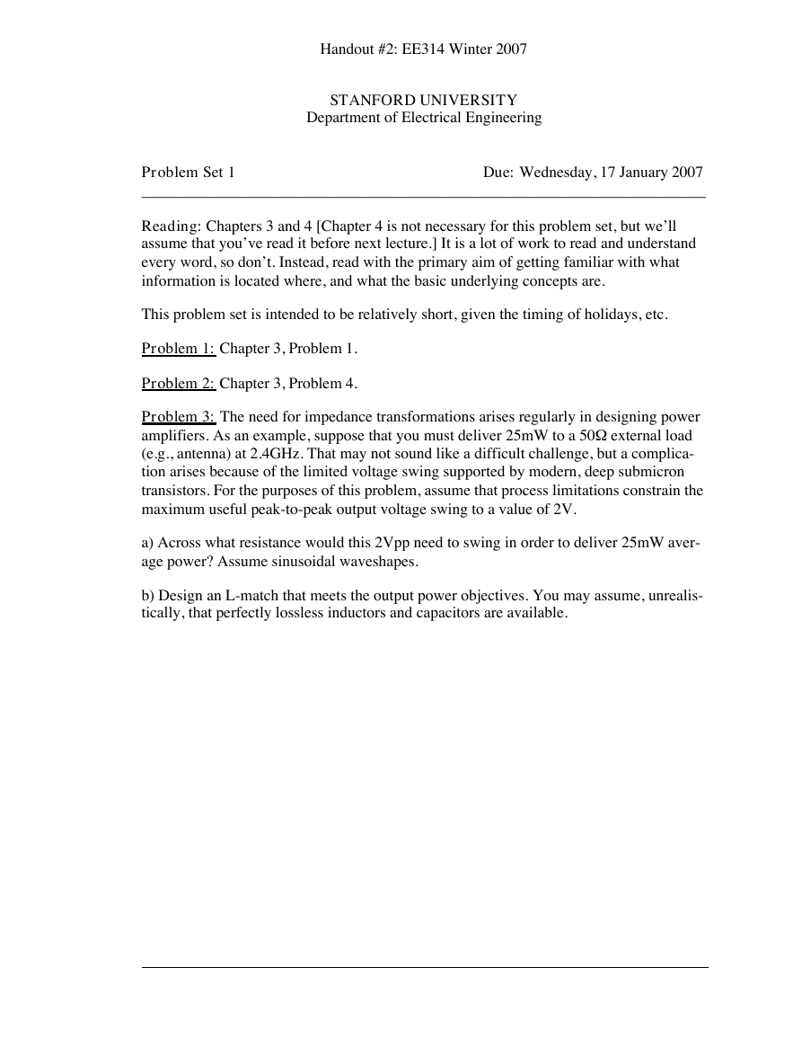
Problem 3: The need for impedance transformations arises regularly in designing power
amplifiers. As an example, suppose that you must deliver 25mW to a 50W
external load
(e.g., antenna) at 2.4GHz. That may not sound like a difficult challenge, but a complica-
tion arises because of the limited voltage swing supported by modern, deep submicron
transistors. For the purposes of this problem, assume that process limitations constrain the
maximum useful peak-to-peak output voltage swing to a value of 2V.
a) Across what resistance would this 2Vpp need to swing in order to deliver 25mW aver-
age power? Assume sinusoidal waveshapes.
b) Design an L-match that meets the output power objectives. You may assume, unrealis-
tically, that perfectly lossless inductors and capacitors are available.
�
Handout #4: EE314 Winter 2007
STANFORD UNIVERSITY
Department of Electrical Engineering
Problem Set 2
Due: Wednesday, 24 January 2007
________________________________________________________________________
Reading: Chapter 5.4.5 (read/skim the rest of the chapter if you need a refresher on MOS
physics); Chapter 6. Note: Those of you taking Quals may turn this in on January 31st,
along with Problem Set 3, which will be due then as well.
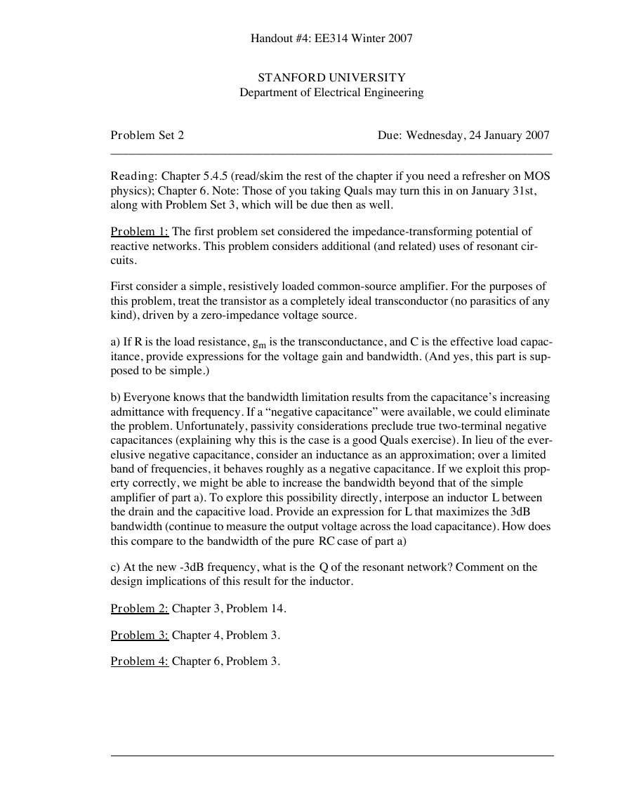
Problem 1: The first problem set considered the impedance-transforming potential of
reactive networks. This problem considers additional (and related) uses of resonant cir-
cuits.
First consider a simple, resistively loaded common-source amplifier. For the purposes of
this problem, treat the transistor as a completely ideal transconductor (no parasitics of any
kind), driven by a zero-impedance voltage source.
a) If R is the load resistance, gm is the transconductance, and C is the effective load capac-
itance, provide expressions for the voltage gain and bandwidth. (And yes, this part is sup-
posed to be simple.)
b) Everyone knows that the bandwidth limitation results from the capacitance’s increasing
admittance with frequency. If a “negative capacitance” were available, we could eliminate
the problem. Unfortunately, passivity considerations preclude true two-terminal negative
capacitances (explaining why this is the case is a good Quals exercise). In lieu of the ever-
elusive negative capacitance, consider an inductance as an approximation; over a limited
band of frequencies, it behaves roughly as a negative capacitance. If we exploit this prop-
erty correctly, we might be able to increase the bandwidth beyond that of the simple
amplifier of part a). To explore this possibility directly, interpose an inductor L between
the drain and the capacitive load. Provide an expression for L that maximizes the 3dB
bandwidth (continue to measure the output voltage across the load capacitance). How does
this compare to the bandwidth of the pure RC case of part a)
c) At the new -3dB frequency, what is the Q of the resonant network? Comment on the
design implications of this result for the inductor.
Problem 2: Chapter 3, Problem 14.
Problem 3: Chapter 4, Problem 3.
Problem 4: Chapter 6, Problem 3.
�
Handout #5: EE314 Winter 2007
STANFORD UNIVERSITY
Department of Electrical Engineering
Problem Set 3
Due: Wednesday, 31 January 2007
________________________________________________________________________
Reading: Chapter 9.
Problem 1: Chapter 9, Problem 1. a) Derive analytical expressions for the gain and phase
as a function of frequency, with m as a parameter. Then arbitrarily set C = 1pF, R = 100W
.
Vary m by varying L appropriately, and provide Spice simulation results for the specified
range of m. You should use these simulations to verify that your analytical expressions are
correct.
b) LTspice has a handy feature that also plots the delay as a function of frequency. Use
this feature to plot delay behavior for the various values of m. Use these plots to verify the
book’s derivation of the “maximally flat delay” condition for the shunt-peaked amplifier.
Problem 2: Chapter 9, Problem 9.
Problem 3: Footnote 10 on page 300 alludes to an alternate derivation of the optimum
gain per stage for an infinite cascade of identical amplifiers. Carry out this derivation for-
mally. You may use the basic approach of section 9.7.2 as a guide (but you are by no
means required to do so). This open-circuit-time constant-based derivation is perhaps
more commonly encountered, but you see that it yields a different (somewhat wrong)
answer.
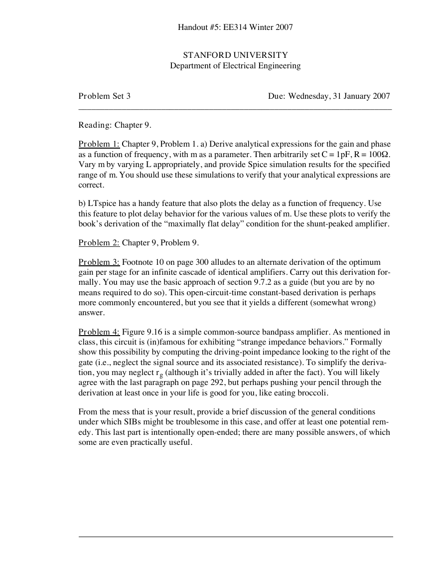
Problem 4: Figure 9.16 is a simple common-source bandpass amplifier. As mentioned in
class, this circuit is (in)famous for exhibiting “strange impedance behaviors.” Formally
show this possibility by computing the driving-point impedance looking to the right of the
gate (i.e., neglect the signal source and its associated resistance). To simplify the deriva-
tion, you may neglect rg (although it’s trivially added in after the fact). You will likely
agree with the last paragraph on page 292, but perhaps pushing your pencil through the
derivation at least once in your life is good for you, like eating broccoli.
From the mess that is your result, provide a brief discussion of the general conditions
under which SIBs might be troublesome in this case, and offer at least one potential rem-
edy. This last part is intentionally open-ended; there are many possible answers, of which
some are even practically useful.
�
Handout #9: EE314 Winter 2007
STANFORD UNIVERSITY
Department of Electrical Engineering
Problem Set 4
Due: Wednesday, 7 February 2007
________________________________________________________________________
Reading: Chapter 12: section 12.6 through to the end.
Problem 1: Chapter 12, problem 9.
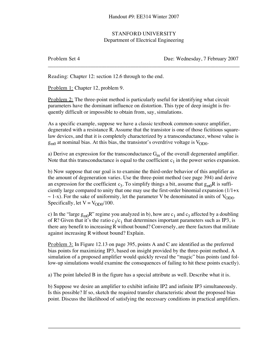
Problem 2: The three-point method is particularly useful for identifying what circuit
parameters have the dominant influence on distortion. This type of deep insight is fre-
quently difficult or impossible to obtain from, say, simulations.
As a specific example, suppose we have a classic textbook common-source amplifier,
degnerated with a resistance R. Assume that the transistor is one of those fictitious square-
law devices, and that it is completely characterized by a transconductance, whose value is
gm0 at nominal bias. At this bias, the transistor’s overdrive voltage is VOD0.
a) Derive an expression for the transconductance Gm of the overall degenerated amplifier.
Note that this transconductance is equal to the coefficient c1 in the power series expansion.
b) Now suppose that our goal is to examine the third-order behavior of this amplifier as
the amount of degeneration varies. Use the three-point method (see page 394) and derive
an expression for the coefficient c3. To simplify things a bit, assume that gm0R is suffi-
ciently large compared to unity that one may use the first-order binomial expansion (1/1+x
~ 1-x). For the sake of uniformity, let the parameter V be denominated in units of VOD0.
Specifically, let V = VOD0/100.
c) In the “large gm0R” regime you analyzed in b), how are c1 and c3 affected by a doubling
of R? Given that it’s the ratio c3/c1 that determines important parameters such as IP3, is
there any benefit to increasing R without bound? Conversely, are there factors that militate
against increasing R without bound? Explain.
Problem 3: In Figure 12.13 on page 395, points A and C are identified as the preferred
bias points for maximizing IP3, based on insight provided by the three-point method. A
simulation of a proposed amplifier would quickly reveal the “magic” bias points (and fol-
low-up simulations would examine the consequences of failing to hit these points exactly).
a) The point labeled B in the figure has a special attribute as well. Describe what it is.
b) Suppose we desire an amplifier to exhibit infinite IP2 and infinite IP3 simultaneously.
Is this possible? If so, sketch the required transfer characteristic about the proposed bias
point. Discuss the likelihood of satisfying the necessary conditions in practical amplifiers.
�
Handout #10: EE314 Winter 2007
STANFORD UNIVERSITY
Department of Electrical Engineering
Problem Set 4
Due: Wednesday, 14 February 2007
________________________________________________________________________
(This problem set is effectively the first part of the midterm design problem.)
Reading: LTspice tutorial/documentation, as needed.
Problem 1: The purpose of this exercise is to develop a familiarity with the characteristics
of the 180nm-technology you’ll be using for the midterm design project. Use the SPICE
models provided (see the class website, and extract only the part of the file that actually
contains the models), and plot ID vs. VDS with VGS as a parameter for a 100m m-wide,
minimum-length device. Vary VDS and VGS from 0 to 1.8V, and step VGS in increments
of 100mV.
a) Standard textbook MOSFETs behave in ways that differ from real ones. To highlight
just one of these differences, note the behavior of the output resistance as a function of
operating point. Standard MOS theory has the output resistance varying inversely with
bias current, but a better fit for many modern devices (like the ones you’ll be using) is an
inverse square-root dependence. Specifically, you will find that, over a wide portion of the
saturation region, the output resistance will be roughly proportional to the square-root of
the drain current. Using any method of your choice, provide the corresponding proportion-
ality constant. Note the dimensions of this constant.
b) Another difference is the short-channel effect on VDsat. Overlay a hand sketch of the
long-channel VDsat on your I-V plot. Then, using your eyeball, sketch a more relevant
VDsat curve on the same plot. Note how, in this case, short-channel effects are actually
quite helpful.
c) Yet another difference is found in the behavior of gm. Classical textbook theory has gm
increasing with bias current, but your transistors will not behave this way. For this process
technology, what is the peak transconductance over the bias range given? Again, it is per-
fectly fine to use graphical techniques, as all we’re seeking is to build familiarity; an
approximate value is more than acceptable. But if you wish, feel free to construct a test
circuit and discover the peak value formally.
Problem 2: For the same transistor as in Problem 1, explore how to evaluate nonlinearity
with a two-tone test. The idea is to develop a facility with FFTs (particularly how to avoid
incorrect results). For the sake of uniformity in answers, assume a common-source config-
uration. Bias the gate with an ideal 0.5V source, and tie the drain to an ideal 1V source.
Let the two tones be at 2.4GHz and 2.45GHz, and superpose them on the bias source ide-
ally (i.e., use no added impedances of any kind). Plot the drain current spectrum when
each of the two tones has an amplitude of 25mV.
�
Handout #10: EE314 Winter 2007
Problem 3: In addition to the fundamental nonlinearity of a MOSFET’s transconduc-
tance, another important source of nonlinearity in MOS PAs is the nonlinear gate-source
capacitance. A power amplifier typically drives the gate both above and below threshold.
Recall that the small-signal capacitance in these two regimes is quite different. The signal-
dependent variation in capacitance generates additional distortion which can actually
dominate in certain practical situations.
Connect the transistor of Problem 1 as a capacitor (tie drain and source together, and
ground them). First drive the gate with a single sinusoidal source at 2.5GHz. Let its ampli-
tude be 250mV. Examine the harmonic distortion of the gate current as you vary the gate
bias (through the addition of a suitable ideal DC source) from 0 to 1V in 250mV steps.
�
EE314: CMOS RF Design
Prof. Thomas H. Lee
Stanford University
Winter 2007
Homework 1 Solution
Last updated January 19, 2007
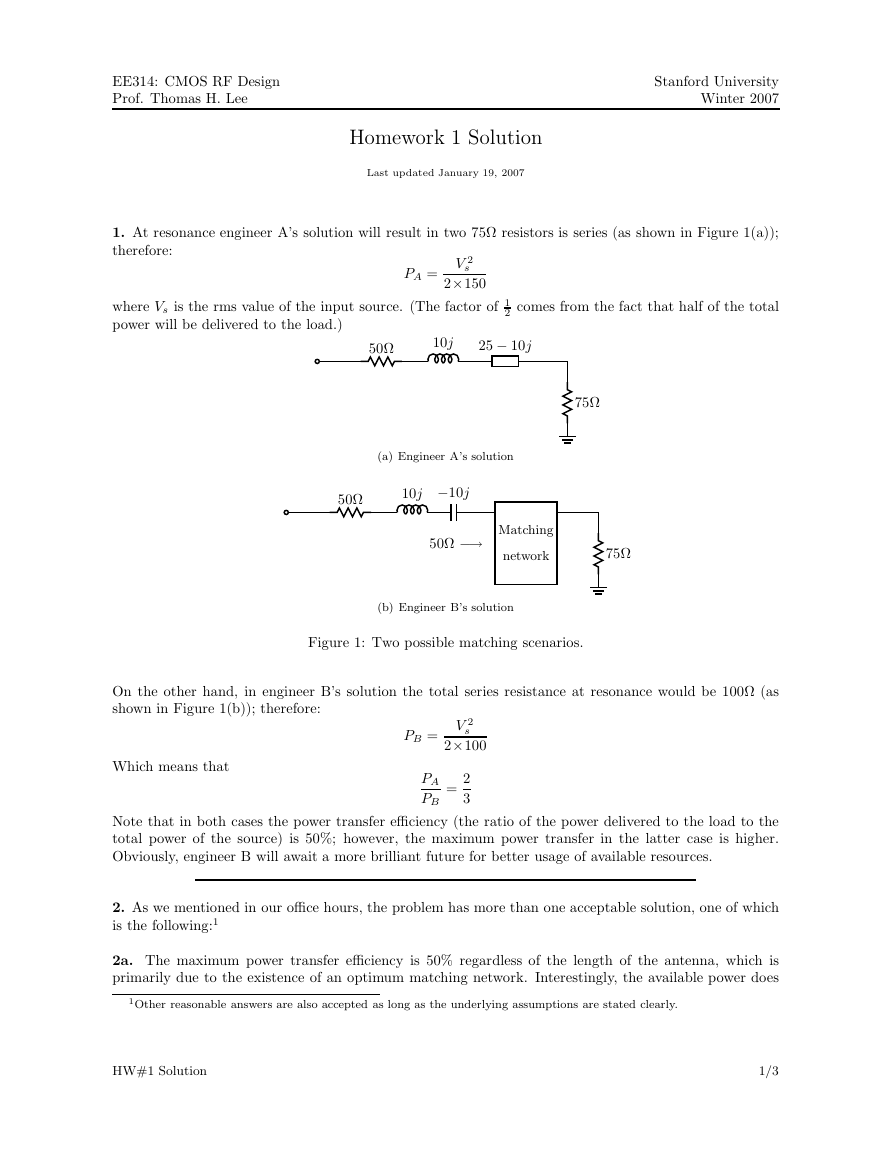
1. At resonance engineer A’s solution will result in two 75Ω resistors is series (as shown in Figure 1(a));
therefore:
PA =
V 2
s
2×150
where Vs is the rms value of the input source. (The factor of 1
power will be delivered to the load.)
2 comes from the fact that half of the total
50Ω
10j
25 − 10j
75Ω
(a) Engineer A’s solution
50Ω
10j −10j
50Ω −→
Matching
network
75Ω
(b) Engineer B’s solution
Figure 1: Two possible matching scenarios.
On the other hand, in engineer B’s solution the total series resistance at resonance would be 100Ω (as
shown in Figure 1(b)); therefore:
Which means that
PB =
V 2
s
2×100
PA
PB
=
2
3
Note that in both cases the power transfer efficiency (the ratio of the power delivered to the load to the
total power of the source) is 50%; however, the maximum power transfer in the latter case is higher.
Obviously, engineer B will await a more brilliant future for better usage of available resources.
2. As we mentioned in our office hours, the problem has more than one acceptable solution, one of which
is the following:1
2a. The maximum power transfer efficiency is 50% regardless of the length of the antenna, which is
primarily due to the existence of an optimum matching network. Interestingly, the available power does
1Other reasonable answers are also accepted as long as the underlying assumptions are stated clearly.
HW#1 Solution
1/3
�
EE314: CMOS RF Design
Prof. Thomas H. Lee
Stanford University
Winter 2007
not depend on the antenna length either; because the voltage increases linearly with l while the impedance
increases quadratically thereby keeping power constant:
PL =
PSys =
V 2
×Rrad
s
2R2
rad
=
V 2
s
4Rrad
=
E2λ2
1580
=
E2λ2
790
V 2
s
Rtot
=⇒
V 2
s
=
2Rrad
1
2
=
PL
PSys
2b. In this case again the maximum power transfer efficiency is 50% (assuming that the matching network
is redesigned properly); however, you would always want to minimize the effect of resistive losses in the
antenna, in which case you may want to increase the length of the antenna to increase the ratio of Rrad
.
Rd
From another perspective, similar to the previous problem, having more source resistance will limit the
maximum available power of a given source.
PL =
PSys =
V 2
s ×(Rrad + Rd)
(2Rrad + 2Rd)2 =
V 2
s
Rtot
2Rrad + 2Rd
V 2
s
=
V 2
s
4(Rrad + Rd)
=⇒
PL
PSys
=
1
2
Here we have assumed that the matching network is changed to match Rrad + Rd; however, if you assume
that the matching network is the same as Part a you will find that:
PTE =
RL
RL + Rrad + Rd
where RL is the load impedance looking into the matching network. This equation confirms that to achieve
maximum power transfer efficieny one should minimize Rd.
Note that the main purpose of this problem and the previous one is to show you that maximum power
transfer and maximum power transfer efficiency are not the same.
If Wikipedia’s entry on maximum
power transfer is to be believed this is a subtly that has confused minds as great as Joule’s:
“The theorem was originally misunderstood (notably by Joule) to imply that a system consisting of an
electric motor driven by a battery could not be more than 50% efficient since, when the impedances were
matched, the power lost as heat in the battery would always be equal to the power delivered to the motor.
In 1880 this assumption was shown to be false by either Edison or his colleague Francis Robbins Upton,
who realized that maximum efficiency was not the same as maximum power transfer.”
3a.
P =
v2
2R
=
1
2×R
= 25mW
−→ R =
1
0.05
= 20Ω
3b. There are two possible solutions as shown in Figure 2:
HW#1 Solution
2/3
�


 2023年江西萍乡中考道德与法治真题及答案.doc
 2012年重庆南川中考生物真题及答案.doc
 2013年江西师范大学地理学综合及文艺理论基础考研真题.doc
 2020年四川甘孜小升初语文真题及答案I卷.doc
 2020年注册岩土工程师专业基础考试真题及答案.doc
 2023-2024学年福建省厦门市九年级上学期数学月考试题及答案.doc
 2021-2022学年辽宁省沈阳市大东区九年级上学期语文期末试题及答案.doc
 2022-2023学年北京东城区初三第一学期物理期末试卷及答案.doc
 2018上半年江西教师资格初中地理学科知识与教学能力真题及答案.doc
 2012年河北国家公务员申论考试真题及答案-省级.doc
 2020-2021学年江苏省扬州市江都区邵樊片九年级上学期数学第一次质量检测试题及答案.doc
 2022下半年黑龙江教师资格证中学综合素质真题及答案.doc