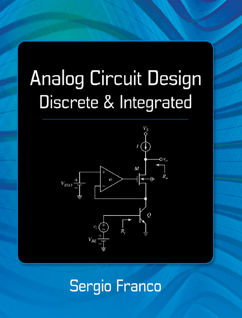
Front Cover
Title Page
Copyright Page
Dedication Page
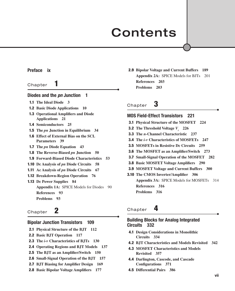
CONTENTS (with direct page links)
Preface
A word of advice to the student
1. Diodes and the pn Junction
1.1 The Ideal Diode
1.2 Basic Diode Applications
1.3 Operational Amplifiers and Diode Applications
1.4 Semiconductors
1.5 The pn Junction in Equilibrium
1.6 Effect of External Bias on the SCL Parameters
1.7 The pn Diode Equation
1.8 The Reverse-Biased pn Junction
1.9 Forward-Biased Diode Characteristics
1.10 Dc Analysis of pn Diode Circuits
1.11 Ac Analysis of pn Diode Circuits
1.12 Breakdown-Region Operation
1.13 Dc Power Supplies
Appendix 1A: SPICE Models for Diodes
References
Problems
2. Bipolar Junction Transistors
2.1 Physical Structure of the BJT
2.2 Basic BJT Operation
2.3 The i-v Characteristics of BJTs
2.4 Operating Regions and BJT Models
2.5 The BJT as an Amplifier/Switch
2.6 Small-Signal Operation of the BJT
2.7 BJT Biasing for Amplifier Design
2.8 Basic Bipolar Voltage Amplifiers
2.9 Bipolar Voltage and Current Buffers
Appendix 2A: SPICE Models for BJTs
References
Problems
3. MOS Field-Effect Transistors
3.1 Physical Structure of the MOSFET
3.2 The Threshold Voltage V[sub(t)]
3.3 The n-Channel Characteristic
3.4 The i-v Characteristics of MOSFETs
3.5 MOSFETs in Resistive Dc Circuits
3.6 The MOSFET as an Amplifier/Switch
3.7 Small-Signal Operation of the MOSFET
3.8 Basic MOSFET Voltage Amplifiers
3.9 MOSFET Voltage and Current Buffers
3.10 The CMOS Inverter/Amplifier
Appendix 3A: SPICE Models for MOSFETs
References
Problems
4. Building Blocks for Analog Integrated Circuits
4.1 Design Considerations in Monolithic Circuits
4.2 BJT Characteristics and Models Revisited
4.3 MOSFET Characteristics and Models Revisited
4.4 Darlington, Cascode, and Cascade Configurations
4.5 Differential Pairs
4.6 Common-Mode Rejection Ratio in Differential Pairs
4.7 Input Offset Voltage/Current in Differential Pairs
4.8 Current Mirrors
4.9 Differential Pairs with Active Loads
4.10 Bipolar Output Stages
4.11 CMOS Output Stages
Appendix 4A: Editing SPICE Netlists
References
Problems
5. Analog Integrated Circuits
5.1 The μA741 Operational Amplifier
5.2 The Two-Stage CMOS Operational Amplifier
5.3 The Folded-Cascode CMOS Operational Amplifier
5.4 Voltage Comparators
5.5 Current and Voltage References
5.6 Current-Mode Integrated Circuits
5.7 Fully Differential Operational Amplifiers
5.8 Switched-Capacitor Circuits
Appendix 5A: SPICE Macro-Models
References
Problems
6. Frequency and Time Responses
6.1 High-Frequency BJT Model
6.2 High-Frequency MOSFET Model
6.3 Frequency Response of CE/CS Amplifiers
6.4 Frequency Response of Differential Amplifiers
6.5 Bipolar Voltage and Current Buffers
6.6 MOS Voltage and Current Buffers
6.7 Open-Circuit Time-Constant (OCTC) Analysis
6.8 Frequency Response of Cascode Amplifiers
6.9 Frequency and Transient Responses of Op Amps
6.10 Diode Switching Transients
6.11 BJT Switching Transients
6.12 Transient Response of CMOS Gates and Voltage Comparators
Appendix 6A: Transfer Functions and Bode Plots
References
Problems
7. Feedback, Stability, and Noise
7.1 Negative-Feedback Basics
7.2 Effect of Feedback on Distortion, Noise, and Bandwidth
7.3 Feedback Topologies and Closed-Loop I/O Resistances
7.4 Practical Configurations and the Effect of Loading
7.5 Return Ratio Analysis
7.6 Blackman's Impedance Formula and Injection Methods
7.7 Stability in Negative-Feedback Circuits
7.8 Dominant-Pole Compensation
7.9 Frequency Compensation of Monolithic Op Amps
7.10 Noise
References
Problems
INDEX
A-B
C
D
E-F
G
H-I
J
L
M
N
O
P
Q-R
S
T
U
V
W
Z




 2023年江西萍乡中考道德与法治真题及答案.doc
 2012年重庆南川中考生物真题及答案.doc
 2013年江西师范大学地理学综合及文艺理论基础考研真题.doc
 2020年四川甘孜小升初语文真题及答案I卷.doc
 2020年注册岩土工程师专业基础考试真题及答案.doc
 2023-2024学年福建省厦门市九年级上学期数学月考试题及答案.doc
 2021-2022学年辽宁省沈阳市大东区九年级上学期语文期末试题及答案.doc
 2022-2023学年北京东城区初三第一学期物理期末试卷及答案.doc
 2018上半年江西教师资格初中地理学科知识与教学能力真题及答案.doc
 2012年河北国家公务员申论考试真题及答案-省级.doc
 2020-2021学年江苏省扬州市江都区邵樊片九年级上学期数学第一次质量检测试题及答案.doc
 2022下半年黑龙江教师资格证中学综合素质真题及答案.doc