logo资料库

Imx53UG 飞思卡尔A8嵌入式资料.pdf

第1页 / 共235页
第2页 / 共235页
第3页 / 共235页
第4页 / 共235页
第5页 / 共235页
第6页 / 共235页
第7页 / 共235页
第8页 / 共235页
资料共235页,剩余部分请下载后查看
i.MX53 System Development User’s Guide
Contents
Figures
Tables
About This Guide
Audience
Organization
Essential Reference
Suggested Reading
General Information
Related Documentation
Conventions
Signal Conventions
Acronyms and Abbreviations
Part I Hardware Design and Bring-up
Chapter 1 Design Checklist
Table 1-1. Design Checklist
1.1 Boot Configuration Bus Isolation Resistors
Figure 1-1. Boot Configuration Bus Isolation Resistors
1.2 DDR Reference Circuit
Table 1-2. DDR Vref Resistor Sizing Guideline (continued)
1.3 Avoiding I2C Conflicts
Table 1-3. I2C Bus Example Spreadsheet
Table 1-4. I2C Port Usage Scenario
1.4 JTAG Signal Termination
Table 1-5. JTAG Interface Summary
Table 1-6. Additional JTAG Signals
Chapter 2 i.MX53 Layout Recommendations
2.1 Basic Design Recommendations
Figure 2-1. i.MX53 Ball-Grid Array
Figure 2-2. i.MX53 Package Information
2.1.1 Fanout
Figure 2-3. i.MX53 Fanouts
2.2 Stackup
Figure 2-4. Layer Stack
Figure 2-5. Stackup Requirements
2.3 DDR Connection Information
Figure 2-6. Connection Between i.MX53 and DDR2 and DDR3
Figure 2-7. Final Placement of Memories and Decoupling Capacitors
2.4 DDR2 and DDR3 Routing Rules
Table 2-1. DDR2/DDR3 Routing by the Same Length
Table 2-2. DDR2/DDR3 Routing by Byte Group
2.5 Routing Topologies
2.5.1 1 Gbyte Topologies
Figure 2-8. Topology for ADDR/CMD/CTRL Signals
Figure 2-9. Topology of Data Group, Point-to-Point Connection
Figure 2-10. Topology for Data Bus of Two Byte Groups by Memory
Figure 2-11. Clock Routing Topology
2.5.2 2 Gbyte Topologies
Figure 2-12. ADDR/CMD Signal Routing
Figure 2-13. CTRL Signal Topology
Figure 2-14. Data Bus Routing Topology
Figure 2-15. Clock Routing Topology
2.5.3 DDR2 Routing Examples
Figure 2-16. Top DDR2 Routing
Figure 2-17. Internal 1 DDR2 Routing
Figure 2-18. Power Plane 1 DDR2 Routing
Figure 2-19. Power Plane 2 DDR2 Routing
Figure 2-20. Internal 2 DDR2 Routing
Figure 2-21. Bottom DDR2 Routing
Table 2-3. Total Signal Etch (DDR2)
2.5.4 2-Gbyte Routing Examples
Figure 2-22. Top 8-DDR3 Routing
Figure 2-23. Internal 1 8-DDR3 Routing
Figure 2-24. Power Plane 1 8-DDR3 Routing
Figure 2-25. Power Plane 2 8-DDR3 Routing
Figure 2-26. Internal 2 8-DDR3 Routing
Figure 2-27. Bottom 8-DDR3 Routing
Table 2-4. Total Signal Etch (DDR3)
2.6 Power Recommendations
2.7 TV Encoder Recommendations
2.8 SATA Recommendations
2.9 LVDS Recommendations
Figure 2-28. Microstrip and Stripline Differential Pair Dimensions
Figure 2-29. Differential Pair Routing
2.10 Reference Resistors
2.11 ESD and Radiated Emissions Recommendations
Chapter 3 Understanding the IBIS Model
3.1 IBIS Structure and Content
3.2 Header Information
Table 3-1. Header Information
3.3 Component and Pin Information
Table 3-2. Component and Pin Information (continued)
3.4 Model Information
Figure 3-1. Model IV Keywords’ Structure
3.4.1 Ramp and Waveform Keywords
Table 3-3. Ramp and Waveform Keywords
Figure 3-2. Model Data Interpretation
3.5 Model Golden Waveforms
Figure 3-3. Generic Test Load Network
Table 3-4. Golden Waveform Keywords
3.6 Naming Conventions for Model Names and Usage in i.MX53 IBIS File
3.6.1 [Model Selector] ddr
3.6.2 [Model Selector] gpio
3.6.3 [Model Selector] lvio
3.6.4 [Model Selector] uhvio
3.6.5 List of Pins Not Modeled in the i.MX53 IBIS File
Table 3-5. Unmodeled Analog or Special Interface Pins
Table 3-6. Unmodeled Differential Signals
3.7 Quality Assurance for the IBIS Models
3.8 References
Chapter 4 Using the IOMUX Design Aid
4.1 Application Requirements
4.2 IOMUX Tool Walkthrough
4.2.1 Identifying Signal Conflicts with the Signal Selection Pane
Figure 4-1. Application Window after Expanding UARTs 2 and 3 of i.MX35 TO2.1
Figure 4-2. Hovering Mouse over a Signal to Show Other Signals Sharing that Ball/Pin
Figure 4-3. Hovering Mouse over a Signal in the Signals Tab
Figure 4-4. Expanding UART3_RTS to Show Potential Conflicts
Figure 4-5. Resolving Conflicts by Changing Ball Assignments
4.2.2 Adding Comments with the Signals Tab
Figure 4-6. Signal Tab with Comment Entry Menu
Figure 4-7. UART2_TXD_MUX with Note
Figure 4-8. File > Save Dialog Box, Showing the Three Formats for Saving Design Info
4.3 Toggling the Alternate View of the Signals Tab
Figure 4-9. Display of Other Signals Available on an Assigned Ball
4.3.1 Finding Assigned Signal Locations with the Ball Diagram Tab
Figure 4-10. Choosing the Ball Diagram Tab Displays the Device’s Ball Map
4.4 Using the Search Box to Find Specific Signals or Balls
Figure 4-11. Basic Substring Text Searching
4.5 IOMUX Features Guide
Figure 4-12. IOMux.exe Application Window Overview
4.5.1 Title Bar
4.5.2 Menus
4.5.2.1 File Menu
Figure 4-13. Detailed View of File Menu
4.5.2.2 Device Menu
Figure 4-14. Detailed View of the Device Menu
4.5.2.3 View Menu
Figure 4-15. Detailed View of the View Menu
4.5.2.4 Help Menu
Figure 4-16. Detailed View of the Help Menu
4.5.3 Search Box
4.5.4 Signal Selection Pane
4.5.5 Signal Assignments and Ball Map Pane
4.5.5.1 Signals Tab
4.5.5.2 Ball Diagram Tab
4.5.6 Status Bar
Chapter 5 Setting up Power Management
5.1 i.MX53 Internal LDOs
Figure 5-1. Internal LDOs
5.2 Interfacing the i.MX53 Processor with the DA9053
Figure 5-2. Power-up Sequence
Table 5-1. i.MX53 Voltage Rails and Associated DA9053 Regulator (continued) (continued)
5.2.1 Connecting Power and Communication Signals
Figure 5-3. Power Connections
Figure 5-4. Communication Signal Connections
Figure 5-5. Interface Power-up Sequence (DA9053)
5.3 Interfacing the i.MX53 Processor with LTC3589-1
Figure 5-6. Power-up Sequence
5.3.1 Using the I2C Interface
5.3.2 I2C Acknowledge
5.4 Interface Table
Table 5-2. i.MX53 Voltage Rails and Associated LTC3589-1 Regulator (continued)
5.5 Connecting Power and Communication Signals
Figure 5-7. Power Connections Block (LT3481)
Figure 5-8. Power Connections Block, cont. (LTC3589-1)
Figure 5-9. Communication Signals Connections Block (LTC3589-1)
Figure 5-10. Communication Signals Connections Block, cont. (TPS73201, LT3481)
5.5.1 Powering-up the Interface
Figure 5-11. Interface Power-Up Sequence (LTC3589-1)
5.6 Additional Device Information
5.6.1 DA9053
Figure 5-12. DA9053 Typical Application Block Diagram
Table 5-3. Generated Supply Domains (continued)
5.6.2 LTC3589-1
Figure 5-13. LTC3589-1 Typical Application Block Guide
Table 5-4. LTC3589-1 Supply Domains
Chapter 6 Interfacing DDR2 and DDR3 Memories with the i.MX53 Processor
6.1 i.MX53 SDRAM Controller Signals
Figure 6-1. Connection Between i.MX53 Processor and DDR2 and DDR3
6.2 i.MX53 Memory Interface
Figure 6-2. DDR2 Memory Connection
Figure 6-3. DDR3 Memory Connection
6.3 Configuring the DDR2 JTAG Script
6.4 Configuring the DDR3 JTAG Script
6.5 Configuring the i.MX53 Registers for the Initialization Script
6.5.1 Main Control Register
Figure 6-4. Main Control Register
6.5.2 Power Down Register
Figure 6-5. Power Down Register
6.5.3 Timing Configuration 0 Register
Figure 6-6. Timing Configuration 0 Register
6.5.4 Timing Configuration 1 Register
Figure 6-7. Timing Configuration 1 Register
6.5.5 Timing Configuration 2 Register
Figure 8. ESDCTL Timing Configuration Register 2(ESDCFG2)
Chapter 7 Avoiding Board Bring-Up Problems
7.1 Using a Voltage Report to Avoid Power Pitfalls
Table 7-1. Sample Voltage Report
7.2 Using a Current Monitor to Avoid Power Pitfalls
7.3 Checking for Clock Pitfalls
7.4 Avoiding Reset Pitfalls
7.5 Sample Board Bring-Up Checklist
Table 7-2. Board Bring-Up Checklist (continued)
Chapter 8 Using the Clock Connectivity Table
Table 8-1. Clock Roots
Chapter 9 Configuring JTAG Tools for Debugging
9.1 Accessing Debug with a JTAG Scan Chain (ARM tools)
Figure 9-1. Example of Adding a Device
Figure 9-2. Updating the CoreSight Base Address
Figure 9-3. i.MX/Cortex-A8 RVDS JTAG Scan Chain
9.2 Accessing Debug with a JTAG Scan Chain (other JTAG tools)
Part II Software Development
Chapter 10 Porting the On-Board-Diagnostic-Suite (OBDS) to a Custom Board
10.1 Supported Components
10.2 Customizing OBDS for Specific Hardware
10.2.1 UART (serial port) Test
10.2.2 DDR Test
10.2.3 Audio Test
10.2.4 IPU Display Test
10.2.5 I2C Test
10.2.6 SD/MMC Test
10.2.7 LED Test
10.2.8 Ethernet (FEC) Loopback Test
10.2.9 SPI-NOR Test
Chapter 11 Porting U-Boot from an i.MX53 Reference Board to an i.MX53 Custom Board
11.1 Obtaining the Source Code for the U-Boot
11.2 Preparing the Code
11.3 Customizing the i.MX53 Custom Board Code
11.3.1 Changing the DCD Table for i.MX53 DDR3 Initialization
11.3.2 Booting with the Modified U-Boot
11.3.3 Further Customization at System Boot
11.3.4 Customizing the Printed Board Name
Chapter 12 Porting the Android Kernel
12.1 Patching the Android Kernel
12.2 Configuring Android Release for Customized Platforms
12.2.1 Enabling and Disabling Default Resources
Figure 12-1. Linux Kernel Configuration Menu
12.2.2 Changing the Configuration File
12.2.3 Android's Memory Map
Figure 12-2. Android Memory Map (512 Mbyte System)
12.3 Initializing Android
12.4 Modifying the init.rc Partition Locations
12.5 Adding Android Enhancements
Figure 12-3. Linux Kernel
Table 12-1. Android Enhancements
Figure 12-4. Hardware Abstraction Layer
Chapter 13 Configuring the IOMUX Controller (IOMUXC)
13.1 Information for Setting IOMUX Controller Registers
13.2 Setting Up the IOMUXC and U-Boot
Table 13-1. Configuration Files
13.2.1 Defining the Pads
13.2.2 Configuring IOMUX Pins for Initialization Function
13.2.3 Example-Setting a GPIO
13.3 Setting Up the IOMUXC in Linux
Table 13-2. IOMUX Configuration Files
13.3.1 IOMUX Configuration Definition
13.3.2 Machine Layer File
13.3.3 Example -Setting a GPIO
Chapter 14 Registering a New UART Driver
14.1 Configuring UART Pads on IOMUX
14.2 Enabling UART on Kernel Menuconfig
14.3 Testing the UART
14.4 File Names and Locations
Table 14-1. Available Files-First Set
Table 14-2. Available Files-Second Set
Table 14-3. Available Files-Third Set
Chapter 15 Adding Support for the i.MX53 ESDHC
15.1 Including Support for SD2 and SD4
Table 15-1. Structure Descriptions
15.2 Including Support for SD1/SD2/SD3/SD4
15.2.1 Creating Platform Device Structures for all SD Cards
15.2.2 Configuring Pins for SD Function
15.2.3 Creating the Platform Data Structure
15.2.4 Setting Up Card Detection
15.3 Additional Reference Information
15.3.1 ESDHC Interface Features
Table 15-2. ESDHC Pins
15.3.2 ESDHC Operation Modes Supported by the i.MX53
Table 15-3. ESDHC Operation Modes
15.3.3 Interface Layouts
Figure 15-1. Example i.MX53 Board SD Interface Layout
Figure 15-2. Second Example i.MX53 SD Interface Layout
Chapter 16 Configuring the SPI NOR Flash Memory Technology Device (MTD) Driver
16.1 Source Code Structure
16.2 Configuration Options
Table 16-1. Parameter Variables (continued)
16.3 Selecting SPI NOR on the Linux Image
Table 16-2. Device Information
16.4 Changing the SPI Interface Configuration
16.4.1 Connecting SPI NOR Flash to Another CSPI Interface
16.4.2 Changing the CSPI Interface
Table 16-3. CSPI Parameters (continued)
16.4.3 Changing the Chip Select
16.4.4 Changing the External Signals
16.5 Hardware Operation
16.6 Software Operation
Figure 16-1. Components of a Flash-Based File System
Chapter 17 Setting Up the Keypad Port (KPP)
Table 17-1. Files for Adding/Configuring a New Keypad
17.1 Configuring Keypad Pins on IOMUX
17.2 Creating a Custom Keymap
17.3 Configuring the Pads with the Machine Layer File
17.4 Enabling the Keypad
17.5 Testing the Keypad
17.5.1 Using cat to Test the Keypad
17.5.2 Using Evtest to Test the Keypad
Chapter 18 Supporting the i.MX53 Reference Board DISP0 LCD
18.1 Supported Display Interfaces
Figure 18-1. Available Display Interfaces
Table 18-1. Available Interfaces
18.2 Adding Support for an LCD Panel
Figure 18-2. Interface
Table 18-2. Timing Parameters (continued)
18.3 Modifying Boot Kernel Parameters to Support a New LCD
18.3.1 Setting the Video Kernel Parameter
Table 18-3. Parameter Information
Table 18-4. XGA DVI Monitor Example Variables
Table 18-5. VGA LCD Example Variables
Table 18-6. 720P TV Example Variables
18.3.2 Setting the di1_primary Kernel Parameter
18.3.3 Modifying the Bits per Pixel Setting
18.3.4 Modifying Display Timing for CLAA057VA01CT Using Kernel Parameters
Table 18-7. Sample Values
18.4 Adding Support for a New LCD
18.4.1 Adding a Display Entry in the ltib Catalog
Figure 18-3. Graphics Support Options Menu
18.4.2 Creating the LCD Panel File (initialization, reset, power settings, backlight)
Table 18-8. Required Functions
18.4.3 Adding the Compilation Flag for the New Display
18.4.4 Configuring LCD Timings and the Display Interface
18.4.5 Adding BSP Support for a New Boot Command to Select CLAA057VA01CT LCD
18.5 i.MX53 Display Interface Helpful Information
Figure 18-4. i.MX53 Board Display Interface Layout
Chapter 19 Connecting an LVDS Panel to an i.MX53 Reference Board
19.1 Connecting an LVDS Panel to the i.MX53 EVK Board
19.2 Enabling an LVDS Channel
19.2.1 Locating Menu Configuration Options
19.2.2 Programming Interface
19.3 LDB Ports
Figure 19-1. i.MX53 LVDS Display Bridge (LDB) Block
19.3.1 Input Parallel Display Ports
19.3.2 Output LVDS Ports
19.4 Further Reading
Chapter 20 Supporting the i.MX53 Camera Sensor Interface CSI0
20.1 Required Software
20.2 i.MX53 CSI Interfaces Layout
Figure 20-1. Camera Interface Layout
20.3 Configuring the CSI Unit in Test Mode
Table 20-1. Settings for Test Mode
20.4 Adding Support for a New CMOS Camera Sensor
20.4.1 Adding a Camera Sensor Entry on the ltib Catalog (Kconfig)
Figure 20-2. MXC Camera/V4L2 PRP Features Support Window
20.4.2 Creating the Camera Sensor File
Table 20-2. Required Functions (continued)
20.4.3 Adding a Compilation Flag for the New Camera
20.5 Using the I2C Interface
20.6 Loading and Testing the Camera Module
Figure 20-3. Chessboard Test
20.7 Additional Reference Information
20.7.1 CMOS Interfaces Supported by the i.MX53
Figure 20-4. IPU Block Diagram
20.7.2 i.MX53 CSI Parallel Interface
Figure 20-5. Parallel Interface Layout
Table 20-3. CSI0 Parallel Interface Signals (continued)
20.7.3 Timing Data Mode Protocols
Chapter 21 Porting Audio Codecs to a Custom Board
21.1 Common Porting Task
21.2 Porting the Reference BSP to a Custom Board (audio codec is the same as in the reference design)
Table 21-1. Required Power Supplies
21.3 Porting the Reference BSP to a Custom Board (audio codec is different than the reference design)
Table 21-2. Files for sgtl Codec Support
Chapter 22 Porting the Fast Ethernet Controller Driver
22.1 Pin Configuration
Table 22-1. RMII Signals
22.2 Source Code
Table 22-2. Source Code Files
22.3 Ethernet Configuration
Chapter 23 Porting USB Host1 and USB OTG
Appendix A Revision History
Table A-1. i.MX53 System Development User Guide Document Revision History
i.MX53 System Development User’s Guide Supports i.MX53 MX53UG Rev. 1 3/2011
How to Reach Us: Home Page: www.freescale.com Web Support: http://www.freescale.com/support USA/Europe or Locations Not Listed: Freescale Semiconductor, Inc. Technical Information Center, EL516 2100 East Elliot Road Tempe, Arizona 85284 +1-800-521-6274 or +1-480-768-2130 www.freescale.com/support Europe, Middle East, and Africa: Freescale Halbleiter Deutschland GmbH Technical Information Center Schatzbogen 7 81829 Muenchen, Germany +44 1296 380 456 (English) +46 8 52200080 (English) +49 89 92103 559 (German) +33 1 69 35 48 48 (French) www.freescale.com/support Japan: Freescale Semiconductor Japan Ltd. Headquarters ARCO Tower 15F 1-8-1, Shimo-Meguro, Meguro-ku Tokyo 153-0064 Japan 0120 191014 or +81 3 5437 9125 support.japan@freescale.com Asia/Pacific: Freescale Semiconductor China Ltd. Exchange Building 23F No. 118 Jianguo Road Chaoyang District Beijing 100022 China +86 010 5879 8000 support.asia@freescale.com For Literature Requests Only: Freescale Semiconductor Literature Distribution Center +1-800 441-2447 or +1-303-675-2140 Fax: +1-303-675-2150 LDCForFreescaleSemiconductor @hibbertgroup.com Information in this document is provided solely to enable system and software implementers to use Freescale Semiconductor products. There are no express or implied copyright licenses granted hereunder to design or fabricate any integrated circuits or integrated circuits based on the information in this document. Freescale Semiconductor reserves the right to make changes without further notice to any products herein. Freescale Semiconductor makes no warranty, representation or guarantee regarding the suitability of its products for any particular purpose, nor does Freescale Semiconductor assume any liability arising out of the application or use of any product or circuit, and specifically disclaims any and all liability, including without limitation consequential or incidental damages. “Typical” parameters which may be provided in Freescale Semiconductor data sheets and/or specifications can and do vary in different applications and actual performance may vary over time. All operating parameters, including “Typicals” must be validated for each customer application by customer’s technical experts. Freescale Semiconductor does not convey any license under its patent rights nor the rights of others. Freescale Semiconductor products are not designed, intended, or authorized for use as components in systems intended for surgical implant into the body, or other applications intended to support or sustain life, or for any other application in which the failure of the Freescale Semiconductor product could create a situation where personal injury or death may occur. Should Buyer purchase or use Freescale Semiconductor products for any such unintended or unauthorized application, Buyer shall indemnify and hold Freescale Semiconductor and its officers, employees, subsidiaries, affiliates, and distributors harmless against all claims, costs, damages, and expenses, and reasonable attorney fees arising out of, directly or indirectly, any claim of personal injury or death associated with such unintended or unauthorized use, even if such claim alleges that Freescale Semiconductor was negligent regarding the design or manufacture of the part. Freescale and the Freescale logo are trademarks of Freescale Semiconductor, Inc. Reg. U.S. Pat. & Tm. Off. All other product or service names are the property of their respective owners. ARM is the registered trademark of ARM Limited. ARM Cortex A8 is the trademark of ARM Limited. © 2011 Freescale Semiconductor, Inc. Document Number: MX53UG Rev. 1, 3/2011
Paragraph Number Contents Title About This Guide Contents Page Number Audience ......................................................................................................................... xvii Organization................................................................................................................... xviii Essential Reference.......................................................................................................... xix Suggested Reading........................................................................................................... xix General Information..................................................................................................... xix Related Documentation................................................................................................ xix Conventions ..................................................................................................................... xix Signal Conventions............................................................................................................xx Acronyms and Abbreviations ............................................................................................xx Chapter 1 Design Checklist Boot Configuration Bus Isolation Resistors .................................................................... 1-8 DDR Reference Circuit.................................................................................................... 1-8 Avoiding I2C Conflicts .................................................................................................... 1-9 JTAG Signal Termination .............................................................................................. 1-10 Chapter 2 i.MX53 Layout Recommendations Basic Design Recommendations ..................................................................................... 2-1 Fanout .......................................................................................................................... 2-3 Stackup............................................................................................................................. 2-4 DDR Connection Information ......................................................................................... 2-5 DDR2 and DDR3 Routing Rules..................................................................................... 2-6 Routing Topologies.......................................................................................................... 2-7 1 Gbyte Topologies...................................................................................................... 2-8 2 Gbyte Topologies...................................................................................................... 2-9 DDR2 Routing Examples .......................................................................................... 2-12 2-Gbyte Routing Examples........................................................................................ 2-19 Power Recommendations .............................................................................................. 2-26 TV Encoder Recommendations..................................................................................... 2-27 SATA Recommendations............................................................................................... 2-27 LVDS Recommendations............................................................................................... 2-27 Reference Resistors........................................................................................................ 2-28 ESD and Radiated Emissions Recommendations.......................................................... 2-29 1.1 1.2 1.3 1.4 2.1 2.1.1 2.2 2.3 2.4 2.5 2.5.1 2.5.2 2.5.3 2.5.4 2.6 2.7 2.8 2.9 2.10 2.11 Freescale Semiconductor iii i.MX53 System Development User’s Guide, Rev. 1
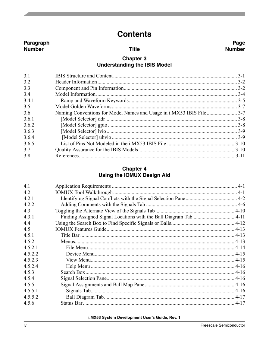
Paragraph Number Contents Title Chapter 3 Understanding the IBIS Model Page Number 3.1 3.2 3.3 3.4 3.4.1 3.5 3.6 3.6.1 3.6.2 3.6.3 3.6.4 3.6.5 3.7 3.8 4.1 4.2 4.2.1 4.2.2 4.3 4.3.1 4.4 4.5 4.5.1 4.5.2 4.5.2.1 4.5.2.2 4.5.2.3 4.5.2.4 4.5.3 4.5.4 4.5.5 4.5.5.1 4.5.5.2 4.5.6 iv IBIS Structure and Content.............................................................................................. 3-1 Header Information.......................................................................................................... 3-2 Component and Pin Information...................................................................................... 3-2 Model Information........................................................................................................... 3-4 Ramp and Waveform Keywords.................................................................................. 3-5 Model Golden Waveforms............................................................................................... 3-7 Naming Conventions for Model Names and Usage in i.MX53 IBIS File....................... 3-7 [Model Selector] ddr.................................................................................................... 3-8 [Model Selector] gpio .................................................................................................. 3-8 [Model Selector] lvio................................................................................................... 3-9 [Model Selector] uhvio ............................................................................................... 3-9 List of Pins Not Modeled in the i.MX53 IBIS File ................................................... 3-10 Quality Assurance for the IBIS Models......................................................................... 3-10 References...................................................................................................................... 3-11 Chapter 4 Using the IOMUX Design Aid Application Requirements ............................................................................................... 4-1 IOMUX Tool Walkthrough.............................................................................................. 4-1 Identifying Signal Conflicts with the Signal Selection Pane....................................... 4-2 Adding Comments with the Signals Tab ..................................................................... 4-6 Toggling the Alternate View of the Signals Tab............................................................ 4-10 Finding Assigned Signal Locations with the Ball Diagram Tab ............................... 4-11 Using the Search Box to Find Specific Signals or Balls................................................ 4-12 IOMUX Features Guide................................................................................................. 4-13 Title Bar ..................................................................................................................... 4-13 Menus......................................................................................................................... 4-13 File Menu............................................................................................................... 4-14 Device Menu.......................................................................................................... 4-15 View Menu............................................................................................................. 4-15 Help Menu ............................................................................................................. 4-16 Search Box................................................................................................................. 4-16 Signal Selection Pane................................................................................................. 4-16 Signal Assignments and Ball Map Pane.................................................................... 4-16 Signals Tab............................................................................................................. 4-16 Ball Diagram Tab................................................................................................... 4-17 Status Bar................................................................................................................... 4-17 i.MX53 System Development User’s Guide, Rev. 1 Freescale Semiconductor
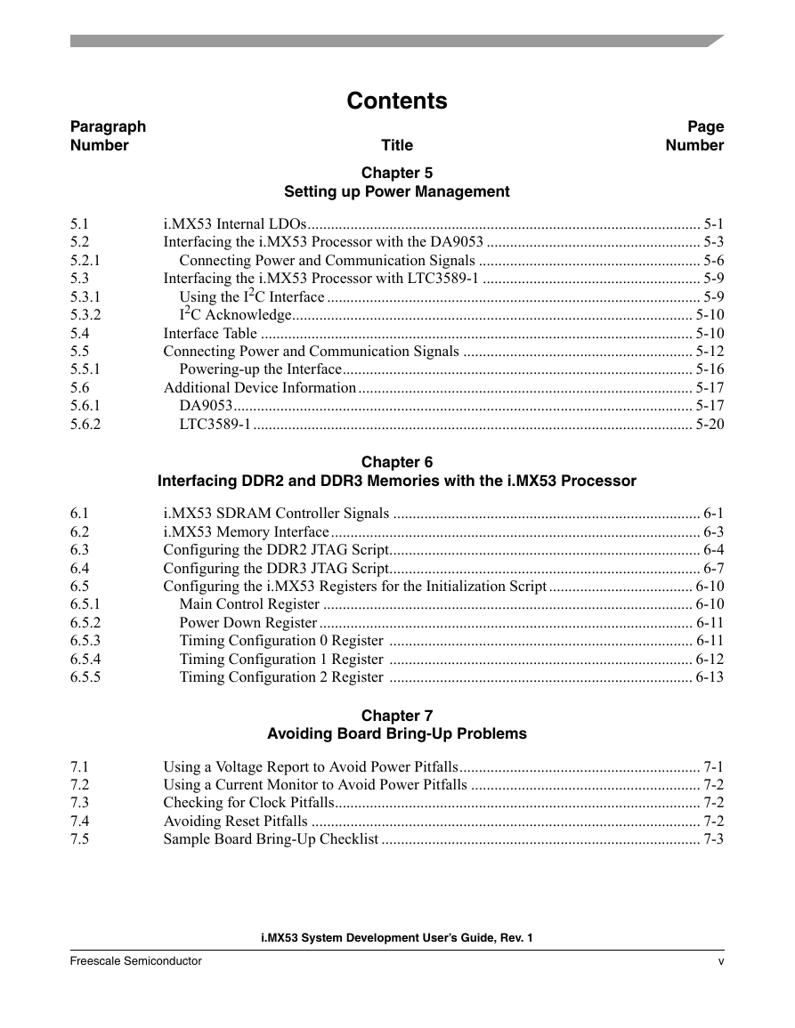
Paragraph Number Contents Title Chapter 5 Setting up Power Management Page Number 5.1 5.2 5.2.1 5.3 5.3.1 5.3.2 5.4 5.5 5.5.1 5.6 5.6.1 5.6.2 6.1 6.2 6.3 6.4 6.5 6.5.1 6.5.2 6.5.3 6.5.4 6.5.5 7.1 7.2 7.3 7.4 7.5 i.MX53 Internal LDOs..................................................................................................... 5-1 Interfacing the i.MX53 Processor with the DA9053 ....................................................... 5-3 Connecting Power and Communication Signals ......................................................... 5-6 Interfacing the i.MX53 Processor with LTC3589-1 ........................................................ 5-9 Using the I2C Interface ................................................................................................ 5-9 I2C Acknowledge....................................................................................................... 5-10 Interface Table ............................................................................................................... 5-10 Connecting Power and Communication Signals ........................................................... 5-12 Powering-up the Interface.......................................................................................... 5-16 Additional Device Information...................................................................................... 5-17 DA9053...................................................................................................................... 5-17 LTC3589-1................................................................................................................. 5-20 Interfacing DDR2 and DDR3 Memories with the i.MX53 Processor Chapter 6 i.MX53 SDRAM Controller Signals ............................................................................... 6-1 i.MX53 Memory Interface............................................................................................... 6-3 Configuring the DDR2 JTAG Script................................................................................ 6-4 Configuring the DDR3 JTAG Script................................................................................ 6-7 Configuring the i.MX53 Registers for the Initialization Script ..................................... 6-10 Main Control Register ............................................................................................... 6-10 Power Down Register ................................................................................................ 6-11 Timing Configuration 0 Register .............................................................................. 6-11 Timing Configuration 1 Register .............................................................................. 6-12 Timing Configuration 2 Register .............................................................................. 6-13 Chapter 7 Avoiding Board Bring-Up Problems Using a Voltage Report to Avoid Power Pitfalls.............................................................. 7-1 Using a Current Monitor to Avoid Power Pitfalls ........................................................... 7-2 Checking for Clock Pitfalls.............................................................................................. 7-2 Avoiding Reset Pitfalls .................................................................................................... 7-2 Sample Board Bring-Up Checklist .................................................................................. 7-3 Freescale Semiconductor v i.MX53 System Development User’s Guide, Rev. 1
Paragraph Number Contents Title Chapter 8 Using the Clock Connectivity Table Chapter 9 Configuring JTAG Tools for Debugging Page Number 9.1 9.2 Accessing Debug with a JTAG Scan Chain (ARM tools) ............................................... 9-1 Accessing Debug with a JTAG Scan Chain (other JTAG tools)...................................... 9-4 Porting the On-Board-Diagnostic-Suite (OBDS) to a Custom Board Chapter 10 Supported Components.................................................................................................. 10-1 Customizing OBDS for Specific Hardware................................................................... 10-2 UART (serial port) Test ............................................................................................. 10-2 DDR Test ................................................................................................................... 10-2 Audio Test.................................................................................................................. 10-3 IPU Display Test........................................................................................................ 10-3 I2C Test ...................................................................................................................... 10-3 SD/MMC Test............................................................................................................ 10-3 LED Test.................................................................................................................... 10-3 Ethernet (FEC) Loopback Test .................................................................................. 10-4 SPI-NOR Test ............................................................................................................ 10-4 Porting U-Boot from an i.MX53 Reference Board to an i.MX53 Custom Board Chapter 11 Obtaining the Source Code for the U-Boot ................................................................... 11-1 Preparing the Code......................................................................................................... 11-1 Customizing the i.MX53 Custom Board Code.............................................................. 11-2 Changing the DCD Table for i.MX53 DDR3 Initialization....................................... 11-3 Booting with the Modified U-Boot ........................................................................... 11-3 Further Customization at System Boot...................................................................... 11-3 Customizing the Printed Board Name ....................................................................... 11-4 Chapter 12 Porting the Android Kernel Patching the Android Kernel ......................................................................................... 12-1 Configuring Android Release for Customized Platforms.............................................. 12-1 Enabling and Disabling Default Resources ............................................................... 12-2 i.MX53 System Development User’s Guide, Rev. 1 Freescale Semiconductor 10.1 10.2 10.2.1 10.2.2 10.2.3 10.2.4 10.2.5 10.2.6 10.2.7 10.2.8 10.2.9 11.1 11.2 11.3 11.3.1 11.3.2 11.3.3 11.3.4 12.1 12.2 12.2.1 vi
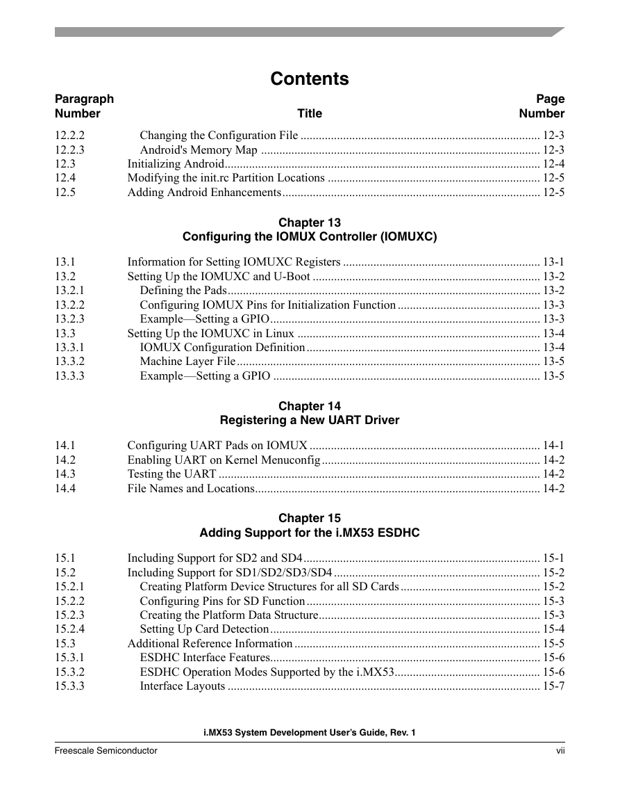
Contents Paragraph Number 12.2.2 12.2.3 12.3 12.4 12.5 Title Page Number Changing the Configuration File ............................................................................... 12-3 Android's Memory Map ............................................................................................ 12-3 Initializing Android........................................................................................................ 12-4 Modifying the init.rc Partition Locations ...................................................................... 12-5 Adding Android Enhancements..................................................................................... 12-5 Configuring the IOMUX Controller (IOMUXC) Chapter 13 Information for Setting IOMUXC Registers ................................................................. 13-1 Setting Up the IOMUXC and U-Boot ........................................................................... 13-2 Defining the Pads....................................................................................................... 13-2 Configuring IOMUX Pins for Initialization Function ............................................... 13-3 Example—Setting a GPIO......................................................................................... 13-3 Setting Up the IOMUXC in Linux ................................................................................ 13-4 IOMUX Configuration Definition............................................................................. 13-4 Machine Layer File.................................................................................................... 13-5 Example—Setting a GPIO ........................................................................................ 13-5 Chapter 14 Registering a New UART Driver Configuring UART Pads on IOMUX ............................................................................ 14-1 Enabling UART on Kernel Menuconfig........................................................................ 14-2 Testing the UART .......................................................................................................... 14-2 File Names and Locations.............................................................................................. 14-2 Chapter 15 Adding Support for the i.MX53 ESDHC Including Support for SD2 and SD4.............................................................................. 15-1 Including Support for SD1/SD2/SD3/SD4.................................................................... 15-2 Creating Platform Device Structures for all SD Cards.............................................. 15-2 Configuring Pins for SD Function............................................................................. 15-3 Creating the Platform Data Structure......................................................................... 15-3 Setting Up Card Detection......................................................................................... 15-4 Additional Reference Information ................................................................................. 15-5 ESDHC Interface Features......................................................................................... 15-6 ESDHC Operation Modes Supported by the i.MX53................................................ 15-6 Interface Layouts ....................................................................................................... 15-7 13.1 13.2 13.2.1 13.2.2 13.2.3 13.3 13.3.1 13.3.2 13.3.3 14.1 14.2 14.3 14.4 15.1 15.2 15.2.1 15.2.2 15.2.3 15.2.4 15.3 15.3.1 15.3.2 15.3.3 Freescale Semiconductor vii i.MX53 System Development User’s Guide, Rev. 1
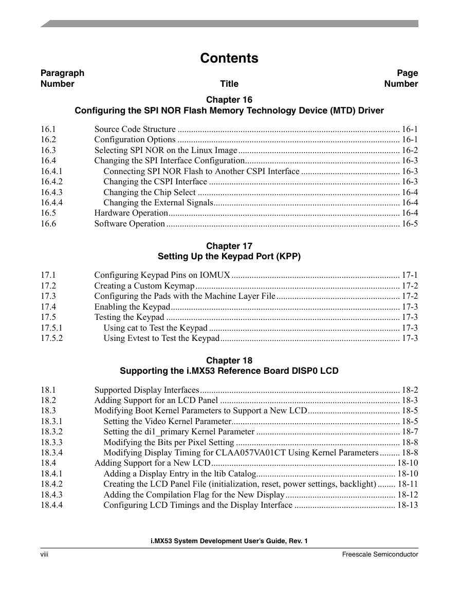
Paragraph Number Contents Title Page Number Configuring the SPI NOR Flash Memory Technology Device (MTD) Driver Chapter 16 Source Code Structure ................................................................................................... 16-1 Configuration Options ................................................................................................... 16-1 Selecting SPI NOR on the Linux Image........................................................................ 16-2 Changing the SPI Interface Configuration..................................................................... 16-3 Connecting SPI NOR Flash to Another CSPI Interface ............................................ 16-3 Changing the CSPI Interface ..................................................................................... 16-3 Changing the Chip Select .......................................................................................... 16-4 Changing the External Signals................................................................................... 16-4 Hardware Operation....................................................................................................... 16-4 Software Operation ........................................................................................................ 16-5 Chapter 17 Setting Up the Keypad Port (KPP) Configuring Keypad Pins on IOMUX ........................................................................... 17-1 Creating a Custom Keymap........................................................................................... 17-2 Configuring the Pads with the Machine Layer File....................................................... 17-2 Enabling the Keypad...................................................................................................... 17-3 Testing the Keypad ........................................................................................................ 17-3 Using cat to Test the Keypad ..................................................................................... 17-3 Using Evtest to Test the Keypad................................................................................ 17-3 Supporting the i.MX53 Reference Board DISP0 LCD Chapter 18 Supported Display Interfaces......................................................................................... 18-2 Adding Support for an LCD Panel ................................................................................ 18-3 Modifying Boot Kernel Parameters to Support a New LCD......................................... 18-5 Setting the Video Kernel Parameter........................................................................... 18-5 Setting the di1_primary Kernel Parameter ................................................................ 18-7 Modifying the Bits per Pixel Setting ......................................................................... 18-8 Modifying Display Timing for CLAA057VA01CT Using Kernel Parameters ......... 18-8 Adding Support for a New LCD.................................................................................. 18-10 Adding a Display Entry in the ltib Catalog.............................................................. 18-10 Creating the LCD Panel File (initialization, reset, power settings, backlight) ........ 18-11 Adding the Compilation Flag for the New Display................................................. 18-12 Configuring LCD Timings and the Display Interface ............................................. 18-13 i.MX53 System Development User’s Guide, Rev. 1 Freescale Semiconductor 16.1 16.2 16.3 16.4 16.4.1 16.4.2 16.4.3 16.4.4 16.5 16.6 17.1 17.2 17.3 17.4 17.5 17.5.1 17.5.2 18.1 18.2 18.3 18.3.1 18.3.2 18.3.3 18.3.4 18.4 18.4.1 18.4.2 18.4.3 18.4.4 viii
分享到:
收藏