LTC4218
Hot Swap Controller
DESCRIPTION
The LTC®4218 is a Hot Swap™ controller that allows a board
to be safely inserted and removed from a live backplane.
An internal high side switch driver controls the gate of an
external N-channel MOSFET for supply voltages from 2.9V
to 26.5V. A dedicated 12V version (LTC4218-12) contains
preset 12V specifi c thresholds, while the standard LTC4218
allows adjustable thresholds.
The LTC4218 provides an accurate (5%) current limit with
current foldback limiting. The current limit threshold can
be adjusted dynamically using an external pin. Additional
features include a current monitor output that amplifi es
the sense voltage for ground referenced current sensing.
Overvoltage, undervoltage and power good monitoring
are also provided.
L, LT, LTC, LTM, Linear Technology and the Linear logo are registered trademarks and
Hot Swap is a trademark of Linear Technology Corporation. All other trademarks are the
property of their respective owners.
FEATURES
n Wide Operating Voltage Range: 2.9V to 26.5V
n Adjustable, 5% Accurate (15mV) Current Limit
n Current Monitor Output
n Adjustable Current Limit Timer Before Fault
n Power Good and Fault Outputs
n Adjustable Inrush Current Control
n 2% Accurate Undervoltage and Overvoltage
n Available in 16-Lead SSOP and 16-Pin 5mm × 3mm
Protection
DFN Packages
APPLICATIONS
n RAID Systems
n ATCA, AMC, μTCA Systems
n Server I/O Cards
n Industrial
TYPICAL APPLICATION
12V, 6A Card Resident Application
Power-Up Waveform
12V
2mΩ
Si7108DN
10Ω
VOUT
12V
6A
330μF
+
SENSE– GATE
SENSE+
VDD
UV
LTC4218DHC-12
SOURCE
1k
0.01μF
12V
10k
VIN
10V/DIV
IIN
1A/DIV
VOUT
10V/DIV
PG
10V/DIV
AUTO
RETRY
0.1μF
0.1μF
FLT
TIMER
INTVCC
PG
IMON
GND
20k
ADC
4218 TA01a
25ms/DIV
4218 TA01b
4218fe
1
�
LTC4218
(Notes 1, 2)
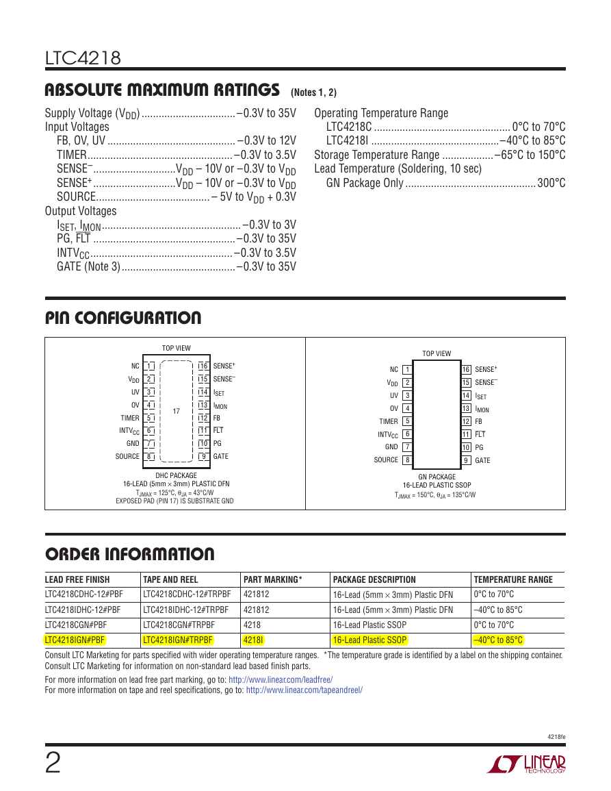
ABSOLUTE MAXIMUM RATINGS
Supply Voltage (VDD) .................................–0.3V to 35V
Input Voltages
FB, OV, UV ............................................. –0.3V to 12V
TIMER ................................................... –0.3V to 3.5V
SENSE– .............................VDD – 10V or –0.3V to VDD
SENSE+ .............................VDD – 10V or –0.3V to VDD
SOURCE ........................................ – 5V to VDD + 0.3V
Operating Temperature Range
LTC4218C ................................................ 0°C to 70°C
LTC4218I .............................................–40°C to 85°C
Storage Temperature Range ..................–65°C to 150°C
Lead Temperature (Soldering, 10 sec)
GN Package Only ..............................................300°C
NC
VDD
UV
OV
TIMER
INTVCC
GND
SOURCE
1
2
3
4
5
6
7
8
TOP VIEW
16
15
14
13
12
11
10
9
SENSE+
SENSE–
ISET
IMON
FB
FLT
PG
GATE
GN PACKAGE
16-LEAD PLASTIC SSOP
TJMAX = 150°C, θJA = 135°C/W
Output Voltages
ISET, IMON ................................................. –0.3V to 3V
PG, FLT ..................................................–0.3V to 35V
INTVCC .................................................. –0.3V to 3.5V
GATE (Note 3) ........................................–0.3V to 35V
PIN CONFIGURATION
TOP VIEW
17
16
15
14
13
12
11
10
9
SENSE+
SENSE–
ISET
IMON
FB
FLT
PG
GATE
NC
VDD
UV
OV
TIMER
INTVCC
GND
SOURCE
1
2
3
4
5
6
7
8
DHC PACKAGE
16-LEAD (5mm 3mm) PLASTIC DFN
TJMAX = 125°C, θJA = 43°C/W
EXPOSED PAD (PIN 17) IS SUBSTRATE GND
ORDER INFORMATION
LEAD FREE FINISH
LTC4218CDHC-12#PBF
LTC4218IDHC-12#PBF
LTC4218CGN#PBF
LTC4218IGN#PBF
Consult LTC Marketing for parts specifi ed with wider operating temperature ranges. *The temperature grade is identifi ed by a label on the shipping container.
Consult LTC Marketing for information on non-standard lead based fi nish parts.
For more information on lead free part marking, go to: http://www.linear.com/leadfree/
For more information on tape and reel specifi cations, go to: http://www.linear.com/tapeandreel/
PACKAGE DESCRIPTION
16-Lead (5mm × 3mm) Plastic DFN
16-Lead (5mm × 3mm) Plastic DFN
16-Lead Plastic SSOP
16-Lead Plastic SSOP
TAPE AND REEL
LTC4218CDHC-12#TRPBF
LTC4218IDHC-12#TRPBF
LTC4218CGN#TRPBF
LTC4218IGN#TRPBF
TEMPERATURE RANGE
0°C to 70°C
–40°C to 85°C
0°C to 70°C
–40°C to 85°C
PART MARKING*
421812
421812
4218
4218I
2
4218fe
�
The l denotes the specifi cations which apply over the full operating
PARAMETER
CONDITIONS
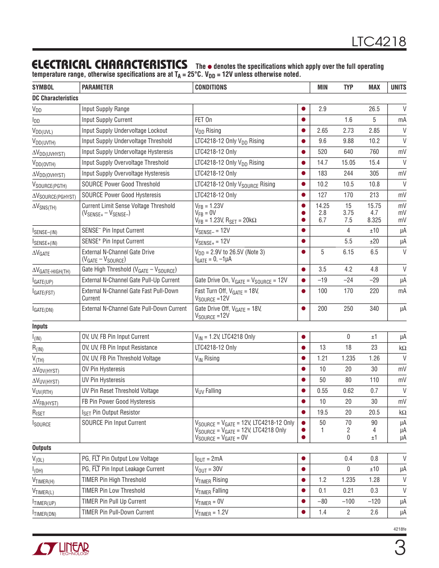
ELECTRICAL CHARACTERISTICS
temperature range, otherwise specifi cations are at TA = 25°C. VDD = 12V unless otherwise noted.
SYMBOL
DC Characteristics
Input Supply Range
VDD
Input Supply Current
IDD
Input Supply Undervoltage Lockout
VDD(UVL)
Input Supply Undervoltage Threshold
VDD(UVTH)
ΔVDD(UVHYST)
Input Supply Undervoltage Hysteresis
Input Supply Overvoltage Threshold
VDD(OVTH)
ΔVDD(OVHYST)
Input Supply Overvoltage Hysteresis
SOURCE Power Good Threshold
VSOURCE(PGTH)
ΔVSOURCE(PGHYST) SOURCE Power Good Hysteresis
ΔVSNS(TH)
FET On
VDD Rising
LTC4218-12 Only VDD Rising
LTC4218-12 Only
LTC4218-12 Only VDD Rising
LTC4218-12 Only
LTC4218-12 Only VSOURCE Rising
LTC4218-12 Only
VFB = 1.23V
VFB = 0V
VFB = 1.23V, RSET = 20kΩ
VSENSE– = 12V
VSENSE+ = 12V
VDD = 2.9V to 26.5V (Note 3)
IGATE = 0, –1μA
Gate Drive On, VGATE = VSOURCE = 12V
Fast Turn Off, VGATE = 18V,
VSOURCE =12V
Gate Drive Off, VGATE = 18V,
VSOURCE =12V
VIN = 1.2V, LTC4218 Only
LTC4218-12 Only
VIN Rising
VUV Falling
VSOURCE = VGATE = 12V, LTC4218-12 Only
VSOURCE = VGATE = 12V, LTC4218 Only
VSOURCE = VGATE = 0V
Current Limit Sense Voltage Threshold
(VSENSE+ – VSENSE–)
SENSE– Pin Input Current
SENSE+ Pin Input Current
External N-Channel Gate Drive
(VGATE – VSOURCE)
Gate High Threshold (VGATE – VSOURCE)
External N-Channel Gate Pull-Up Current
External N-Channel Gate Fast Pull-Down
Current
External N-Channel Gate Pull-Down Current
OV, UV, FB Pin Input Current
OV, UV, FB Pin Input Resistance
OV, UV, FB Pin Threshold Voltage
OV Pin Hysteresis
UV Pin Hysteresis
UV Pin Reset Threshold Voltage
FB Pin Power Good Hysteresis
ISET Pin Output Resistor
SOURCE Pin Input Current
LTC4218
MIN
TYP
MAX
UNITS
l
l
l
l
l
l
l
l
l
l
l
l
l
l
l
l
l
l
l
l
l
l
l
l
l
l
l
l
l
l
l
l
l
l
l
l
2.9
2.65
9.6
520
14.7
183
10.2
127
14.25
2.8
6.7
5
3.5
–19
100
200
13
1.21
10
50
0.55
10
19.5
50
1
1.2
0.1
–80
1.4
26.5
5
2.85
10.2
760
15.4
305
10.8
213
15.75
4.7
8.325
±10
±20
6.5
4.8
–29
220
340
±1
23
1.26
30
110
0.7
30
20.5
90
4
±1
0.8
±10
1.28
0.3
–120
2.6
1.6
2.73
9.88
640
15.05
244
10.5
170
15
3.75
7.5
4
5.5
6.15
4.2
–24
170
250
0
18
1.235
20
80
0.62
20
20
70
2
0
0.4
0
1.235
0.21
–100
2
V
mA
V
V
mV
V
mV
V
mV
mV
mV
mV
μA
μA
V
V
μA
mA
μA
μA
kΩ
V
mV
mV
V
mV
kΩ
μA
μA
μA
V
μA
V
V
μA
μA
4218fe
3
ISENSE–(IN)
ISENSE+(IN)
ΔVGATE
ΔVGATE-HIGH(TH)
IGATE(UP)
IGATE(FST)
IGATE(DN)
Inputs
I(IN)
R(IN)
V(TH)
ΔVOV(HYST)
ΔVUV(HYST)
VUV(RTH)
ΔVFB(HYST)
RISET
ISOURCE
Outputs
V(OL)
I(OH)
VTIMER(H)
VTIMER(L)
ITIMER(UP)
ITIMER(DN)
PG, FLT Pin Output Low Voltage
PG, FLT Pin Input Leakage Current
TIMER Pin High Threshold
TIMER Pin Low Threshold
TIMER Pin Pull Up Current
TIMER Pin Pull-Down Current
IOUT = 2mA
VOUT = 30V
VTIMER Rising
VTIMER Falling
VTIMER = 0V
VTIMER = 1.2V
�
LTC4218
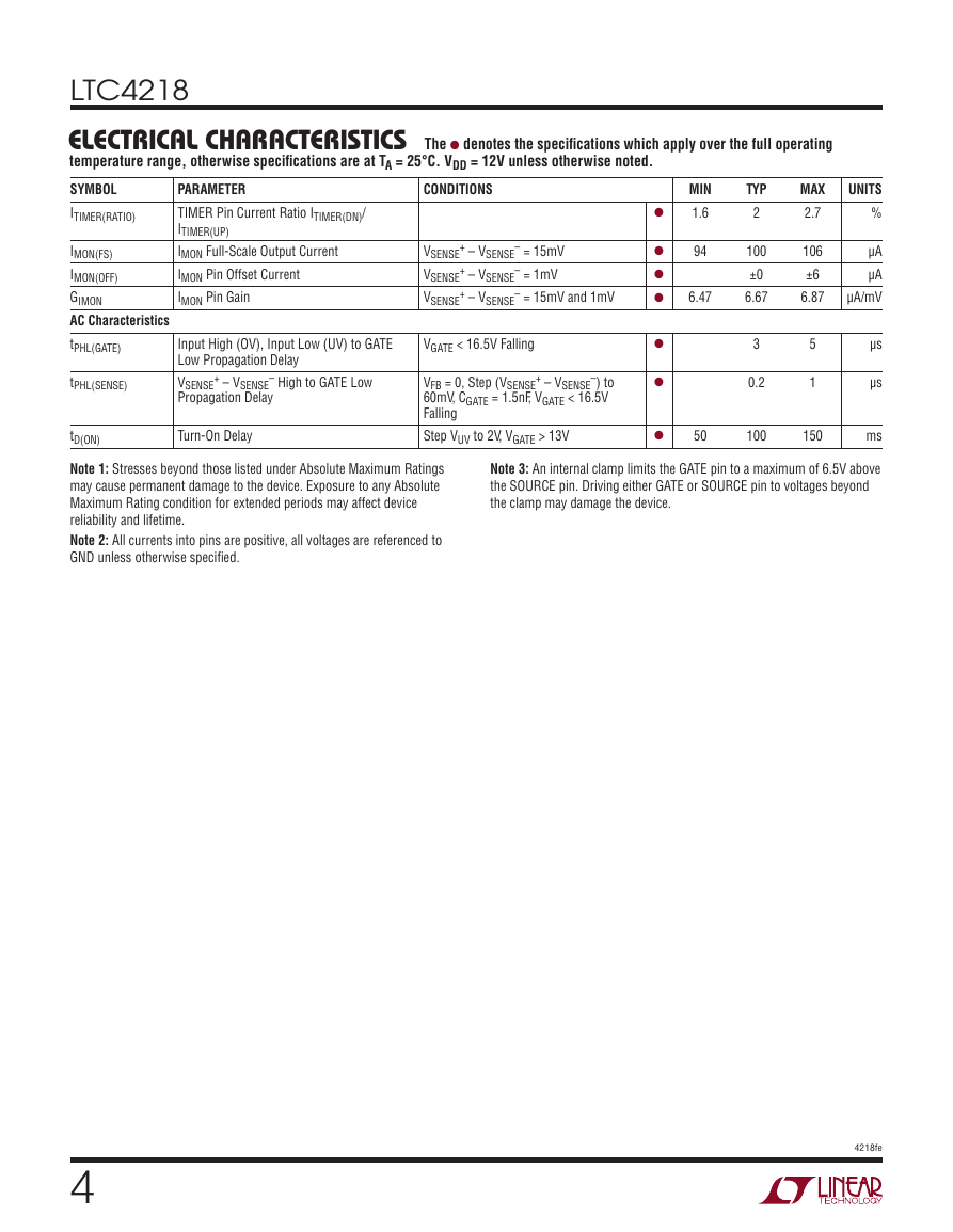
ELECTRICAL CHARACTERISTICS
temperature range, otherwise specifi cations are at TA = 25°C. VDD = 12V unless otherwise noted.
SYMBOL
ITIMER(RATIO)
CONDITIONS
The l denotes the specifi cations which apply over the full operating
PARAMETER
TIMER Pin Current Ratio ITIMER(DN)/
ITIMER(UP)
IMON Full-Scale Output Current
IMON Pin Offset Current
IMON Pin Gain
Input High (OV), Input Low (UV) to GATE
Low Propagation Delay
+ – VSENSE
VSENSE
Propagation Delay
– High to GATE Low
IMON(FS)
IMON(OFF)
GIMON
AC Characteristics
tPHL(GATE)
tPHL(SENSE)
tD(ON)
Turn-On Delay
VSENSE
VSENSE
VSENSE
+ – VSENSE
+ – VSENSE
+ – VSENSE
– = 15mV
– = 1mV
– = 15mV and 1mV
VGATE < 16.5V Falling
+ – VSENSE
–) to
VFB = 0, Step (VSENSE
60mV, CGATE = 1.5nF, VGATE < 16.5V
Falling
Step VUV to 2V, VGATE > 13V
MIN
1.6
94
6.47
TYP
2
100
±0
6.67
3
0.2
MAX
2.7
106
±6
6.87
5
1
UNITS
%
μA
μA
μA/mV
μs
μs
50
100
150
ms
l
l
l
l
l
l
l
Note 1: Stresses beyond those listed under Absolute Maximum Ratings
may cause permanent damage to the device. Exposure to any Absolute
Maximum Rating condition for extended periods may affect device
reliability and lifetime.
Note 2: All currents into pins are positive, all voltages are referenced to
GND unless otherwise specifi ed.
Note 3: An internal clamp limits the GATE pin to a maximum of 6.5V above
the SOURCE pin. Driving either GATE or SOURCE pin to voltages beyond
the clamp may damage the device.
4
4218fe
�
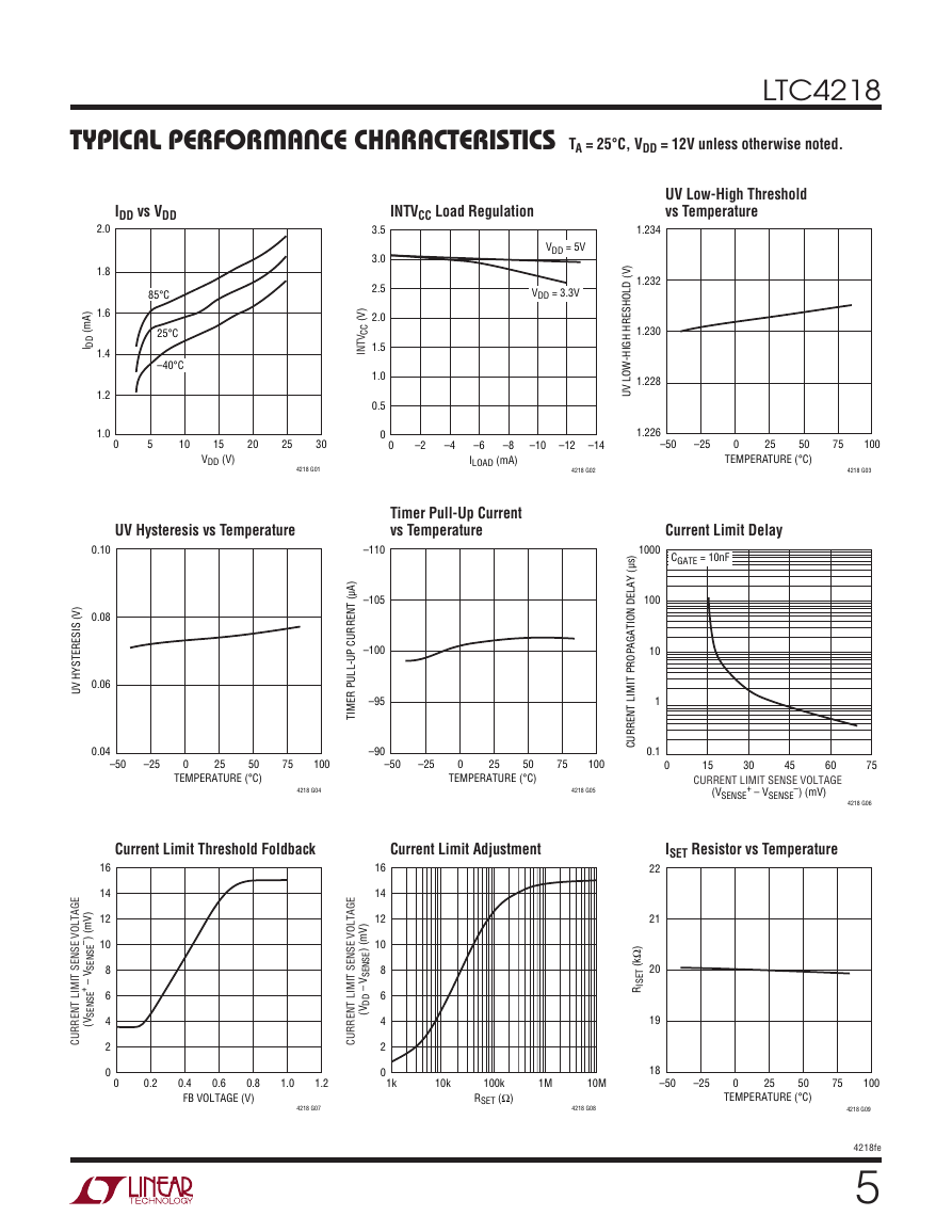
TYPICAL PERFORMANCE CHARACTERISTICS
TA = 25°C, VDD = 12V unless otherwise noted.
LTC4218
2.0
1.8
)
A
m
(
D
D
I
1.6
1.4
IDD vs VDD
85°C
25°C
–40°C
1.2
1.0
0
INTVCC Load Regulation
VDD = 5V
VDD = 3.3V
3.5
3.0
2.5
2.0
1.5
1.0
0.5
)
V
(
C
C
V
T
N
I
UV Low-High Threshold
vs Temperature
1.234
1.232
1.230
1.228
)
V
(
D
L
O
H
S
E
R
H
H
G
H
-
W
O
L
V
U
I
5
10
15
20
25
30
VDD (V)
4218 G01
0
0
–2
–4
–8
–6
ILOAD (mA)
–10
–12
–14
4218 G02
1.226
–50
–25
0
25
50
TEMPERATURE (°C)
75
100
4218 G03
UV Hysteresis vs Temperature
Timer Pull-Up Current
vs Temperature
0.10
0.08
0.06
)
V
(
S
I
S
E
R
E
T
S
Y
H
V
U
0.04
–50
–25
–110
–105
–100
–95
)
A
μ
(
T
N
E
R
R
U
C
P
U
-
L
L
U
P
R
E
M
I
T
0
25
50
TEMPERATURE (°C)
–90
–50
–25
75
100
4218 G04
0
25
50
TEMPERATURE (°C)
)
s
μ
(
Y
A
L
E
D
N
O
I
T
A
G
A
P
O
R
P
T
I
M
I
L
T
N
E
R
R
U
C
75
100
4218 G05
Current Limit Delay
CGATE = 10nF
1000
100
10
1
0.1
0
15
30
45
60
75
CURRENT LIMIT SENSE VOLTAGE
(VSENSE
+ – VSENSE
–) (mV)
4218 G06
Current Limit Threshold Foldback
Current Limit Adjustment
)
V
m
(
)
–
E
G
A
T
L
O
V
E
S
N
E
S
T
I
M
I
L
T
N
E
R
R
U
C
E
S
N
E
S
V
–
E
S
N
E
S
V
(
+
16
14
12
10
8
6
4
2
0
0
0.2
0.6
0.4
0.8
FB VOLTAGE (V)
1.0
1.2
4218 G07
E
G
A
T
L
O
V
E
S
N
E
S
T
I
M
I
L
T
N
E
R
R
U
C
)
V
m
(
)
E
S
N
E
S
V
–
D
D
V
(
16
14
12
10
8
6
4
2
0
ISET Resistor vs Temperature
22
21
20
19
)
Ω
k
(
T
E
S
R
I
1k
10k
100k
RSET (Ω)
1M
10M
4218 G08
18
–50
–25
0
25
50
TEMPERATURE (°C)
75
100
4218 G09
4218fe
5
�
LTC4218
TYPICAL PERFORMANCE CHARACTERISTICS
TA = 25°C, VDD = 12V unless otherwise noted.
GATE Pull-Up Current
vs Temperature
Gate Pull-Up Current
vs Gate Drive
VDD = 12V
VDD = 3.3V
0
–5
–10
–15
–20
–25
–30
IGATE (μA)
4218 G11
PG, FLT VOUT Low vs ILOAD
PG
FLT
)
V
(
)
E
C
R
U
O
S
V
–
E
T
A
G
V
(
I
E
V
R
D
E
T
A
G
Gate Drive vs VDD
6.2
6.0
5.8
5.6
5.4
5.2
0
5
10
15
20
25
30
VDD (V)
4218 G12
IMON vs Temperature and VDD
VDD = 3.3V, 12V, 24V
VSENSE
+ – VSENSE
– = 15mV
105
100
95
90
85
)
A
μ
(
N
O
M
I
0
2
4
6
8
10
12
ILOAD (mA)
4218 G14
80
–50
–25
0
25
50
TEMPERATURE (°C)
VIMON vs Sense
4
3
2
1
)
V
(
N
O
M
V
I
RIMON = 100k
RIMON = 40k
RIMON = 20k
RIMON = 10k
75
100
4218 G15
4218fe
–26.0
–25.5
–25.0
–24.5
)
A
μ
(
P
U
-
L
L
U
P
E
T
A
G
I
–24.0
–50
–25
0
25
50
TEMPERATURE (°C)
Gate Drive vs Temperature
6.15
6.14
6.13
6.12
6.11
)
V
(
)
E
C
R
U
O
S
V
–
E
T
A
G
V
(
E
V
I
R
D
E
T
A
G
6.10
–50
–25
0
25
50
TEMPERATURE (°C)
7
6
5
4
3
2
1
0
14
12
10
8
6
4
2
0
)
V
(
)
E
C
R
U
O
S
V
–
E
T
A
G
V
(
I
E
V
R
D
E
T
A
G
75
100
4218 G10
)
V
(
W
O
L
T
U
O
V
T
L
F
,
G
P
75
100
4218 G13
IMON vs Sense
100
)
A
μ
(
N
O
M
I
75
50
25
0
0
6
5
10
SENSE VOLTAGE (mV)
15
4218 G16
0
0
5
10
SENSE VOLTAGE (mV)
15
4218 G17
�
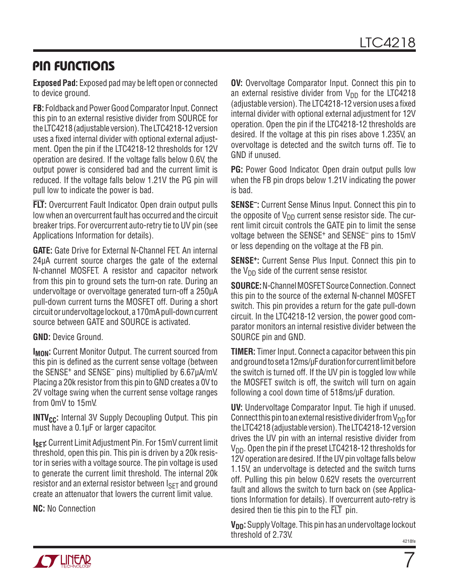
PIN FUNCTIONS
Exposed Pad: Exposed pad may be left open or connected
to device ground.
FB: Foldback and Power Good Comparator Input. Connect
this pin to an external resistive divider from SOURCE for
the LTC4218 (adjustable version). The LTC4218-12 version
uses a fi xed internal divider with optional external adjust-
ment. Open the pin if the LTC4218-12 thresholds for 12V
operation are desired. If the voltage falls below 0.6V, the
output power is considered bad and the current limit is
reduced. If the voltage falls below 1.21V the PG pin will
pull low to indicate the power is bad.
FLT: Overcurrent Fault Indicator. Open drain output pulls
low when an overcurrent fault has occurred and the circuit
breaker trips. For overcurrent auto-retry tie to UV pin (see
Applications Information for details).
GATE: Gate Drive for External N-Channel FET. An internal
24μA current source charges the gate of the external
N-channel MOSFET. A resistor and capacitor network
from this pin to ground sets the turn-on rate. During an
undervoltage or overvoltage generated turn-off a 250μA
pull-down current turns the MOSFET off. During a short
circuit or undervoltage lockout, a 170mA pull-down current
source between GATE and SOURCE is activated.
GND: Device Ground.
IMON: Current Monitor Output. The current sourced from
this pin is defi ned as the current sense voltage (between
the SENSE+ and SENSE– pins) multiplied by 6.67μA/mV.
Placing a 20k resistor from this pin to GND creates a 0V to
2V voltage swing when the current sense voltage ranges
from 0mV to 15mV.
INTVCC: Internal 3V Supply Decoupling Output. This pin
must have a 0.1μF or larger capacitor.
ISET: Current Limit Adjustment Pin. For 15mV current limit
threshold, open this pin. This pin is driven by a 20k resis-
tor in series with a voltage source. The pin voltage is used
to generate the current limit threshold. The internal 20k
resistor and an external resistor between ISET and ground
create an attenuator that lowers the current limit value.
NC: No Connection
LTC4218
OV: Overvoltage Comparator Input. Connect this pin to
an external resistive divider from VDD for the LTC4218
(adjustable version). The LTC4218-12 version uses a fi xed
internal divider with optional external adjustment for 12V
operation. Open the pin if the LTC4218-12 thresholds are
desired. If the voltage at this pin rises above 1.235V, an
overvoltage is detected and the switch turns off. Tie to
GND if unused.
PG: Power Good Indicator. Open drain output pulls low
when the FB pin drops below 1.21V indicating the power
is bad.
SENSE–: Current Sense Minus Input. Connect this pin to
the opposite of VDD current sense resistor side. The cur-
rent limit circuit controls the GATE pin to limit the sense
voltage between the SENSE+ and SENSE– pins to 15mV
or less depending on the voltage at the FB pin.
SENSE+: Current Sense Plus Input. Connect this pin to
the VDD side of the current sense resistor.
SOURCE: N-Channel MOSFET Source Connection. Connect
this pin to the source of the external N-channel MOSFET
switch. This pin provides a return for the gate pull-down
circuit. In the LTC4218-12 version, the power good com-
parator monitors an internal resistive divider between the
SOURCE pin and GND.
TIMER: Timer Input. Connect a capacitor between this pin
and ground to set a 12ms/μF duration for current limit before
the switch is turned off. If the UV pin is toggled low while
the MOSFET switch is off, the switch will turn on again
following a cool down time of 518ms/μF duration.
UV: Undervoltage Comparator Input. Tie high if unused.
Connect this pin to an external resistive divider from VDD for
the LTC4218 (adjustable version). The LTC4218-12 version
drives the UV pin with an internal resistive divider from
VDD. Open the pin if the preset LTC4218-12 thresholds for
12V operation are desired. If the UV pin voltage falls below
1.15V, an undervoltage is detected and the switch turns
off. Pulling this pin below 0.62V resets the overcurrent
fault and allows the switch to turn back on (see Applica-
tions Information for details). If overcurrent auto-retry is
desired then tie this pin to the FLT pin.
VDD: Supply Voltage. This pin has an undervoltage lockout
threshold of 2.73V.
4218fe
7
�
LTC4218
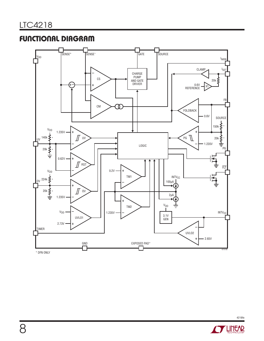
FUNCTIONAL DIAGRAM
VDD
SENSE+
SENSE–
GATE
SOURCE
–
+
CS
CM
UV
RST
OV
0.2V
UVLO1
1.235V
CHARGE
PUMP
AND GATE
DRIVER
LOGIC
+
–
+
–
TM1
TM2
INTVCC
100μA
2μA
VDD
3.1V
GEN
GND
EXPOSED PAD*
+–
+
–
+
–
+
–
–
+
VDD
1.235V
0.62V
1.235V
VDD
2.73V
140k
UV
20k
*
*
VDD
224k
OV
20k
*
*
TIMER
* DFN ONLY
CLAMP
20k
0.6V
REFERENCE
X1
IMON
ISET
FB
FOLDBACK
PG
+
–
0.6V
SOURCE
150k
20k
1.235V
*
*
PG
FLT
UVLO2
–
+
2.65V
INTVCC
4218 BD
8
4218fe
�




 2023年江西萍乡中考道德与法治真题及答案.doc
 2012年重庆南川中考生物真题及答案.doc
 2013年江西师范大学地理学综合及文艺理论基础考研真题.doc
 2020年四川甘孜小升初语文真题及答案I卷.doc
 2020年注册岩土工程师专业基础考试真题及答案.doc
 2023-2024学年福建省厦门市九年级上学期数学月考试题及答案.doc
 2021-2022学年辽宁省沈阳市大东区九年级上学期语文期末试题及答案.doc
 2022-2023学年北京东城区初三第一学期物理期末试卷及答案.doc
 2018上半年江西教师资格初中地理学科知识与教学能力真题及答案.doc
 2012年河北国家公务员申论考试真题及答案-省级.doc
 2020-2021学年江苏省扬州市江都区邵樊片九年级上学期数学第一次质量检测试题及答案.doc
 2022下半年黑龙江教师资格证中学综合素质真题及答案.doc