2
IEEE TRANSACTIONS ON ANTENNAS AND PROPAGATION, VOL. "-29, NO. 1, JANUARY 1981
Microstrip Antenna Technology
KEITH R. CARVER, MEMBER, IEEE, AND JAMES w. MINK, MEMBER, IEEE
with the relation
resonant freqnency of
Absfruct-A survey of microstrip antenna elements is presented,
with emphasis on theoretical and practical design techniques.
Available substrate materials are reviewed along
between dielectric constant tolerance and
microstrip patches. Several theoretical analysis techniques are
summarized, including transmission-line
and modal-expansion
(cavity) techniques as well as numerical methods such as the method of
moments and fmite-element techniques. Practical procedures
are
given for both standard rectangular and circular patches, as well as
variations on those designs including circularly polarized microstrip
patches. The quality, bandwidth, and efficiency factors
of typical
patch designs are discussed. Microstrip dipole and
conformal
antennas are summarized. Finally, critical needs for fnrther research
and development for this antenna are identified.
T
INTRODUCTION
HE PURPOSES of this paper are to describe analytical and
experimental design approaches for microstrip antenna
the state
for the current
provide a reference
review of
as it affects the
describes several
of
relatively new
of
to a les-
This
elements, and to provide a comprehensive survey of the state
of microstrip antenna element technology. A companion
paper [ 1 ] discussed microstrip array design techniques. Taken
together, these papers
state of development of microstrip elements and arrays
elements at a time when advancements in this
technology are being reported primarily in a wide variety
technical reports and private communications, and
ser extent in this TRANSACTIONS and other journals.
paper begins with a
materials technology
antennas, and then
to the analysis of rectangular and circular
patches, as well as
patches of other shapes and microstrip dipoles. Design curves
are presented for both rectangular and circular patch shapes,
and for
A dis-
cussion of the bandwidth and efficiency of the elements is
presented with the patch size, shape, substrate thickness, and
material properties as parameters. Several practical techniques
are outlined for modifying
as conformal arrays, feeds for dishes,
purpose applications
dual-frequency communication systems, etc. The paper con-
cludes with suggestions for future critical needs in the further
development of the antenna.
design of microstrip
theoretical approaches
linearly and circularly polarized elements.
the basic element for such special
of printed circuit
The microstrip antenna concept dates
back about 26
years to work in the U.S.A. by Deschamps [ 21 and in France
by Gutton and Baissinot [ 3 ] . Shortly thereafter, Lewin [ 991
investigated radiation from stripline discontinuities. Additional
studies were undertaken in the late
studied basic rectangular and square configurations. However,
other than the
original Deschamps
1960's by Kaloi, who
report, work
was not
Manuscript received March 5, 1980; revised July 22, 1980.
K. R. Carver is with the Physical Science Laboratory, New Mexico
J. W. Mink is with the U.S. Army Research Office, Research Tri-
State University, Las Cruces, NM 80003.
angle Park, NC 27709.
early 1970's, when a con-
was patented by Munson
and several-wavelength long
reported in the literature until the
ducting strip radiator separated from a ground plane by a
[4]. This half-
dielectric substrate was described by Byron
wavelength wide
strip was fed
by coaxial connections at periodic intervals along both radiat-
ing edges, and was used as an array for Project Camel. Shortly
thereafter, a microstrip element
[SI and data on basic rectangular and circular microstrip
[ 6 ] . Weinschel [7] de-
patches were published by Howell
veloped several microstrip geometries
for use with cylindrical
S-band arrays on rockets. Sanford [ 81 showed that the micro-
strip element could be used
in conformal array designs for
L-band communication from a KC-135 aircraft to the ATS-6
satellite. Additional work on basic microstrip patch elements
was reported in 1975 by Garvin et d . [ 91, Howell [ 101,
Weinschel [ 111, and Janes and Wilson [ 121. The early work
by Munson on the development of microstrip antennas for use
on rockets and mis-
as low-profie flush-mounted antennas
siles showed that this was a practical concept for use in many
antenna system problems, and thereby
gave birth to a new
antenna industry.
Mathematical modeling
of the basic microstrip radiator
[ 131, [ 141. The radiation pattern
of transmission-
the center
of a
was initially carried out by the application
line analogies to simple rectangular patches fed at
of a radiating wall
circular patch was analyzed and measurements reported by
Carver [ 151. The first mathematical analysis of a wide variety
of microstrip patch shapes was published in 1977 by Lo e t d .
[ 161, who used the. modal-expansion technique
to analyze
rectangular, circular, semicircular, and triangular patch shapes.
Similar comprehensive reports on advanced analysis techniques
were published by Derneryd
[ 141, [ 171, Shen and
Long
[ 181, and Carver and Coffey
[ 191. By 1978 the microstrip
patch antenna was becoming much more widely known and
used in a variety
companied by increased attention
munity to improved mathematical models
used for design. In
October 1979, the
meeting devoted
designs, array configurations,
held at New Mexico State University (NMSU), Las Cruces,
under cosponsorship of
NMSU's Physical Science Laboratory [ 201.
was ac-
by the theoretical com-
to microstrip antenna materials, practical
of communication systems. This
the U.S. Army Research Office
first international
and theoretical
models was
which could be
and
The terms stripline and microstrip are often encountered
in the literature, in connection with both transmission lines
and antennas. A stripline or triplate device is a sandwich of
three parallel conducting layers separated
di-
electric substrates, the center conductor of which is analogous
to the center conductor of a coaxial transmission line. If the
to a resonant slot cut orthogonally
center conductor couples
in the upper conductor, the
device is said to be a stripline
on this
radiator [ 21.1. Although there are many variations
printed-circuit stripline slot antenna, these are outside
the
scope of this paper and will not be considered further.
by two thin
By contrast a microstrip device in
its simplest form con-
0018-926X/81/0100-0002$00.75 0 1981 IEEE
�
MICROSTRIP
CARVER AND MINK:
ANTENNA TECHNOLOGY
3
GROUND
PLANE
TOP
VIEW
TOP
VIEW
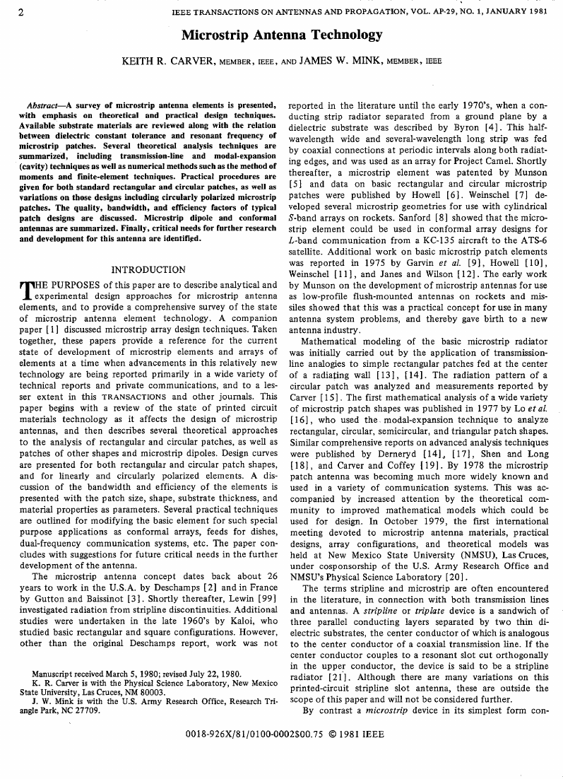
Fig. 1.
(a) Rectangular microstrip patch antenna. (b) Circular micro-
(d) Micro-
strip patch antenna. (c) Open-circuit microstrip radiator.
strip dipole antenna.
or circular patch, a resonant
sists of a sandwich of two parallel conducting layers separated
by a single thin dielectric substrate [ 221. The lowfr conductor
functions as a ground plane, and the upper conductor may be
a simple resonant rectangular
dipole, or a monolithically printed array of patches or dipoles
and the associated feed network. Since arrays of microstrip
patches and dipoles were considered in
the companion article
on microstrip arrays [ 11 , this paper will concentrate on basic
microstrip patches and dipoles. Fig. 1 shows a representative
collection of microstrip patch and dipole shapes and their
associated dielectric
microstrip antennas have been developed for use from
MHz to 38 GHz, and it can be expected that the technology
will soon extend to 60 GHz and beyond.
coupling between microstrip elements
where in [ 88 ] , it will not be discussed in this paper.
Since mutual
is considered else-
substrates and ground
planes. Practical
400
11. MATERIALS FOR PRINTED CIRCUIT ANTENNAS
The propagation constant for a
wave in the microstrip
to predict the
resistance, and other antenna
substrate must be accurately known in order
resonant frequency, resonant
quantities. Antenna designers have found that the most
sensitive parameter in microstrip antenna performance estima-
tion is the dielectric constant of the substrate material, and
that the manufacturer’s tolerance on E, is sometimes inade-
quate.
The change in operating frequency
microstrip antenna due solely
change of the substrate dielectric constant may be
as
of a thin substrate
to a small tolerance-related
expressed
of a microstrip antenna
where fo is the resonant frequency
assuming a magnetic wall boundary condition, E, is the relative
Sf is the change in
dielectric constant,
resonant frequency,
and & E , is the change in relative dielectric
constant. For
example, if the operating frequency of the antenna is to be
predicted to k0.5 percent using E, = 2.55, the required ac-
curacy is & E , = 0.025. However a
of this type is 8 ~ , = k0.04.
constant accuracy for materials
The relative frequency change for small dimensional changes
may be expressed in terms of linear dimensions or in terms of
temperature changes as follows:
typical quoted dielectric
where a, is the thermal expansion coefficient,
T is the tem-
ature in degrees Celsius, 2 is the frequencydetermining length
of the microstrip antenna. An uncertainty of less than 0.5
percent in the operating frequency with a temperature
varia-
tion of 100°C would require
ficient a, to be less than 50 X 10-6/oC. Commonly
materials are adequate in terms
thickness variation in the substrate material can have an
effect upon the operating frequency, this factor
is much less
important than the dielectric constant tolerance.
With this
background one can determine the suitability of various di-
electric materials for use in printed circuit antennas.
used
of thermal expansion. While
the thermal expansion coef-
Available Microwave Substrates
There are many substrate
materials on the market today
because of a wide range of available
sizes. For Woven web materials, thick-
with dielectric constants ranging from 1.17 to about 25 and loss
tangents from 0.0001 to 0.004[ 10214 1041. Comparative data
on most substrates (2.1 < E , < 25) are given in Table I [ 23 1,
[ 241. Polytetrafluoroethylene (PTFE) substrates reinforced
with either glass woven web or glass random fiber are very com-
monly used because of their desirable electrical and mechan-
ical properties, and
thicknesses and sheet
nesses range from 0.089 mm to 12.7 mm and sheet
sizes up
to 9 1.4 cm X 9 1.4 cm. Glass random fiber is available in thick-
sizes up to
nesses from 0.508 mm
40.64 cm x 10 1.6 cm. The discontinuous nature of the fiber
and the relatively soft and deformable polymer matrix allow
one to form this material
relief
may be accelerated by heating the material. Also, this material
is available in shapes
as rods or cyl-
high dielectric constants,
inders. For applications requiring
(9.7 < E, < 10.3) are frequently
alumina ceramic substrates
(E, =
used. Typical commercially available substrates are K-6098
teflon/glass cloth
2.2), and Epsilam-10 ceramic-filled teflon ( E ,
( E , Z 2.5), RT/duroid-5880 PTFE
on complex surfaces. Stress
to 3.175 mm and in sheet
other than sheets, such
IO).
Anisotropy
In order to obtain the
necessary mechanical
properties
of PTFE, fill materials are introduced into the polymer matrix
[ 231, 1241. This fill material is commonly glass fiber although
it may also be a ceramic. In either
case these filler materials
take on preferred orientations during the manufacturing
process. Composites containing fibrous reinforcement
ma-
terial oriented in the piane of the sheet will show a depend-
ence of the dielectric constant on the electric field orientation
with a higher value for electric fields in the plane of the sheet
�
4
JEEE TRANSACTIONS ON ANTENNAS AND PROPAGATION, VOL. AP-29, NO. 1, JANUARY 1981
AN OVERVIEW OF MAJOR MICROWAVE SUBSTRATES (AFTER [23])
TABLE I
(X-Band)
(X-Band)
Product
PTFE unreinforced
PTFE glass woven web
PTFE glass random fiber
FTFE quartz reinforced
Cross linked poly styrene/
woven quartz
Cross linked poly styrene/
ceramic powder-filled
Cross linked poly styrene/
glass reinforced
Irradiated polyolefin
Irradiated polyolefin/
glass reinforced
Polyphenylene oxide (PPO)
Saicone resion ceramic
powder-filled
Sapphire
Alumina ceramic
Glass bonded mica
Hexcell (laminate)
Air with/rexolite standoffs
Fused quartz
Er
2.10
2.17
2.33
2.45
2.55
2.17
2.35
2.47
2.65
3 to 15
2.62
2.32
2.42
2.55
3 to 25
9.0
9.7 to 10.3
7.5
1.17 to 1.40
at 1.4 GHz
3.78
tan6
0.0004
0.0009
0.0015
0.0018
0.0022
0.0009
0.0015
0.0006
0.0005
from 0.00005
to 0.0015
0.001
0.0005
0.001
0.00016
from 0.0005
0.0001
0.0004
0.0020
-
0.001
Dimensional
Temperature
poor
excellent
very good
fair
excellent
good
fair
good
poor
fair
poor
fair to
medium
excellent
excellent
excellent
excellent
excellent
"C
-21 to +260
-27 to +260
-27 to +260
-21 to +260
-21 to +260
-21 to +260
-27 to +110
-21 to +110
-27 to +lo0
-27 to +lo0
-27 to +193
-27 to +268
-24 to +371
to 1600
unclad
-27 to +593
-27 to +260 .
unclad
-
TYPICAL DIELECTRIC CONSTANT VERSUS MAJOR AXIS ORIENTATION OF THE ELECTRIC FIELD
TABLE 11
(Percent)
Value
Direction
Direction
Direction
X
fiber
PTFE
2.347
Random
Ceramic PTFE
Glass cloth PTFE
2.432
2.454
10.68
2.88
2.4
Y
2
Quoted
-
6 Er
Er
10.70
2.88
10.40
3
2.35 f 0.04
10.5 f 0.25
2.4
2.45 f 0.04
1.7
1.6
is a function of the difference in dielectric
than when the field is transverse to the sheet. The magnitude
of this effect
constants between the fiber orientation and the volume ratio
of the fiber to polymer. Typical examples
of this effect are
shown in Table 11.
As one can see from Table 11, the value of the dielectric
is essentially the value
constant quoted by the manufacturer
for the case where
is perpendicular to the
the electric field
sheet. Usually this orientation of the electric field is the one
needed for antenna engineers. However,
the designer needs
to insure the proper
to be aware of this material property
operation of the antenna system or for the proper interpre-
tation of material measurements. In
dielectric constant measurements are typically made using
stripline resonator techniques.
around the strip, there
the measurements. The dielectric constant
substrate materials tends
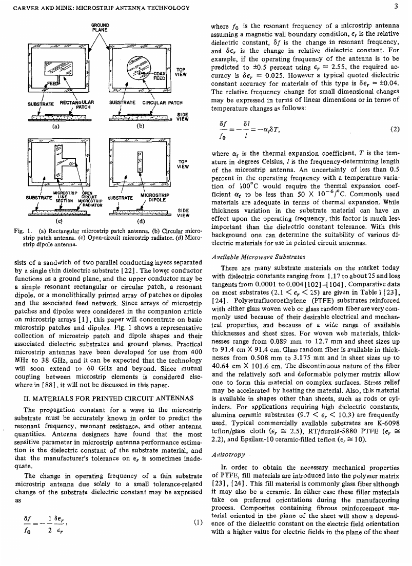
ature as shown in Fig. 2. For this material the average change
in dielectric constant over
to
to decrease with increasing temper-
is an uncertainty associated with
the temperature range -75'C
Because of fringing fields
the microwave region,
is about C ~ E = 96 ppm/'C. An abrupt transition
+100'C
change of about 6 e = 0.01 1, which occurs at a temperature
2OoC, is characteristic of PTFE-based
between zero and
materials. The exact temperature at which this
change occurs
is a function of the rate at which the temperature is changing.
Over the temperature range of -75'C
to 100°C the relative
change in operating frequencies is about 0.8 percent due to
changes
the change of dielectric
to com-
in linear dimensions due
pensate the effect
constant. Com-
bining (1) and (2) one obtains
constant. It turns out that
to thermal expansion tend
of a changing dielectric
range from -75'C
Over the temperature
net change of resonant frequency
with proper selection
of materials,
eliminate temperature effects on the resonant frequency
a microstrip patch antenna.
is 0.03 percent. Thus,
it is possible to almost
of
to 100' a typical
of PTFE-based
�
CARVER
t
t
2
.
-800
4
0
- 4 0 0
1
i
~
800
I
~
120-
'
~
'
"
0"
1
TEMPERATURE PC1
~
40-
Fig. 2. Dependence of dielectric constant on temperature for poly-
tetrafluoroethylene (PTFE) substrates. After Nowicki [23].
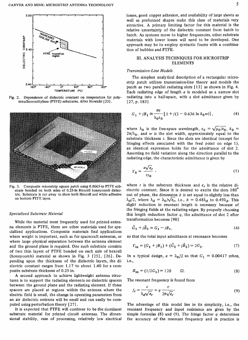
Fig. 3. Composite microstrip square patch using 0.0065-in FTFE sub-
strate bonded on both sides of 0.25-in Hexcell honeycomb dielec-
tric. Substrate is cut away to show both Hexcell and white adhesive
on bottom F'TFE layer.
Specialized Substrate Material
While the material most frequently used for printed anten-
used for spe-
na elements is PTFE, there are other materials
cialized applications. Composite materials find applications
where weight is important, such as for spacecraft antennas, or
where large physical separation between the antenna element
and the ground plane
is required. One such substrate consists
of two thin layers of PTFE bonded
(honeycomb) material
pending upon
electric constant ranges from
posite substrate thickness of 0.25 in.
on each side of hexcell
as shown in Fig. 3 [251, [261. De-
the di-
the thickness of the dielectric layers,
1 .I 7 to about 1.40 for a com-
A second approach
to achieve lightweight antenna struc-
tures is to support the radiating elements on dielectric spacers
between the ground plane and the radiating element. If these
spacers are placed
electric field is small, the change in operating parameters from
an air dielectric antenna will be small and can easily be com-
puted using perturbation theory [ 271.
the antenna where the
at regions within
It is expected that PTFE will continue to be the dominant
substrate material for printed circuit antennas. The dimen-
sional stability,
ease of processing, relatively low electrical
5
losses, good copper adhesion, and availability of large sheets as
class of materials very
well as preformed shapes make this
attractive. A primary limiting factor for this material
is the
relative uncertainty of the dielectric constant from batch
to
batch. As systems move to higher frequencies, other substrate
will need to be developed. One
materials with lower losses
approach may be to employ syntactic foams with a combina-
tion of bubbles and PTFE.
111. ANALYSIS TECHNIQUES FOR MICROSTRIP
ELEMENTS
Transmission-Line Models
The simplest analytical description of a rectangular micro-
strip patch utilizes transmission-line theory and models the
l
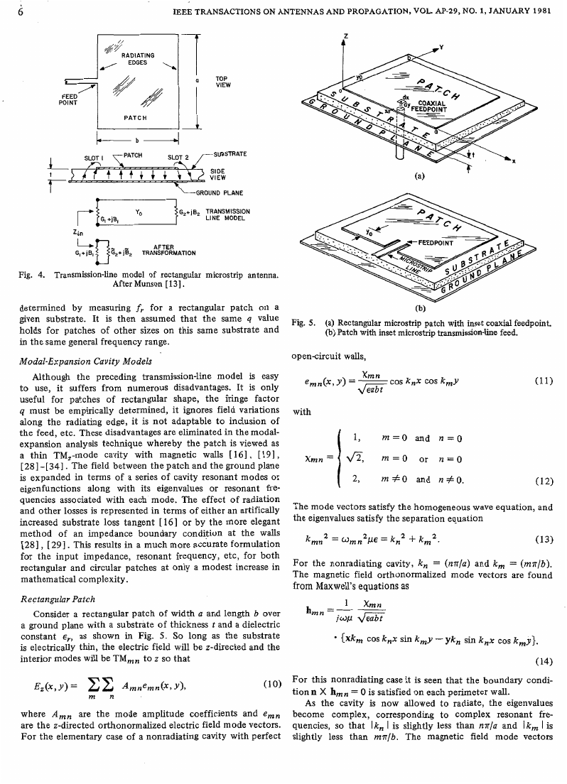
patch as two parallel radiating slots
Each radiating edge of length
radiating into a
[27, p. 183 1
a is modeled as a narrow slot
half-space, with a
[ 131 as shown in Fig. 4.
slot admittance given by
where ho is the free-space wavelength, zo = a, ko =
t. Since the slots are identical (except for
2a/ho, and w is the slot width, approximately equal to the
substrate thickness
fringing effects associated with
an identical expression holds for the admittance
Assuming no field variation along the direction parallel to the
radiating edge, the characteristic admittance is given by
the feed point on
edge l),
of slot 2.
where t is the substrate thickness and
E, is the relative di-
electric constant. Since it is desired to excite the slots 180'
out of phase, the dimension b is set equal to slightly less than
&/2, where & = hot&,
i.e., b = 0.48hd to 0.49hd. This
of
slight reduction in resonant length
the fringing fields at the radiating edges. By properly choosing
q , the admittance of slot 2 after
this length reduction factor
transformation becomes [ 901
is necessary because
z2 1- j i 2 = GI - j B 1 ,
( 6)
so that the total input admittance at resonance becomes
ri, = (C, + j B , ) + (Gz + j&) = 2G1.
typical design, a = X0/2 so that G1 = 0.00417 mhos,
(7)
In a
i.e.,
R h = (1/2G,) = 120 a.
The resonant frequency is found from
C
f y = - = q - .
M
r
C
2 b G r
The advantage of this model
i.e., the
resonant frequency and
given by the
simple formulas (8) and (9). The fringe factor q determines
in practice is
the accuracy
of the resonant frequency and
lies in its simplicity,
input resistance are
�
6
IEEE TRANSACTIONS ON ANTENNAS AND PROPAGATION, VOL. AP-29, NO. 1, JANUARY 1981
I
47’
I/
”
RADIATING
EDGES -4
7
TOP
VIEW
i
Fig. 5.
(a) Rectangular microstrip patch with inset coaxial feedpoint.
(b) Patch with inset microstrip transmission-line feed.
(b)
Zin
g,+ji,
AFTER
TRANSFORMATION
Fig. 4. Transmission-line model of
rectangular microstrip antenna.
After Munson [ 131.
determined by measuring f, for a rectangular patch on a
given substrate. It
holds for patches of other sizes on this same substrate and
in the same general frequency range.
is then assumed that the
same q value
&iodal-Expansion Cavity Models
open-circuit walls,
of rectangular shape,
Although the preceding transmission-line model
is easy
to use, it suffers from numerous disadvantages. It
is only
useful for patches
the fringe factor
q must be empirically determined, it ignores field variations
along the radiating edge, it is not adaptable to inclusion of
the feed, etc. These disadvantages are eliminated in the modal-
expansion analysis technique whereby the patch is viewed as
a thin TM,-mode cavity with magnetic
walls [ 161. [ 191,
[28] -[34]. The field between the patch and the ground plane
is expanded in terms of a series of cavity resonant modes or
eigenfunctions along with its eigenvalues or resonant
fre-
quencies associated with each mode. The effect of radiation
and other losses is represented in terms of either an artifically
[ 161 or by the more elegant
increased substrate loss tangent
method of an impedance boundary condition at the
walls
[28], [ 291. This results in a much more accurate formulation
for the input
etc, for both
rectangular and circular patches at only a modest increase in
mathematical complexity.
impedance, resonant frequency,
Rectangular Patch
Consider a rectangular patch of width a and length b over
a ground plane with a substrate of thickness f and a dielectric
constant E,, as shown in Fig. 5. So long as
the substrate
is electrically thin, the electric field will be z-directed and the
interior modes will be TM,,
to z so that
m
n
are the mode amplitude coefficients and
where A,,
are the z-directed orthonormalized electric field mode vectors.
For the elementary case of a nonradiating cavity with perfect
e,,
with
1,
m=O and n = O
fi,
2,
m =
or n = ~
~
m f O and n Z 0 .
(12)
The mode vectors satisfy the homogeneous wave equation, and
the eigenvalues satisfy the separation equation
kmn2 = u m n 2 p f = kn2 f k m 2 .
(13)
k , = (n.rr/a) and k , = (mn/b).
For the nonradiating cavity,
The magnetic field orthonormalized mode vectors are found
from Maxwell’s equations as
h,, =- - 1
Xmn
j u p &iE
*
COS knx sin kmy - ykn sin knx COS k m y } .
(14)
For this nonradiating case it is seen that the boundary condi-
tion n X hmn = 0 is satisfied on each perimeter wall.
As the cavity is now allowed to radiate, the
eigenvalues
become complex, corresponding to complex resonant
fre-
quencies, so that I k, I is slightly less than RK/a and lk, I is
slightly less than mx/b. The magnetic
field mode vectors
�
CARVER AND MINK: MICROSTRIP ANTENNA TECHNOLOGY
hmn no longer have a zero tangential component
cavity sidewalls. However
that the electric
given by (1 1).
field mode vectors are
a perturbational solution shows
still very accurately
Consider now
the effect of a z-directed current probe
Zo
of small rectangular cross section (d,dy) at (xo, y o ) as shown
in Fig. 5(a). The coefficients of each electric mode vector are
found from [ 271 :
\\/.I em,, * dv,
?zn
A m n =
k2 - k m n 2
which then
reduces
to
A m , = il, fi
k2
2 Gmn COS kmY0 coskrt~o
on the Therefore the input impedance
2, = 5 = -jZokr
x 9 m n 2 ( X o , Y O )
is
m
m
G m n .
10
m=o n=o k2 - kmn
7
( 2 2 )
5 )
.~
The (0, 0) term with
koo = 0 is the static capacitance
0) term represents the dominant
.
term with a shunt resistance to represent loss in the sub-
strate. The (1,
RF mode
transmission-line mode discussed in
and is identical to the
is
the previous section; for this mode,
cos (nylb) variation
no field variation
and
in the y direction. This mode is equivalent to a parallel R-L-C
network
where
losses. If the patch is square or nearly so, the (0, 1) mode can
also be excited
modes have negligible losses and sum
L .
All the higher order
to form a net inductance
as a degenerate mode.
(1 1 ) shows that there
the x direction
R represents
copper
radiation,
and
substrate,
a
in
Fig. 6(a) shows
a general network representation of the
(l6) input
impedance, and
Fig. 6(b) shows a network model
over a narrow band about an isolated
TMlo mode, where
the net series inductance is LT. The feed probe diameter
as
expressed by the factor G,,
is the major factor in determin-
ing L T , since it governs the convergence of the series. Equation
( 2 2 ) can be written as
where
Gmn =
sin (nndX/2a) sin (mndy/2b)
m?rdy/2b
nndX/2a
(17)
In (18) ij,, is the complex resonant frequency of the mnth
mode as found from (13). The relation (1 5 ) for the coefficients
is based on the orthogonality of the mode vectors; although
the introduction of the radiation condition means
that these
mode vectors are no longer orthogonal in the strict sense, for
electrically thin substrates the error due to this assumption
is negligible. The factor G,,
feed; for coaxial feeds
is set equal
d,d,
probe. For patches
yo = 0, set d , = 0 and use d , as the feed line width as a zero-
order approximation ignoring junction capacitance effects.
to the effective cross-section area
fed by a microstrip transmission line at
d, = d , and the cross-section area
accounts for the width
of the
of the
Substituting (16) into (10) we obtain
with Cdc being the dc patch capacitance ( ~ ~ b l t ) , Q the quality
factor for the TMlo mode, and w10 the radian frequency at
both w10 and Q
resonance. A simple means for determining
will be given in a subsequent paragraph. The
series inductive
reactance is given by
m n f O O
Xmn
9 m n =-
fi cos k,x cos kmy
The voltage at the feed is now computed as
v, =-fEz(Xo,Yo)
which shows that the
substrate thickness.
series reactance is proportional to the
The next problem is to find the complex eigenvalues kmn.
also the
Except near the TMlo mode resonant frequency (or
TMol resonant frequency for nearly square patches), kmn2
(mn/b)' -I- (n ?r/a)'. The complex eigenvalue
kl may be
found by either lumping all the losses into an effective
electric loss tangent [ 3 2 ] , or by incorporating the
into the conductance
of impedance-type boundary conditions
to a complex transcendental eigenvalue equation
di-
losses
of the radiating walls and imposition
[28], which leads
[ 2 9 ] which
�
8
IEEE TRANSACTIONS ON ANTENNAS AND PROPAGATION, VOL. AP-29, NO. 1, JANUARY 1.981
1
where
(Wo/b).
(33)
clo = (1 /2)cdc COS-2
In addition to radiation losses, the cavity also sustains losses
through the external surface wave (caused by the presence of
the substrate) as well as heat losses associated with the copper
(and adhesive fiim used to bond to the substrate) and the sub-
strate itself; for thin substrates, these
resonance in comparison to the
shown that the loss conductance referred to the input voltage
is given by
radiation loss. It may be
losses are small
at
where Rs = d
The substrate loss conductance is given by
a
is the wave resistance of the conductor.
Gdi = WC10 tan 6 (IT)
(35)
where tan 6 is the substrate loss tangent (typically 0.001 or
less). The total Q for thin substrates is therefore given by
W W
Q =- =
'lo w -'
Gin
TMo QRo0
I
I
(a)
Fig. 6.
(a) General network model representing microstrip antenna.
0) Network model over narrowband about
After Richards et al. [ 321.
isolated T M ~ o mode.
holds for thin substrates:
tan klob =
2kl O Q 1 0
k1o2 - a102
where
Pin
with Y , being the admittance of the radiating walls at y = 0
and y = b. A simple iterative algorithm has been developed
[29] for Tiding the complex eigenvalue, i.e.,
where
with A0 = 0 as a seed value.
Equation (30) is derived from
(27) with tan
k l o b expanded in the Test two terms of a
Taylor series about T . By using (27), klo is found as a com-
plex pole whose real part is typically from 96 to 98 percent of
(rib), and whose imaginary part is positive and proportional
This is equivalent to
to the
fringing factor q. The radiation
rigorously solving
quality factor is then found for thin substrates by [291
power lost through radiation.
for the
from which the radiation resistance at resonance (referred
the input) is found by
to
where Gin is the input conductance given by
In a practical design for an edge-fed patch, the input resistance
ranges from 100-200 R; this value can be reduced by insetting
the feed point for either coaxial inputs [ 191 or microstripline
inputs [351 by noting through (32) and (33) that the
radia-
tion resistance varies as cos2(Tyo/b). The antenna efficiency is '
given by
77=:
Grad
Gin
and ranges typically from 95 to 99 percent, i.e., from 0.2 to
0.05 dB.
Wall Admittance of Rectangular Patch
Radiated and reactively stored power in
the region ex-
cavity is represented as the wall admit-
in (28). No rigorous solutions for the
terior to the patch
tance Y,v, as used
wall admittance of a microstrip patch as yet have been found,
although several approximate solutions have been suggested,
including the admittance of a slot in a ground plane
a parallel-plate
[ 191, the
line [37], [981, [99],
rectangular microstrip patch
[38]. None of these analogous
geometries is completely satisfactory, and a solution with full
on the
generality awaits
Wiener-Hopf method [39], [40]. In the absence of a rigorous
solution, a
reasonable approach is to assume that the wall
fringe admittance of a microstrip transmission
and a Green's function for a long
current work in progress based
TEM waveguide radiating
[ 361,
half-space
into a
�
CARVER AND MINK: MICROSTRIP ANTENNA TECHNOLOGY
9
angle of incidence, which
on the exterior grounded substrate.
that the wall admittance is
which can propagate
Importantly, this analysis shows
a function of both frequency and
then shows that Y , cannot be rigorously represented by
the
(39) or (40) which assume normal
approximate expressions
Y , will depend
incidence. We may therefore anticipate that
on both dimensions a and b. Carver [ 291, by near-field prob-
ing of the fields near the wall, has shown empirically that the
wall admittance expressions
modified by multiplying Y , by an aspect ratio factor F,,(a/b)
given by
F ~ ( Q / ~ ) = 0.7747 + 0.5977 (a/b - I ) - 0.1638 (a/b - 112,
(44)
and (43) may be
(39), (40),
to better agreement of the predicted resonant
and S-band than by assuming that
fre-
to its validity is unknown; clearly more work
which leads
resistance and resonant frequency versus aspect ratio with
measured results at L-band
F,, = 1. Nonetheless, (44) is empirical, and
quency limit
in the numerical evaluation of the Wiener-Hopf solution is.
needed, perhaps reducing this to
as given in (44).
Radiation Pattern of Rectangular Patch
curve-fit polynomials such
the upper
The far-field radiation pattern of a rectangular microstrip
is broad in both the
in the TMlo mode
E
ground
by modeling the radiator as either
of length a, sep-
patch operating
and H planes. The pattern of a patch over a large
plane may be calculated
two parallel uniform magnetic line sources
arated by distance
current sources as suggested in Fig. 7. The effect of the ground
an
plane and substrate
electrical distance k t . If the slot voltage across either radiating
edge is taken as VO, the calculated fields are
b [96], or as two equivalent electric
is handled by imaging
the slot at
J
ko - sin 0 sin q5
a
2
conductance is that of a wave normally incident on a pard-
lel-plate TEM waveguide slot radiating into a half-space [271;
for electrically small slot widths,
length is given by n/(376ho) mho/m. If it is further assumed
is excited, then the wave
that only the dominant TMlo mode
the field
is normally incident on the radiating edges with
intensity being uniform across both
this
case the total wall conductance is given by
the conductance per unit
of these edges. In
G, = (n/376)(a/b)
(7Jr).
(39)
The wall susceptance may be approximated from Hammer-
stad’s formula for
circuit [ 371 and assumes the form
the capacitance of an open microstrip
B , = 0.01668 (AZ/t)(a/x,)e,
where
(u),
(40)
a - + 0.262
t
- + 0.813
a
t
1 +l&]-”’
and E, is an effective dielectric constant given by [41]
ee=-+- e,+ 1
2
2
E,--- 1
so that the TMlo
edges is
lumped wall admittance of the radiating
Y , = G, i- jB,.
(43)
It should be noted that the susceptance given by (40) is based
on Hammerstad’s nondispersive
and disagrees with the susceptance given in (4) which is based
is rigorously
on a dynamic capacitance. Neither formula
correct for the microstrip antenna, and better relations await
theoretical work in progress.
static capacitance relation
It will be shown in a subsequent section that (39) and (40)
lead to a prediction of resonant input resistance and resonant
frequency which is in good agreement with measured results
for the aspect ratios 1 < a/b < 2; for larger aspect ratios, the
assumption of a uniform field and normal incidence on the ra-
diating edges is no longer very good, so that (39) and (40) are in-
sufficiently accurate. The advantage to this impedance bound-
ary condition method
field
through Y , is that it explicitly provides (through
the eigen-
value equation (27)) for improved solutions
problem, when these are published in future literature.
of representing the exterior
to the exterior
It should be mentioned that the mode vectors of (1 1) may
be viewed as spatial harmonics resulting from
the resonance
of quasi-TEM plane waves launched from the feed which, by
zig-zagging off the cavity parameter wall, travel a total distance
the walls so as to produce con-
and experience phase shifts at
structive interference. An analysis of this resonance condition
as a function of the patch aspect ratio a/b has been provided
by Chang and Kuester [ 421 , who have shown that an optimum
in the sense of low-Q opera-
range for the aspect ratio exists
tion. The Wiener-Hopf technique was used to obtain the wall
reflection coefficient
in p M -
strate thickness, and dielectric constant)
ciple then be used
re-
flection coefficient involves two infinite integrals, the evalua-
tion of which reveals both LSE and LSM surface-wave modes
(as a function of incidence angle, sub-
to obtain the wall admittance. The
which may
�



 2023年江西萍乡中考道德与法治真题及答案.doc
 2012年重庆南川中考生物真题及答案.doc
 2013年江西师范大学地理学综合及文艺理论基础考研真题.doc
 2020年四川甘孜小升初语文真题及答案I卷.doc
 2020年注册岩土工程师专业基础考试真题及答案.doc
 2023-2024学年福建省厦门市九年级上学期数学月考试题及答案.doc
 2021-2022学年辽宁省沈阳市大东区九年级上学期语文期末试题及答案.doc
 2022-2023学年北京东城区初三第一学期物理期末试卷及答案.doc
 2018上半年江西教师资格初中地理学科知识与教学能力真题及答案.doc
 2012年河北国家公务员申论考试真题及答案-省级.doc
 2020-2021学年江苏省扬州市江都区邵樊片九年级上学期数学第一次质量检测试题及答案.doc
 2022下半年黑龙江教师资格证中学综合素质真题及答案.doc