www.ti.com.cn
LDC1000 电电感感数数字字转转换换器器
查查询询样样品品: LDC1000
LDC1000
ZHCSBM0 –SEPTEMBER 2013
说说明明
电感感测是一种遥控的、短程感测技术,此项技术能够
在灰尘、污垢、油和潮湿环境中实现导体目标的低成
本、高分辨率感测,这使得它在恶劣环境中非常可靠。
通过使用可在印刷电路板 (PCB) 上被创建为一个感测
元件的线圈,LDC1000 可实现超低成本系统解决方
案。
电感感测技术可实现线性/角位置、位移、运动、压
缩、振动、金属成分以及市面上包括汽车、消费类、计
算机、工业用、医疗用和通信应用在内的很多其它应用
的高精度测量。 电感感测以低于其它竞争对手解决方
案的成本提供更佳的性能和可靠性。
LDC1000 是世界上第一个电感数字转换器,从而在一
个低功耗、小封装尺寸解决方案内提供电感感测的优
势。 此产品采用一个小外形尺寸无引线 (SON)-16 封
装,并且提供了几种运行模式。 一个串行外设接口
(SPI) 简化了到微控制器 (MCU) 的连接。
1特特性性
• 无无磁磁体体操操作作
• 亚亚微微米米高高精精度度
• 可可调调感感测测范范围围((通通过过线线圈圈设设计计实实现现))
• 更更低低的的系系统统成成本本
• 远远程程传传感感器器放放置置((从从恶恶劣劣环环境境中中将将 LDC 去去耦耦合合))
• 高高耐耐久久性性((借借助助于于遥遥控控操操作作))
• 对对于于环环境境干干扰扰的的不不敏敏感感性性((诸诸如如污污垢垢、、灰灰尘尘、、水水、、
油油))
• 电电源源电电压压,,模模拟拟::4.75V 至至 5.25V
• 电电源源电电压压,,IO::1.8V 至至 5.25V
• 电电源源电电流流((无无 LC 谐谐振振回回路路))::1.7mA
• Rp 分分辨辨率率::16 位位
• L 分分辨辨率率::24 位位
• LC 频频率率范范围围::5kHz 至至 5MHz
应应用用范范围围
• 电电传传线线控控系系统统
• 轮轮齿齿计计数数
• 流流量量计计
• 按按钮钮开开关关
• 笔笔记记本本电电脑脑
• 游游戏戏控控制制器器
• 多多功功能能打打印印机机
• 数数码码照照相相机机
• 医医疗疗设设备备
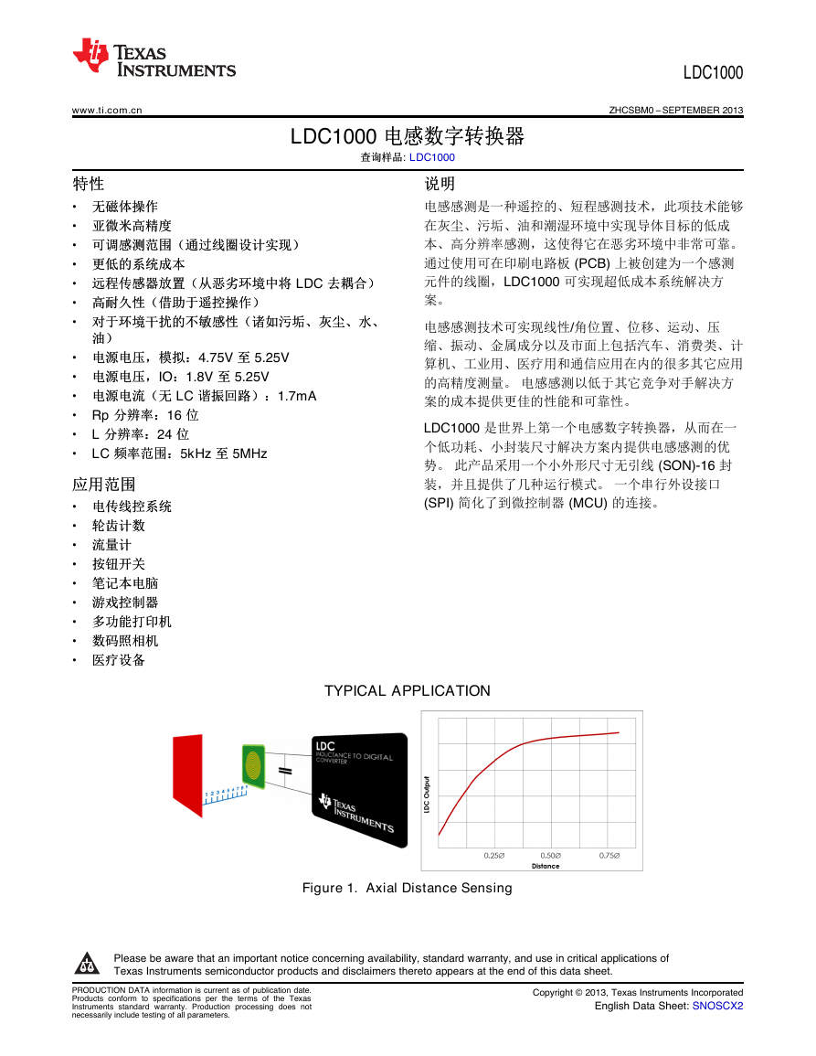
TYPICAL APPLICATION
Figure 1. Axial Distance Sensing
1
Please be aware that an important notice concerning availability, standard warranty, and use in critical applications of
Texas Instruments semiconductor products and disclaimers thereto appears at the end of this data sheet.
PRODUCTION DATA information is current as of publication date.
Products conform to specifications per the terms of
the Texas
Instruments standard warranty. Production processing does not
necessarily include testing of all parameters.
Copyright © 2013, Texas Instruments Incorporated
English Data Sheet: SNOSCX2
�
LDC1000
ZHCSBM0 –SEPTEMBER 2013
www.ti.com.cn
This integrated circuit can be damaged by ESD. Texas Instruments recommends that all
appropriate precautions. Failure to observe proper handling and installation procedures can cause damage.
ESD damage can range from subtle performance degradation to complete device failure. Precision integrated circuits may be more
susceptible to damage because very small parametric changes could cause the device not to meet its published specifications.
integrated circuits be handled with
BLOCK DIAGRAM
Figure 2. LDC1000 Block Diagram
TYPICAL APPLICATION SCHEMATIC
Figure 3. Typical Application Schematic
2
Copyright © 2013, Texas Instruments Incorporated
MCULDOLDC10005V5VDGNDDGNDAGNDSensorVIODGNDVIOVDDVIOCLDOSDISDOSCLKCSBINTBTBCLKDGNDMOSIMISOSCLKGPIOINT/GPIOTimer/Aux CLKDAPGNDCFBCFAINBINA4-WireSerialInterfaceINAINBSCLKSDISDOCSINTBVDDCFACFBPowerGNDVIODGNDCLDORsLCFrequency CounterTBCLK/XINXOUTThresholdDetectorFrequency Counter Data RegisterProximity DataRegisterLDC�
www.ti.com.cn
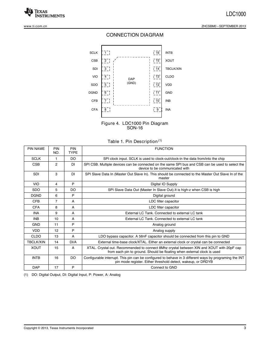
CONNECTION DIAGRAM
LDC1000
ZHCSBM0 –SEPTEMBER 2013
Figure 4. LDC1000 Pin Diagram
SON-16
Table 1. Pin Description(1)
FUNCTION
SPI clock input. SCLK is used to clock-out/clock-in the data from/into the chip
SPI CSB. Multiple devices can be connected on the same SPI bus and CSB can be used to select the
device to be communicated with
SPI Slave Data In (Master Out Slave In). This should be connected to the Master Out Slave In of the
master
SPI Slave Data Out (Master In Slave Out).It is high-z when CSB is high
Digital IO Supply
Digital ground
LDC filter capacitor
LDC filter capacitor
External LC Tank. Connected to external LC tank
External LC Tank. Connected to external LC tank
Analog ground
Analog supply
LDO bypass capacitor. A 56nF capacitor should be connected from this pin to GND
External time-base clock/XTAL. Either an external clock or crystal can be connected
XTAL. Crystal out. Recommended to connect 8Mhz crystal between XIN and XOUT with 20pF cap
from each pin to ground. Should be floating when external clock is used
Configurable interrupt. This pin can be configured to behave in 3 different ways by programing the INT
pin mode register. Either threshold detect, wakeup, or DRDYB
Connect to GND
PIN NAME
SCLK
CSB
SDI
VIO
SDO
DGND
CFB
CFA
INA
INB
GND
VDD
CLDO
TBCLK/XIN
XOUT
INTB
DAP
PIN
NO.
1
2
PIN
TYPE
DO
DI
3
4
5
6
7
8
9
10
11
12
13
14
15
16
17
DI
P
DO
P
A
A
A
A
P
P
A
DI/A
A
DO
P
(1) DO: Digital Output, DI: Digital Input, P: Power, A: Analog
Copyright © 2013, Texas Instruments Incorporated
3
116765432101112131415DAP(GND)SCLKSDODGNDCFBVDDCLDOXOUTINBGNDTBCLK/XININTB89CSBSDIVIOCFAINA�
LDC1000
ZHCSBM0 –SEPTEMBER 2013
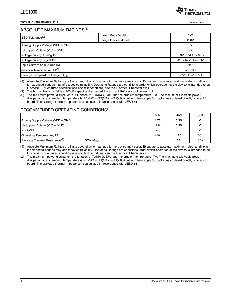
ABSOLUTE MAXIMUM RATINGS(1)
ESD Tolerance(2)
Human Body Model
Charge Device Model
www.ti.com.cn
1kV
250V
6V
6V
Analog Supply Voltage (VDD – GND)
IO Supply Voltage (VIO – GND)
Voltage on any Analog Pin
Voltage on any Digital Pin
Input Current on INA and INB
Junction Temperature, TJ(3)
Storage Temperature Range , Tstg
(1) Absolute Maximum Ratings are limits beyond which damage to the device may occur. Exposure to absolute-maximum-rated conditions
for extended periods may affect device reliability. Operating Ratings are conditions under which operation of the device is intended to be
functional. For ensured specifications and test conditions, see the Electrical Characteristics.
-0.3V to VDD + 0.3V
-0.3V to VIO + 0.3V
8mA
+150°C
-65°C to +150°C
(2) The human body model is a 100pF capacitor discharged through a 1.5kΩ resistor into each pin.
(3) The maximum power dissipation is a function of TJ(MAX), θJA, and the ambient temperature, TA. The maximum allowable power
dissipation at any ambient temperature is PDMAX = (TJ(MAX) - TA)/ θJA. All numbers apply for packages soldered directly onto a PC
board. The package thermal impedance is calculated in accordance with JESD 51-7.
RECOMMENDED OPERATING CONDITIONS(1)
Analog Supply Voltage (VDD – GND)
IO Supply Voltage (VIO – GND)
VDD-VIO
Operating Temperature, TA
Package Thermal Resistance(2)
SON (θJA)
MIN
4.75
1.8
>=0
-40
MAX
5.25
5.25
125
28
UNIT
V
V
V
°C
°C/W
(1) Absolute Maximum Ratings are limits beyond which damage to the device may occur. Exposure to absolute-maximum-rated conditions
for extended periods may affect device reliability. Operating Ratings are conditions under which operation of the device is intended to be
functional. For ensured specifications and test conditions, see the Electrical Characteristics.
(2) The maximum power dissipation is a function of TJ(MAX), θJA, and the ambient temperature, TA. The maximum allowable power
dissipation at any ambient temperature is PDMAX = (TJ(MAX) - TA)/ θJA. All numbers apply for packages soldered directly onto a PC
board. The package thermal impedance is calculated in accordance with JESD 51-7.
4
Copyright © 2013, Texas Instruments Incorporated
�
www.ti.com.cn
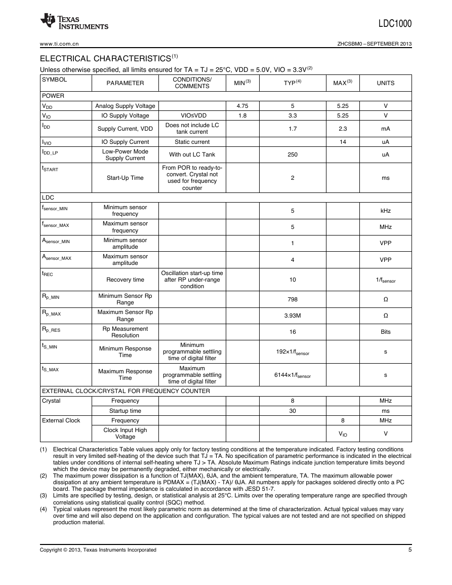
ELECTRICAL CHARACTERISTICS(1)
Unless otherwise specified, all limits ensured for TA = TJ = 25°C, VDD = 5.0V, VIO = 3.3V(2)
SYMBOL
MIN(3)
TYP(4)
PARAMETER
CONDITIONS/
COMMENTS
POWER
VDD
VIO
IDD
IVIO
IDD_LP
tSTART
LDC
fsensor_MIN
fsensor_MAX
Asensor_MIN
Asensor_MAX
tREC
Rp_MIN
Rp_MAX
Rp_RES
tS_MIN
tS_MAX
Analog Supply Voltage
IO Supply Voltage
Supply Current, VDD
IO Supply Current
Low-Power Mode
Supply Current
Start-Up Time
Minimum sensor
frequency
Maximum sensor
frequency
Minimum sensor
amplitude
Maximum sensor
amplitude
Recovery time
Minimum Sensor Rp
Range
Maximum Sensor Rp
Range
Rp Measurement
Resolution
Minimum Response
Time
Maximum Response
Time
4.75
1.8
VIO≤VDD
Does not include LC
tank current
Static current
With out LC Tank
From POR to ready-to-
convert. Crystal not
used for frequency
counter
Oscillation start-up time
after RP under-range
condition
Minimum
programmable settling
time of digital filter
Maximum
programmable settling
time of digital filter
EXTERNAL CLOCK/CRYSTAL FOR FREQUENCY COUNTER
Crystal
External Clock
Frequency
Startup time
Frequency
Clock Input High
Voltage
5
3.3
1.7
250
2
5
5
1
4
10
798
3.93M
16
192×1/fsensor
6144×1/fsensor
8
30
LDC1000
ZHCSBM0 –SEPTEMBER 2013
MAX(3)
UNITS
5.25
5.25
2.3
14
8
VIO
V
V
mA
uA
uA
ms
kHz
MHz
VPP
VPP
1/fsensor
Ω
Ω
Bits
s
s
MHz
ms
MHz
V
(1) Electrical Characteristics Table values apply only for factory testing conditions at the temperature indicated. Factory testing conditions
result in very limited self-heating of the device such that TJ = TA. No specification of parametric performance is indicated in the electrical
tables under conditions of internal self-heating where TJ > TA. Absolute Maximum Ratings indicate junction temperature limits beyond
which the device may be permanently degraded, either mechanically or electrically.
(2) The maximum power dissipation is a function of TJ(MAX), θJA, and the ambient temperature, TA. The maximum allowable power
dissipation at any ambient temperature is PDMAX = (TJ(MAX) - TA)/ θJA. All numbers apply for packages soldered directly onto a PC
board. The package thermal impedance is calculated in accordance with JESD 51-7.
(3) Limits are specified by testing, design, or statistical analysis at 25°C. Limits over the operating temperature range are specified through
correlations using statistical quality control (SQC) method.
(4) Typical values represent the most likely parametric norm as determined at the time of characterization. Actual typical values may vary
over time and will also depend on the application and configuration. The typical values are not tested and are not specified on shipped
production material.
Copyright © 2013, Texas Instruments Incorporated
5
�
LDC1000
ZHCSBM0 –SEPTEMBER 2013
ELECTRICAL CHARACTERISTICS(1) (continued)
Unless otherwise specified, all limits ensured for TA = TJ = 25°C, VDD = 5.0V, VIO = 3.3V(2)
SYMBOL
PARAMETER
CONDITIONS/
COMMENTS
MIN(3)
TYP(4)
DIGITAL I/O CHARACTERISTICS
VIH
VIL
VOH
Logic "1" Input Voltage
Logic "0" Input Voltage
Logic "1" Output
Voltage
VOL
IIOHL
Logic "0" Output
Voltage
Digital IO Leakage
Current
ISOURCE=400uA
ISINK=400uA
0.8×VIO
-500
VIO-0.3
www.ti.com.cn
MAX(3)
UNITS
0.2×VIO
0.3
500
V
V
V
V
nA
6
Copyright © 2013, Texas Instruments Incorporated
�
www.ti.com.cn
TIMING DIAGRAMS
LDC1000
ZHCSBM0 –SEPTEMBER 2013
Unless otherwise noted, all limits specified at TA = 25°C, VDD=5.0, VIO=3.3, 10pF capacitive load in parallel with
a 10kΩ load on SDO. Specified by design; not production tested.
Figure 5. Write Timing Diagram
Table 2.
PARAMETER
CONDITIONS
MIN
TYP
FSCLK
tPH
tPL
tSU
tH
Serial Clock Frequency
SCLK Pulse Width High
SCLK Pulse Width Low
SDI Setup Time
SDI Hold Time
FSCLK=4Mhz
FSCLK=4Mhz
0.4/Fsclk
0.4/Fsclk
10
10
MAX
4
Figure 6. Read Timing Diagram
PARAMETER
CONDITIONS
MIN
TYP
tODZ
tOZD
tOD
tCSS
tCSH
tIAG
tDRDYB
SDO Driven-to-Tristate
Time
SDO Tristate-to-Driven
Time
SDO Output Delay Time
CSB Setup Time
CSB Hold Time
Inter-Access Gap
Data ready pulse width
Measured at 10% / 90% point
Measured at 10% / 90% point
20
20
100
Data ready pulse at every 1/ODR if
no data is read
1/fsensor
MAX
20
20
20
UNIT
MHz
s
s
ns
ns
UNIT
ns
ns
ns
ns
ns
ns
s
Copyright © 2013, Texas Instruments Incorporated
7
SCLKSDIttCSHtttCSSt16th ClockSCLKxxxxxxttCSHtttCSStD7D1D01st Clock8th ClockttHttODtOZDSCLKSDIttPLtValid DataValid DatattPHtttSUtttHt16th Clock�
LDC1000
ZHCSBM0 –SEPTEMBER 2013
THEORY OF OPERATION
www.ti.com.cn
Inductive Sensing
An AC current flowing through a coil will generate an AC magnetic field. If a conductive material, such as a metal
target, is brought into the vicinity of the coil, this magnetic field will induce circulating currents (eddy currents) on
the surface of the target. These eddy currents are a function of the distance, size, and composition of the target.
These eddy currents then generate their own magnetic field, which opposes the original field generated by the
coil. This mechanism is best compared to a transformer, where the coil is the primary core and the eddy current
is the secondary core. The inductive coupling between both cores depends on distance and shape. Hence the
resistance and inductance of the secondary core (Eddy current), shows up as a distant dependent resistive and
inductive component on the primary side (coil). The figures below show a simplified circuit model.
Figure 7.
Inductor with a Metal Target
Eddy currents generated on the surface of the target can be modeled as a transformer as shown in Figure 8. The
coupling between the primary and secondary coils is a function of the distance and conductor’s characteristics. In
Figure 8,
the inductance Ls is the coil’s inductance, and Rs is the coil’s parasitic series resistance. The
inductance L(d), which is a function of distance d, is the coupled inductance of the metal target. Likewise, R(d) is
the parasitic resistance of the eddy currents.
Figure 8. Metal Target Modeled as L and R with Circulating Eddy Currents
8
Copyright © 2013, Texas Instruments Incorporated
Target Metal SurfaceConductance of MetalLs + L(d)Rs + R(d)Distance dEddy CurrentsMetal Targetd�



 2023年江西萍乡中考道德与法治真题及答案.doc
 2012年重庆南川中考生物真题及答案.doc
 2013年江西师范大学地理学综合及文艺理论基础考研真题.doc
 2020年四川甘孜小升初语文真题及答案I卷.doc
 2020年注册岩土工程师专业基础考试真题及答案.doc
 2023-2024学年福建省厦门市九年级上学期数学月考试题及答案.doc
 2021-2022学年辽宁省沈阳市大东区九年级上学期语文期末试题及答案.doc
 2022-2023学年北京东城区初三第一学期物理期末试卷及答案.doc
 2018上半年江西教师资格初中地理学科知识与教学能力真题及答案.doc
 2012年河北国家公务员申论考试真题及答案-省级.doc
 2020-2021学年江苏省扬州市江都区邵樊片九年级上学期数学第一次质量检测试题及答案.doc
 2022下半年黑龙江教师资格证中学综合素质真题及答案.doc