18-Port, 48-Lane, 240Gbps,
Gen2 RapidIO Switch
CPS-1848
Datasheet
Description
The CPS-1848 (80HCPS1848) is a RapidIO Specification (Rev. 2.1)
compliant Central Packet Switch whose functionality is central to
routing packets for distribution among DSPs, processors, FPGAs,
other switches, or any other RapidIO-based devices. It can also be
used in RapidIO backplane switching. The CPS-1848 supports Serial
RapidIO (S-RIO) packet switching (unicast, multicast, and an optional
broadcast) from any of its 18 input ports to any of its 18 output ports.
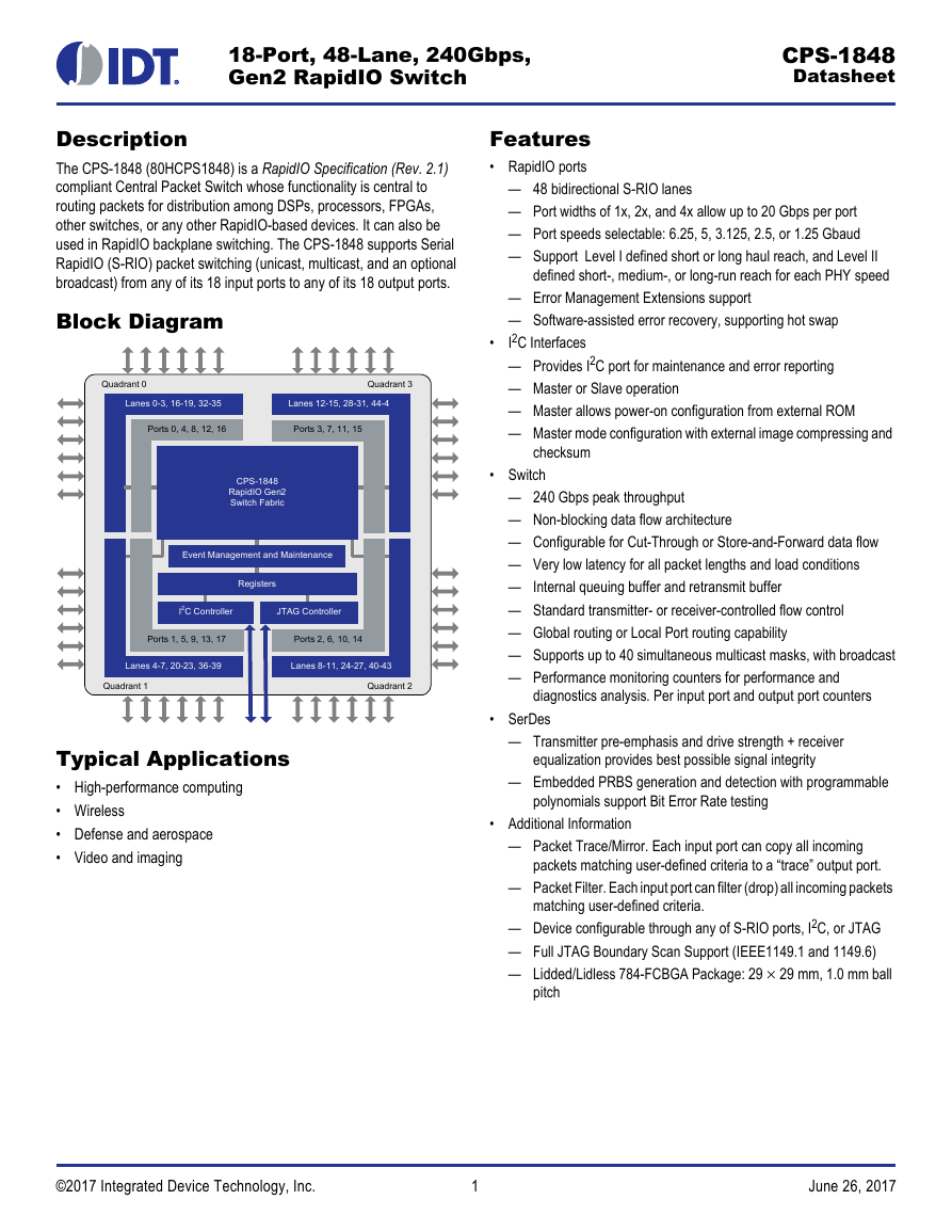
Block Diagram
Quadrant 0
Quadrant 3
Lanes 0-3, 16-19, 32-35
Lanes 12-15, 28-31, 44-47
Ports 0, 4, 8, 12, 16
Ports 3, 7, 11, 15
CPS-1848
RapidIO Gen2
Switch Fabric
Event Management and Maintenance
Registers
I2C Controller
JTAG Controller
Ports 1, 5, 9, 13, 17
Ports 2, 6, 10, 14
Lanes 4-7, 20-23, 36-39
Lanes 8-11, 24-27, 40-43
Quadrant 1
Quadrant 2
Typical Applications
• High-performance computing
• Wireless
• Defense and aerospace
• Video and imaging
Features
• RapidIO ports
— 48 bidirectional S-RIO lanes
— Port widths of 1x, 2x, and 4x allow up to 20 Gbps per port
— Port speeds selectable: 6.25, 5, 3.125, 2.5, or 1.25 Gbaud
— Support Level I defined short or long haul reach, and Level II
defined short-, medium-, or long-run reach for each PHY speed
— Error Management Extensions support
— Software-assisted error recovery, supporting hot swap
I2C Interfaces
— Provides I2C port for maintenance and error reporting
— Master or Slave operation
— Master allows power-on configuration from external ROM
— Master mode configuration with external image compressing and
checksum
•
• Switch
— 240 Gbps peak throughput
— Non-blocking data flow architecture
— Configurable for Cut-Through or Store-and-Forward data flow
— Very low latency for all packet lengths and load conditions
— Internal queuing buffer and retransmit buffer
— Standard transmitter- or receiver-controlled flow control
— Global routing or Local Port routing capability
— Supports up to 40 simultaneous multicast masks, with broadcast
— Performance monitoring counters for performance and
diagnostics analysis. Per input port and output port counters
• SerDes
— Transmitter pre-emphasis and drive strength + receiver
equalization provides best possible signal integrity
— Embedded PRBS generation and detection with programmable
polynomials support Bit Error Rate testing
• Additional Information
— Packet Trace/Mirror. Each input port can copy all incoming
packets matching user-defined criteria to a “trace” output port.
— Packet Filter. Each input port can filter (drop) all incoming packets
matching user-defined criteria.
— Device configurable through any of S-RIO ports, I2C, or JTAG
— Full JTAG Boundary Scan Support (IEEE1149.1 and 1149.6)
— Lidded/Lidless 784-FCBGA Package: 29 29 mm, 1.0 mm ball
pitch
©2017 Integrated Device Technology, Inc.
1
June 26, 2017
�
CPS-1848 Datasheet
3.
4.
Table of Contents
1. About This Document.................................................................................................................... 4
Introduction............................................................................................................................................................................................................ 4
Additional Resources............................................................................................................................................................................................. 4
Document Conventions and Definitions................................................................................................................................................................. 4
Revision History..................................................................................................................................................................................................... 4
2. Device Description ........................................................................................................................ 6
Specification Compliancy....................................................................................................................................................................................... 7
Functional Overview ..................................................................................................................... 7
Interface Overview........................................................................................................................ 8
S-RIO Ports ........................................................................................................................................................................................................... 8
I2C Bus.................................................................................................................................................................................................................. 8
JTAG TAP Port...................................................................................................................................................................................................... 8
Interrupt (IRQ_N)................................................................................................................................................................................................... 8
Reset (RST_N) ...................................................................................................................................................................................................... 8
Clock (REF_CLK_P/N) .......................................................................................................................................................................................... 8
Rext (REXT_N/P) .................................................................................................................................................................................................. 9
Speed Select (SPD[2:0])........................................................................................................................................................................................ 9
Quadrant Config (QCFG[7:0])................................................................................................................................................................................ 9
Frequency Select (FSEL[1:0]) ............................................................................................................................................................................... 9
Multicast (MCAST)................................................................................................................................................................................................. 9
5. Configuration Pins ....................................................................................................................... 10
Speed Select Pins SPD[2:0]................................................................................................................................................................................ 10
Quadrant Configuration Pins QCFG[7:0]............................................................................................................................................................. 10
6. Absolute Maximum Ratings ........................................................................................................ 14
7. Recommended Operating Conditions ......................................................................................... 15
8. AC Test Conditions...................................................................................................................... 16
9.
Power Consumption .................................................................................................................... 18
I2C Bus......................................................................................................................................... 19
10.
I2C Master Mode and Slave Mode....................................................................................................................................................................... 19
I2C Device Address ............................................................................................................................................................................................. 19
Signaling.............................................................................................................................................................................................................. 20
Read/Write Figures.............................................................................................................................................................................................. 21
I2C DC Electrical Specifications........................................................................................................................................................................... 23
I2C AC Electrical Specifications........................................................................................................................................................................... 24
I2C Timing Waveforms......................................................................................................................................................................................... 25
11.
Interrupt (IRQ_N) Electrical Specifications ................................................................................ 26
12. Configuration (Static) Pin Specification ..................................................................................... 27
13. S-RIO Ports .................................................................................................................................. 28
Overview.............................................................................................................................................................................................................. 28
Definition of Amplitude and Swing....................................................................................................................................................................... 29
1.25, 2.5, and 3.125 Gbaud LP-Serial Links........................................................................................................................................................ 30
Level I Electrical Specification ............................................................................................................................................................................. 30
5 and 6.25 Gbaud LP-Serial Links....................................................................................................................................................................... 37
Level II Electrical Specifications .......................................................................................................................................................................... 37
©2017 Integrated Device Technology, Inc.
2
June 26, 2017
�
CPS-1848 Datasheet
14. Reference Clock .......................................................................................................................... 47
Reference Clock Electrical Specifications ........................................................................................................................................................... 47
15. Reset (RST_N) Specification ....................................................................................................... 49
16. JTAG Interface ............................................................................................................................ 50
Description........................................................................................................................................................................................................... 50
IEEE 1149.1 (JTAG) and IEEE 1149.6 (AC Extest) Compliance ........................................................................................................................ 50
System Logic TAP Controller Overview............................................................................................................................................................... 50
Signal Definitions................................................................................................................................................................................................. 51
Test Data Register (DR) ...................................................................................................................................................................................... 52
Boundary Scan Registers.................................................................................................................................................................................... 52
Instruction Register (IR)....................................................................................................................................................................................... 55
EXTEST............................................................................................................................................................................................................... 56
Configuration Register Access (Revision A/B) .................................................................................................................................................... 58
Configuration Register Access (Revision C)........................................................................................................................................................ 60
JTAG DC Electrical Specifications....................................................................................................................................................................... 63
JTAG AC Electrical Specifications....................................................................................................................................................................... 64
JTAG Timing Waveforms..................................................................................................................................................................................... 65
17. Pinout and Pin Listing ................................................................................................................. 66
Pinout — Top View.............................................................................................................................................................................................. 66
Pin Listing ............................................................................................................................................................................................................ 67
18. Package Specifications .............................................................................................................. 77
Package Physical Specifications ......................................................................................................................................................................... 77
Package Outline Drawings .................................................................................................................................................................................. 78
Thermal Characteristics....................................................................................................................................................................................... 83
19. Ordering Information ................................................................................................................... 85
©2017 Integrated Device Technology, Inc.
3
June 26, 2017
�
CPS-1848 Datasheet
About This Document
1.
Introduction
The CPS-1848 Datasheet provides hardware information about the CPS-1848, such as electrical and packaging characteristics. It is intended for
hardware engineers who are designing system interconnect applications with the device.
Additional Resources
The CPS-1848 User Manual describes the functionality and configuration capabilities of the device. In addition, there are many other resources
available that support the CPS-1848. For more information, please contact IDT for support.
Document Conventions and Definitions
This document uses the following conventions and definitions:
•
To indicate signal states:
– Differential signals use the suffix “_P” to indicate the positive half of a differential pair.
– Differential signals use the suffix “_N” to indicate the negative half of a differential pair.
– Non-differential signals use the suffix “_N” to indicate an active-low state.
To define buses, the most significant bit (MSB) is on the left and least significant bit (LSB) is on the right. No leading zeros are included.
To represent numerical values, either decimal, binary, or hexadecimal formats are used. The binary format is as follows: 0bDDD, where “D”
represents either 0 or 1; the hexadecimal format is as follows: 0xDD, where “D” represents the hexadecimal digit(s); otherwise, it is decimal.
• Unless otherwise denoted, a byte refers to an 8-bit quantity; a word refers to a 32-bit quantity, and a double word refers to an 8-byte (64-bit)
•
•
quantity. This is in accordance with RapidIO convention.
• A bit is set when its value is 0b1. A bit is cleared when its value is 0b0.
• A read-only register, bit, or field is one that can be read but not modified.
This symbol indicates important configuration information or suggestions.
This symbol indicates procedures or operating levels that may result in misuse or damage to
the device.
Revision History
June 26, 2017
• Updated the Package Outline Drawings; no technical changes
• Updated the Ordering Information
April 4, 2016
• Added an R_X2 symbol to Table 20
• Updated the Package Physical Specifications
• Updated Heat Sink Requirement and Analysis
• Added HMH, HMG, and BLG part numbers to Ordering Information
June 12, 2013
• Updated the note associated with VDD3A (pin AD24)
June 8, 2012
• Changed the maximum 3.3V supply requirement to 3.47V in Table 6 and note 2 below the table
• Added two cautionary notes about lane reordering to Pin Listing
©2017 Integrated Device Technology, Inc.
4
June 26, 2017
�
CPS-1848 Datasheet
April 2, 2012
• Added JTAG configuration register access information for Revision C in Configuration Register Access (Revision C)
• Updated the JTAG version number for Revision C
• Added a BR FCBGA (Lidded) package option to Package Outline Drawings
• Added new thermal data for the BR FCBGA package to Thermal Characteristics
• Added BR FCBGA package information to Ordering Information
December 9, 2011
•
• Added an additional note to the power sequencing requirements
Loosened the Clock Input signal rise/fall minimum time specification
©2017 Integrated Device Technology, Inc.
5
June 26, 2017
�
CPS-1848 Datasheet
Device Description
2.
The CPS-1848 is a S-RIO-compliant performance-optimized switch. This device is ideally suited for intensive processing applications which
require a multiplicity of DSPs, CPUs, and / or FPGAs working together in a cluster. Its very low latency, reliable packet-transfer, and high
throughput make it ideal in embedded applications including communications, imaging, or industrial controls. A switched S-RIO architecture allows
a flat topology with true peer-to-peer communications. It supports four standard RapidIO levels of priority, and can unicast, multicast, or broadcast
packets to destination ports. With link rates to 6.25 Gbaud and transmitter pre-emphasis and receiver equalization, the device can provide up to 20
Gbps per port across 100 cm (40 inches) of FR4 with 2 connectors. This makes the device ideally suited for communicating across backplanes or
cables.
The CPS-1848 receives packets from up to 18 ports. The CPS-1848 offers full support for switching as well as enhanced functions:
1. Switching — All packets are switched in accordance with the RapidIO Specification (Rev. 2.1), with packet destination IDs (destID) determining
how the packet is routed.
Four main switching options exist:
a. Unicast: Packets are sent according to the packet’s destID to a single destination port in compliance with the RapidIO Specification (Rev. 2.1).
b. Multicast: Packets with a destID pointing to a multicast mask will multicast to all destination ports provided by the multicast mask. Multicasting
is performed in compliance with the RapidIO Specification (Rev. 2.1).
c. Maintenance packets: In compliance with the RapidIO Specification (Rev. 2.1), maintenance packets with hop_count > 0 pass through the
switch. Maintenance packets with hop_count = 0 will operate on the switch.
d. Broadcast: Each multicast mask can be configured so all output ports, including the source port, are included among the destination ports for
that multicast operation. This feature is IDT-specific.
The CPS-1848 supports a peak throughput of 240 Gbps which is the line rate for 8 ports in 4x, 6 ports in 2x and 4 ports 1x configuration, (each at
5.0 Gbaud = 6.25 Gbaud minus the S-RIO defined 8b/10b encoding), and switches dynamically in accordance with the packet headers and
priorities.
5. Enhanced functions — Enhanced features are provided for support of system debug. These features which are optional for the user consist of
following functions:
a. Packet Trace: The Packet Trace feature provides at-speed checking of the first 160 bits (header plus a portion of any payload) of every incoming
packet against user-defined comparison register values. The trace feature is available on all S-RIO ports, each acting independently from one
another. If the trace feature is enabled for a port, every incoming packet is checked for a match against up to four comparison registers. If a
match occurs, either of two possible user-defined actions may occur:
i) Not only does the packet route normally through the switch to its appropriate destination port, but this same packet is copied to a “debug port”
or “trace port.” The trace port itself can be any of the standard S-RIO ports. The port used for the trace port is defined by the user through
simple register configuration.
ii) The packet is dropped. If there is no match, the packets route normally through the switch with no action taken. The Packet Trace feature can
be used during system bring-up and prototyping to identify specific packet types of interest to the user. It might be used in security applications,
where packets must be checked for either correct or incorrect tags in either of the header or payload. Identified (match) packets are then routed
to the trace port for receipt by a host processor, which can perform an intervention at the software level.
b. Port Loopback: The CPS-1848 offers internal loopback for each port that can be used for system debug of the high-speed S-RIO ports. By
enabling loopback on a port, packets sent to the port’s receiver are immediately looped back at the physical layer to the transmitter - bypassing
the higher logical or transport layers.
c. Broadcast: The device switching operation supports broadcast traffic (any input port to all output ports).
d. Security functions: The aforementioned packet trace / filter capabilities allow packets matching trace criteria to be blocked at the input port. This
function can, for example, allow untrusted (unknown source or destination) packets to be filtered, malicious or errant maintenance packets to be
filtered, or boot packets to be identified to pass to a slave device.
The CPS-1848 can be programmed through any one or combination of S-RIO, I2C, or JTAG. Note that any S-RIO port can be used for
programming. The CPS-1848 can also configure itself on power-up by reading directly from EPROM over I2C in master mode.
©2017 Integrated Device Technology, Inc.
6
June 26, 2017
�
CPS-1848 Datasheet
Specification Compliancy
• RapidIO Specification (Rev. 2.1), Part 1: Input/Output Logical Specification, 08/2009, RTA
• RapidIO Specification (Rev. 2.1), Part 2: Message Passing Logical Specification, 08/2009, RTA
• RapidIO Specification (Rev. 2.1), Part 3: Common Transport Specification, 08/2009, RTA
• RapidIO Specification (Rev. 2.1), Part 6: LP-Serial Physical Layer Specification, 08/2009, RTA
• RapidIO Specification (Rev. 2.1), Part 7: System and Device Interoperability Specification, 08/2009, RTA
• RapidIO Specification (Rev. 2.1), Part 8: Error Management Extensions Specification, 08/2009, RTA
• RapidIO Specification (Rev. 2.1), Part 9: Flow Control Logic Layer Extensions Specification, 08/2009, RTA
• RapidIO Specification (Rev. 2.1), Part 11: Multicast Extensions Specification, 08/2009, RTA
• RapidIO Specification (Rev. 2.1), Annex I: Software/System Bring Up Specification, 08/2009, RTA
•
•
•
IEEE Std 1149.1-2001 IEEE Standard Test Access Port and Boundary-Scan Architecture
IEEE Std 1149.6-2003 IEEE Standard for Boundary-Scan Testing of Advanced Digital Networks
The I2C-BUS Specification (v 2.1), January 2000, Philips
Functional Overview
3.
The CPS-1848 is optimized for line card and backplane switching. Its primary function is to switch data plane and control plane data packets using
S-RIO between a set of devices that reside on the same line card. In addition, it can bridge communications between multiple on-board (or local)
devices and a set of external line cards by providing long run RapidIO backplane interconnects. In this manner, for example, the device can serve
as a switch between a set of RF cards and a set of RapidIO based DSPs in a wireless basestation.
The CPS-1848 supports packet switching from its 18 RapidIO ports. Packets can be unicast, multicast, or broadcast. The encoded data rate for
each of the lanes are configurable to either 1.25, 2.5, 3.125, 5, or 6.25 Gbaud. The device supports lane groupings such that 1x, 2x, and 4x
operation is provided, as defined in the RapidIO Specification (Rev. 2.1).
The CPS-1848 supports the reception of S-RIO maintenance packets (type 8) which are directed to it (that is, a hop count of 0). The device can
properly process and forward received maintenance packets with a hop count > 0 as defined in the RapidIO Specification (Rev. 2.1). With the
exception of maintenance packets, received packets are transmitted unmodified.
The CPS-1848 supports four priority levels plus Critical Request Flow (CRF), as defined in the RapidIO Specification (Rev. 2.1), Part 6. It is
programmable by all of the following: S-RIO ports, I2C, and JTAG Interface.
From a switching perspective the CPS-1848 functions statically. As such, all input to output port mappings are configurable through registers.
Unless register configurations are changed, the input to output mappings remains static regardless of the received data. The switching
functionality does not dynamically “learn” which destIDs are tied to a port endpoint by examining S-RIO header fields and dynamically updating
internal routing tables.
The CPS-1848 supports “Store and Forward” or “Cut-Through” packet forwarding (for more information, see the “Switch Fabric” chapter in the
CPS-1848 User Manual).
©2017 Integrated Device Technology, Inc.
7
June 26, 2017
�
4.
Interface Overview
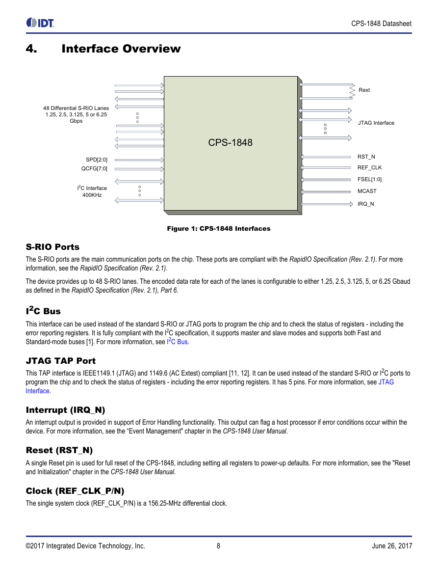
48 Differential S-RIO Lanes
1.25, 2.5, 3.125, 5 or 6.25
Gbps
SPD[2:0]
QCFG[7:0]
I2C Interface
400KHz
CPS-1848
CPS-1848 Datasheet
Rext
JTAG Interface
RST_N
REF_CLK
FSEL[1:0]
MCAST
IRQ_N
Figure 1: CPS-1848 Interfaces
S-RIO Ports
The S-RIO ports are the main communication ports on the chip. These ports are compliant with the RapidIO Specification (Rev. 2.1). For more
information, see the RapidIO Specification (Rev. 2.1).
The device provides up to 48 S-RIO lanes. The encoded data rate for each of the lanes is configurable to either 1.25, 2.5, 3.125, 5, or 6.25 Gbaud
as defined in the RapidIO Specification (Rev. 2.1), Part 6.
I2C Bus
This interface can be used instead of the standard S-RIO or JTAG ports to program the chip and to check the status of registers - including the
error reporting registers. It is fully compliant with the I2C specification, it supports master and slave modes and supports both Fast and
Standard-mode buses [1]. For more information, see I2C Bus.
JTAG TAP Port
This TAP interface is IEEE1149.1 (JTAG) and 1149.6 (AC Extest) compliant [11, 12]. It can be used instead of the standard S-RIO or I2C ports to
program the chip and to check the status of registers - including the error reporting registers. It has 5 pins. For more information, see JTAG
Interface.
Interrupt (IRQ_N)
An interrupt output is provided in support of Error Handling functionality. This output can flag a host processor if error conditions occur within the
device. For more information, see the “Event Management" chapter in the CPS-1848 User Manual.
Reset (RST_N)
A single Reset pin is used for full reset of the CPS-1848, including setting all registers to power-up defaults. For more information, see the "Reset
and Initialization" chapter in the CPS-1848 User Manual.
Clock (REF_CLK_P/N)
The single system clock (REF_CLK_P/N) is a 156.25-MHz differential clock.
©2017 Integrated Device Technology, Inc.
8
June 26, 2017
�



 2023年江西萍乡中考道德与法治真题及答案.doc
 2012年重庆南川中考生物真题及答案.doc
 2013年江西师范大学地理学综合及文艺理论基础考研真题.doc
 2020年四川甘孜小升初语文真题及答案I卷.doc
 2020年注册岩土工程师专业基础考试真题及答案.doc
 2023-2024学年福建省厦门市九年级上学期数学月考试题及答案.doc
 2021-2022学年辽宁省沈阳市大东区九年级上学期语文期末试题及答案.doc
 2022-2023学年北京东城区初三第一学期物理期末试卷及答案.doc
 2018上半年江西教师资格初中地理学科知识与教学能力真题及答案.doc
 2012年河北国家公务员申论考试真题及答案-省级.doc
 2020-2021学年江苏省扬州市江都区邵樊片九年级上学期数学第一次质量检测试题及答案.doc
 2022下半年黑龙江教师资格证中学综合素质真题及答案.doc