7 Series FPGAs and
Zynq-7000 SoC XADC Dual
12-Bit 1 MSPS
Analog-to-Digital Converter
User Guide
UG480 (v1.10.1) July 23, 2018
�
Notice of Disclaimer
The information disclosed to you hereunder (the “Materials”) is provided solely for the selection and use of Xilinx products. To the maximum
extent permitted by applicable law: (1) Materials are made available “AS IS” and with all faults, Xilinx hereby DISCLAIMS ALL
WARRANTIES AND CONDITIONS, EXPRESS, IMPLIED, OR STATUTORY, INCLUDING BUT NOT LIMITED TO WARRANTIES OF
MERCHANTABILITY, NON-INFRINGEMENT, OR FITNESS FOR ANY PARTICULAR PURPOSE; and (2) Xilinx shall not be liable (whether
in contract or tort, including negligence, or under any other theory of liability) for any loss or damage of any kind or nature related to, arising
under, or in connection with, the Materials (including your use of the Materials), including for any direct, indirect, special, incidental, or
consequential loss or damage (including loss of data, profits, goodwill, or any type of loss or damage suffered as a result of any action
brought by a third party) even if such damage or loss was reasonably foreseeable or Xilinx had been advised of the possibility of the same.
Xilinx assumes no obligation to correct any errors contained in the Materials or to notify you of updates to the Materials or to product
specifications. You may not reproduce, modify, distribute, or publicly display the Materials without prior written consent. Certain products are
subject to the terms and conditions of Xilinx’s limited warranty, please refer to Xilinx’s Terms of Sale which can be viewed at
www.xilinx.com/legal.htm#tos; IP cores may be subject to warranty and support terms contained in a license issued to you by Xilinx. Xilinx
products are not designed or intended to be fail-safe or for use in any application requiring fail-safe performance; you assume sole risk and
liability for use of Xilinx products in such critical applications, please refer to Xilinx’s Terms of Sale which can be viewed at
www.xilinx.com/legal.htm#tos.
AUTOMOTIVE APPLICATIONS DISCLAIMER
AUTOMOTIVE PRODUCTS (IDENTIFIED AS “XA” IN THE PART NUMBER) ARE NOT WARRANTED FOR USE IN THE DEPLOYMENT
OF AIRBAGS OR FOR USE IN APPLICATIONS THAT AFFECT CONTROL OF A VEHICLE (“SAFETY APPLICATION”) UNLESS THERE
IS A SAFETY CONCEPT OR REDUNDANCY FEATURE CONSISTENT WITH THE ISO 26262 AUTOMOTIVE SAFETY STANDARD
(“SAFETY DESIGN”). CUSTOMER SHALL, PRIOR TO USING OR DISTRIBUTING ANY SYSTEMS THAT INCORPORATE PRODUCTS,
THOROUGHLY TEST SUCH SYSTEMS FOR SAFETY PURPOSES. USE OF PRODUCTS IN A SAFETY APPLICATION WITHOUT A
SAFETY DESIGN IS FULLY AT THE RISK OF CUSTOMER, SUBJECT ONLY TO APPLICABLE LAWS AND REGULATIONS GOVERNING
LIMITATIONS ON PRODUCT LIABILITY.
© Copyright 2011–2018 Xilinx, Inc. Xilinx, the Xilinx logo, Artix, ISE, Kintex, Spartan, Virtex, Vivado, Zynq, and other designated brands
included herein are trademarks of Xilinx in the United States and other countries. All other trademarks are the property of their respective
owners.
XADC User Guide
www.xilinx.com
UG480 (v1.10.1) July 23, 2018
�
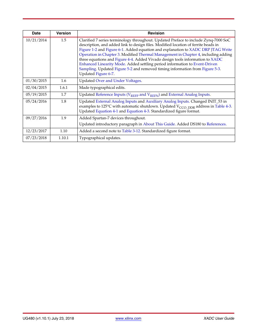
Revision History
The following table shows the revision history for this document.
Date
Version
Revision
03/01/2011
03/28/2011
10/25/2012
1.0
1.1
1.2
Initial Xilinx release.
Added “Dual 12-Bit MSPS Analog-to-Digital Converter” to document title. Modified
first paragraph and added second paragraph in Chapter 1, Introduction and Quick Start.
Added Table 1-1. Removed the Thermal Diode (DXP and DXN) section from Chapter 4.
This version was updated to include information for the Zynq-7000 SoC devices: Added
“Zynq-7000 SoC” to document title.
In Figure 1-1 Zynq-7000 SoC information was added and the control and status registers
changed from 32 x 16 bits to 64 x 16 bits. The System Monitor Support section changed to
Differences between Virtex-5 and Virtex-6 System Monitors. Functionality for the XADC
block in 7 series FPGAs is now defined for previously undefined status registers in
subsequent chapters. Capacitor values in Figure 1-2 changed, and a note was added
about the placement of 100 nF decoupling capacitors. In Table 1-1, for VREFP_0, GND
changed to GNDADC, accurate reference source changed to accurate reference IC, and
VP_0 and VN_0 types were changed to dedicated analog inputs. Footnotes were added to
support 7 series and Zynq device pin packages. A note about application guidelines was
added after Table 1-1. Information about auxiliary analog channels was added to the
External Analog Inputs section. In Table 1-2, ports ALM[0] through [ALM[3] have XADC
removed from the description. Alarms specific to Zynq-7000 SoC devices (ALM[4],
ALM[5], and ALM[6]) were added. The example in Example Instantiation was updated.
In ADC and Sensors, information about an analog input signal of 200 mV was modified,
and Equation 1-1 was added. A new Zynq-7000 SoC subsection was added to the end of
the chapter.
In ADC Transfer Functions MSBs are defined as left-most bits. In Auxiliary Analog
Inputs in the instantiation was changed to on the primitive, and information that
configuration is automatic when analog inputs are connected was added. The Note on
page 29 was expanded to clarify device support of auxiliary analog channels.
Equation 2-2 was added (unipolar mode), Equation 2-1, Equation 2-3, and Equation 2-4
were modified (“10”was changed to “9”), and the paragraph following Equation 2-4 was
added. Information about additional external resistance was added to Unipolar Input
Signals. In Temperature Sensor this sentence was deleted: “The on-chip temperature
sensor has a maximum measurement error of ±4°C over a range of –40°C to +125°C.”
Information was added to the Power Supply Sensor section about which supplies are
monitored and where measurements are stored for Zynq-7000 SoC devices.
UG480 (v1.10.1) July 23, 2018
www.xilinx.com
XADC User Guide
�
Date
10/25/2012
Version
1.2
(Cont’d)
03/10/2014
1.3
04/9/2014
05/31/2014
1.3.1
1.4
Revision
Min/max register lists were updated for Zynq-7000 SoC devices in Figure 3-1. In
Table 3-1 the VREFN description was updated, new Zynq-7000 device channels VCCPINT,
VCCPAUX, and VCCO_DDR were added. Zynq-7000 SoC status registers were added to
Figure 3-1. Flag registers for DI5 through DI8 in Figure 3-2 changed and DIS was
removed from Table 3-2. XADC Calibration Coefficients were added. Configuration
registers ALM[4], ALM[5], and ALM[6] were added to Figure 3-4. In Table 3-3, a new
row was added for bits DI19 to DI11. In Table 3-7, rows for ADC channels 13, 14, and 15
were added. Zynq-7000 SoC alarm threshold register information was added to Alarm
Registers (50h to 5Fh). A note in the section DRP JTAG Interface mentions conditions in
which the external JTAG access is disabled for Zynq devices. Section Zynq-7000 SoC
Processing System (PS) to XADC Dedicated Interface was added to the end of the
chapter.
In XADC Operating Modes, operate both ADCs in parallel in the first paragraph changed
to operate both ADCs in lock step. In Single Channel Mode, the first sentence was deleted
(“Single channel mode is the most basic way users can modify the operation of the
XADC.”) Sequence numbers and descriptions in Table 4-1 and Table 4-2 changed and
were added for Zynq-7000 SoC devices. In Sequencer Modes, default mode sequences
were changed in Table 4-3 and added for Zynq-7000 SoC devices. The sentence before
Table 4-4 was deleted. The footnote in Table 4-4 and Table 4-6 was enhanced to mention
auxiliary analog channel support. Table 4-7 was updated to include Zynq-7000 SoC
channels. Alarm threshold registers for the Zynq-7000 SoC were added to Table 4-8. A
new section XADC Enhanced Linearity Mode and Figure 4-5 were added to the end of
the chapter.
The Dynamic Reconfiguration Port (DRP) Timing section was added. Removed
Table 5-1: XADC Timing Information.
In Reference Inputs (VREFP and VREFN), added “Noise on the reference voltage also adds
noise to the ADC conversion and results in more code transition noise or poorer than
expected SNR” to the end of the first paragraph. Capacitor values were changed, a new
10 µF capacitor was added, and notes were added to Figure 6-1. Notes were added to
Figure 6-5. XADC Software Support was completely replaced. In that section, the Verilog
instantiation was replaced. Figure 6-6: Analog Stimulus File and Figure 6-7: XADC
Simulation Output were deleted. In the new section, Figure 6-5 through Figure 6-8 were
added.
Updated the disclaimer and copyright. Changes to Figure 1-2 in XADC Pinout
Requirements. In External Analog Inputs, clarified how auxiliary analog inputs are
handled in Vivado tools. Improved description of RESET signal in Table 1-2. In
Adjusting the Acquisition Settling Time, added to description of ACQ bit. In Analog
Input Description, added note to Equation 2-1. Added Table 3-3, Calibration Coefficients
in Status Register. Added to description of DI4 and DI5 in Table 3-5. Added to important
note in DRP JTAG Interface. Added clarification to Table 4-1 and Table 4-2 in ADC
Channel Selection Registers (48h and 49h) section. Modified Figure 4-3. Added note to
Table 4-8, Alarm Threshold Registers. Changes to description of Thermal Management.
Modified Figure 5-1. Updated Conversion Phase and Event-Driven Sampling. Added to
description of Acquisition Phase. Updated External Analog Inputs. Modified Figure 6-3.
Modified Example Design Instantiation and Example Design Test Bench. Updated Using
XADC Instantiation Wizard. Updated Figure 6-7.
Updated link to UG585 in References.
Updated Figure 1-2, Figure 2-10, and Figure 3-3. Updated VREFP_0 package pin
description in Table 1-1. Updated Gain Coefficients and Single Pass Mode. Added
second paragraph to Chapter 4, XADC Operating Modes introduction.
XADC User Guide
www.xilinx.com
UG480 (v1.10.1) July 23, 2018
�
Date
Version
10/21/2014
1.5
01/30/2015
02/04/2015
05/19/2015
05/24/2016
1.6
1.6.1
1.7
1.8
09/27/2016
1.9
12/23/2017
07/23/2018
1.10
1.10.1
Revision
Clarified 7 series terminology throughout. Updated Preface to include Zynq-7000 SoC
description, and added link to design files. Modified location of ferrite beads in
Figure 1-2 and Figure 6-1. Added equation and explanation to XADC DRP JTAG Write
Operation in Chapter 3. Modified Thermal Management in Chapter 4, including adding
three equations and Figure 4-4. Added Vivado design tools information to XADC
Enhanced Linearity Mode. Added settling period information to Event-Driven
Sampling. Updated Figure 5-2 and removed timing information from Figure 5-3.
Updated Figure 6-7.
Updated Over and Under Voltages.
Made typographical edits.
Updated Reference Inputs (VREFP and VREFN) and External Analog Inputs.
Updated External Analog Inputs and Auxiliary Analog Inputs. Changed INIT_53 in
examples to 125°C with automatic shutdown. Updated VCCO_DDR address in Table 4-3.
Updated Equation 4-1 and Equation 4-3. Standardized figure format.
Added Spartan-7 devices throughout.
Updated introductory paragraph in About This Guide. Added DS180 to References.
Added a second note to Table 3-12. Standardized figure format.
Typographical updates.
UG480 (v1.10.1) July 23, 2018
www.xilinx.com
XADC User Guide
�
XADC User Guide
www.xilinx.com
UG480 (v1.10.1) July 23, 2018
�
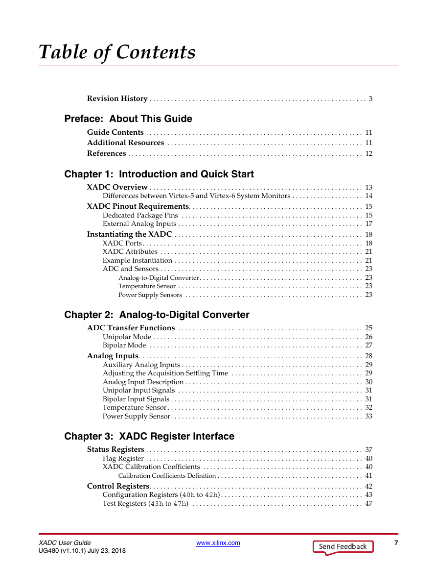
Table of Contents
Revision History . . . . . . . . . . . . . . . . . . . . . . . . . . . . . . . . . . . . . . . . . . . . . . . . . . . . . . . . . . . . . 3
Preface: About This Guide
Guide Contents . . . . . . . . . . . . . . . . . . . . . . . . . . . . . . . . . . . . . . . . . . . . . . . . . . . . . . . . . . . . . 11
Additional Resources . . . . . . . . . . . . . . . . . . . . . . . . . . . . . . . . . . . . . . . . . . . . . . . . . . . . . . . 11
References . . . . . . . . . . . . . . . . . . . . . . . . . . . . . . . . . . . . . . . . . . . . . . . . . . . . . . . . . . . . . . . . . . 12
Chapter 1: Introduction and Quick Start
XADC Overview . . . . . . . . . . . . . . . . . . . . . . . . . . . . . . . . . . . . . . . . . . . . . . . . . . . . . . . . . . . . 13
Differences between Virtex-5 and Virtex-6 System Monitors . . . . . . . . . . . . . . . . . . . . 14
XADC Pinout Requirements. . . . . . . . . . . . . . . . . . . . . . . . . . . . . . . . . . . . . . . . . . . . . . . . . 15
Dedicated Package Pins . . . . . . . . . . . . . . . . . . . . . . . . . . . . . . . . . . . . . . . . . . . . . . . . . . . 15
External Analog Inputs . . . . . . . . . . . . . . . . . . . . . . . . . . . . . . . . . . . . . . . . . . . . . . . . . . . . 17
Instantiating the XADC . . . . . . . . . . . . . . . . . . . . . . . . . . . . . . . . . . . . . . . . . . . . . . . . . . . . . 18
XADC Ports. . . . . . . . . . . . . . . . . . . . . . . . . . . . . . . . . . . . . . . . . . . . . . . . . . . . . . . . . . . . . . 18
XADC Attributes . . . . . . . . . . . . . . . . . . . . . . . . . . . . . . . . . . . . . . . . . . . . . . . . . . . . . . . . . 21
Example Instantiation . . . . . . . . . . . . . . . . . . . . . . . . . . . . . . . . . . . . . . . . . . . . . . . . . . . . . 21
ADC and Sensors . . . . . . . . . . . . . . . . . . . . . . . . . . . . . . . . . . . . . . . . . . . . . . . . . . . . . . . . . 23
Analog-to-Digital Converter. . . . . . . . . . . . . . . . . . . . . . . . . . . . . . . . . . . . . . . . . . . . . . 23
Temperature Sensor . . . . . . . . . . . . . . . . . . . . . . . . . . . . . . . . . . . . . . . . . . . . . . . . . . . . 23
Power Supply Sensors . . . . . . . . . . . . . . . . . . . . . . . . . . . . . . . . . . . . . . . . . . . . . . . . . . 23
Chapter 2: Analog-to-Digital Converter
ADC Transfer Functions . . . . . . . . . . . . . . . . . . . . . . . . . . . . . . . . . . . . . . . . . . . . . . . . . . . . 25
Unipolar Mode . . . . . . . . . . . . . . . . . . . . . . . . . . . . . . . . . . . . . . . . . . . . . . . . . . . . . . . . . . . 26
Bipolar Mode . . . . . . . . . . . . . . . . . . . . . . . . . . . . . . . . . . . . . . . . . . . . . . . . . . . . . . . . . . . . 27
Analog Inputs. . . . . . . . . . . . . . . . . . . . . . . . . . . . . . . . . . . . . . . . . . . . . . . . . . . . . . . . . . . . . . . 28
Auxiliary Analog Inputs . . . . . . . . . . . . . . . . . . . . . . . . . . . . . . . . . . . . . . . . . . . . . . . . . . . 29
Adjusting the Acquisition Settling Time . . . . . . . . . . . . . . . . . . . . . . . . . . . . . . . . . . . . . 29
Analog Input Description . . . . . . . . . . . . . . . . . . . . . . . . . . . . . . . . . . . . . . . . . . . . . . . . . . 30
Unipolar Input Signals . . . . . . . . . . . . . . . . . . . . . . . . . . . . . . . . . . . . . . . . . . . . . . . . . . . . 31
Bipolar Input Signals . . . . . . . . . . . . . . . . . . . . . . . . . . . . . . . . . . . . . . . . . . . . . . . . . . . . . . 31
Temperature Sensor . . . . . . . . . . . . . . . . . . . . . . . . . . . . . . . . . . . . . . . . . . . . . . . . . . . . . . . 32
Power Supply Sensor. . . . . . . . . . . . . . . . . . . . . . . . . . . . . . . . . . . . . . . . . . . . . . . . . . . . . . 33
Chapter 3: XADC Register Interface
Status Registers . . . . . . . . . . . . . . . . . . . . . . . . . . . . . . . . . . . . . . . . . . . . . . . . . . . . . . . . . . . . . 37
Flag Register . . . . . . . . . . . . . . . . . . . . . . . . . . . . . . . . . . . . . . . . . . . . . . . . . . . . . . . . . . . . . 40
XADC Calibration Coefficients . . . . . . . . . . . . . . . . . . . . . . . . . . . . . . . . . . . . . . . . . . . . . 40
Calibration Coefficients Definition . . . . . . . . . . . . . . . . . . . . . . . . . . . . . . . . . . . . . . . . . 41
Control Registers. . . . . . . . . . . . . . . . . . . . . . . . . . . . . . . . . . . . . . . . . . . . . . . . . . . . . . . . . . . . 42
Configuration Registers (40h to 42h) . . . . . . . . . . . . . . . . . . . . . . . . . . . . . . . . . . . . . . . . 43
Test Registers (43h to 47h) . . . . . . . . . . . . . . . . . . . . . . . . . . . . . . . . . . . . . . . . . . . . . . . . 47
XADC User Guide
UG480 (v1.10.1) July 23, 2018
www.xilinx.com
7
Send Feedback�
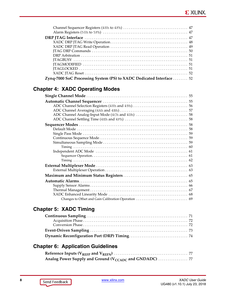
Channel Sequencer Registers (48h to 4Fh) . . . . . . . . . . . . . . . . . . . . . . . . . . . . . . . . . . . 47
Alarm Registers (50h to 5Fh) . . . . . . . . . . . . . . . . . . . . . . . . . . . . . . . . . . . . . . . . . . . . . . 47
DRP JTAG Interface . . . . . . . . . . . . . . . . . . . . . . . . . . . . . . . . . . . . . . . . . . . . . . . . . . . . . . . . 47
XADC DRP JTAG Write Operation . . . . . . . . . . . . . . . . . . . . . . . . . . . . . . . . . . . . . . . . . . 48
XADC DRP JTAG Read Operation . . . . . . . . . . . . . . . . . . . . . . . . . . . . . . . . . . . . . . . . . . 49
JTAG DRP Commands . . . . . . . . . . . . . . . . . . . . . . . . . . . . . . . . . . . . . . . . . . . . . . . . . . . . 50
DRP Arbitration . . . . . . . . . . . . . . . . . . . . . . . . . . . . . . . . . . . . . . . . . . . . . . . . . . . . . . . . . . 51
JTAGBUSY . . . . . . . . . . . . . . . . . . . . . . . . . . . . . . . . . . . . . . . . . . . . . . . . . . . . . . . . . . . . . . 51
JTAGMODIFIED . . . . . . . . . . . . . . . . . . . . . . . . . . . . . . . . . . . . . . . . . . . . . . . . . . . . . . . . . 51
JTAGLOCKED . . . . . . . . . . . . . . . . . . . . . . . . . . . . . . . . . . . . . . . . . . . . . . . . . . . . . . . . . . . 51
XADC JTAG Reset . . . . . . . . . . . . . . . . . . . . . . . . . . . . . . . . . . . . . . . . . . . . . . . . . . . . . . . . 52
Zynq-7000 SoC Processing System (PS) to XADC Dedicated Interface . . . . . . . . 52
Chapter 4: XADC Operating Modes
Single Channel Mode . . . . . . . . . . . . . . . . . . . . . . . . . . . . . . . . . . . . . . . . . . . . . . . . . . . . . . . 55
Automatic Channel Sequencer . . . . . . . . . . . . . . . . . . . . . . . . . . . . . . . . . . . . . . . . . . . . . . 55
ADC Channel Selection Registers (48h and 49h) . . . . . . . . . . . . . . . . . . . . . . . . . . . . . . 56
ADC Channel Averaging (4Ah and 4Bh) . . . . . . . . . . . . . . . . . . . . . . . . . . . . . . . . . . . . . 57
ADC Channel Analog-Input Mode (4Ch and 4Dh) . . . . . . . . . . . . . . . . . . . . . . . . . . . . 58
ADC Channel Settling Time (4Eh and 4Fh) . . . . . . . . . . . . . . . . . . . . . . . . . . . . . . . . . . 58
Sequencer Modes . . . . . . . . . . . . . . . . . . . . . . . . . . . . . . . . . . . . . . . . . . . . . . . . . . . . . . . . . . . 58
Default Mode . . . . . . . . . . . . . . . . . . . . . . . . . . . . . . . . . . . . . . . . . . . . . . . . . . . . . . . . . . . . 58
Single Pass Mode . . . . . . . . . . . . . . . . . . . . . . . . . . . . . . . . . . . . . . . . . . . . . . . . . . . . . . . . . 59
Continuous Sequence Mode . . . . . . . . . . . . . . . . . . . . . . . . . . . . . . . . . . . . . . . . . . . . . . . . 59
Simultaneous Sampling Mode . . . . . . . . . . . . . . . . . . . . . . . . . . . . . . . . . . . . . . . . . . . . . . 59
Timing . . . . . . . . . . . . . . . . . . . . . . . . . . . . . . . . . . . . . . . . . . . . . . . . . . . . . . . . . . . . . . 60
Independent ADC Mode . . . . . . . . . . . . . . . . . . . . . . . . . . . . . . . . . . . . . . . . . . . . . . . . . . 61
Sequencer Operation. . . . . . . . . . . . . . . . . . . . . . . . . . . . . . . . . . . . . . . . . . . . . . . . . . . . 61
Timing . . . . . . . . . . . . . . . . . . . . . . . . . . . . . . . . . . . . . . . . . . . . . . . . . . . . . . . . . . . . . . 62
External Multiplexer Mode . . . . . . . . . . . . . . . . . . . . . . . . . . . . . . . . . . . . . . . . . . . . . . . . . . 63
External Multiplexer Operation . . . . . . . . . . . . . . . . . . . . . . . . . . . . . . . . . . . . . . . . . . . . . 63
Maximum and Minimum Status Registers . . . . . . . . . . . . . . . . . . . . . . . . . . . . . . . . . . . 65
Automatic Alarms. . . . . . . . . . . . . . . . . . . . . . . . . . . . . . . . . . . . . . . . . . . . . . . . . . . . . . . . . . . 65
Supply Sensor Alarms . . . . . . . . . . . . . . . . . . . . . . . . . . . . . . . . . . . . . . . . . . . . . . . . . . . . . 66
Thermal Management . . . . . . . . . . . . . . . . . . . . . . . . . . . . . . . . . . . . . . . . . . . . . . . . . . . . . 67
XADC Enhanced Linearity Mode . . . . . . . . . . . . . . . . . . . . . . . . . . . . . . . . . . . . . . . . . . . 68
Changes to Offset and Gain Calibration Operation . . . . . . . . . . . . . . . . . . . . . . . . . . . . 69
Chapter 5: XADC Timing
Continuous Sampling . . . . . . . . . . . . . . . . . . . . . . . . . . . . . . . . . . . . . . . . . . . . . . . . . . . . . . . 71
Acquisition Phase. . . . . . . . . . . . . . . . . . . . . . . . . . . . . . . . . . . . . . . . . . . . . . . . . . . . . . . . . 72
Conversion Phase . . . . . . . . . . . . . . . . . . . . . . . . . . . . . . . . . . . . . . . . . . . . . . . . . . . . . . . . . 72
Event-Driven Sampling . . . . . . . . . . . . . . . . . . . . . . . . . . . . . . . . . . . . . . . . . . . . . . . . . . . . . 73
Dynamic Reconfiguration Port (DRP) Timing. . . . . . . . . . . . . . . . . . . . . . . . . . . . . . . . 74
Chapter 6: Application Guidelines
Reference Inputs (VREFP and VREFN) . . . . . . . . . . . . . . . . . . . . . . . . . . . . . . . . . . . . . . . . 77
Analog Power Supply and Ground (VCCADC and GNDADC) . . . . . . . . . . . . . . . . 77
8
www.xilinx.com
XADC User Guide
UG480 (v1.10.1) July 23, 2018
Send Feedback�



 2023年江西萍乡中考道德与法治真题及答案.doc
 2012年重庆南川中考生物真题及答案.doc
 2013年江西师范大学地理学综合及文艺理论基础考研真题.doc
 2020年四川甘孜小升初语文真题及答案I卷.doc
 2020年注册岩土工程师专业基础考试真题及答案.doc
 2023-2024学年福建省厦门市九年级上学期数学月考试题及答案.doc
 2021-2022学年辽宁省沈阳市大东区九年级上学期语文期末试题及答案.doc
 2022-2023学年北京东城区初三第一学期物理期末试卷及答案.doc
 2018上半年江西教师资格初中地理学科知识与教学能力真题及答案.doc
 2012年河北国家公务员申论考试真题及答案-省级.doc
 2020-2021学年江苏省扬州市江都区邵樊片九年级上学期数学第一次质量检测试题及答案.doc
 2022下半年黑龙江教师资格证中学综合素质真题及答案.doc