logo资料库

Intel CPU设计指导书.pdf

第1页 / 共593页
第2页 / 共593页
第3页 / 共593页
第4页 / 共593页
第5页 / 共593页
第6页 / 共593页
第7页 / 共593页
第8页 / 共593页
资料共593页,剩余部分请下载后查看
Kaby Lake H Platform
Contents
Figures
Tables
Revision History
1 Introduction
1.1 Terminology
1.2 Reference Documents
2 Stack-Up and PCB Considerations
2.1 Printed Circuit Board Considerations
2.2 Generalized 8-Layer Motherboard Example
2.3 Generalized 10-Layer Motherboard Example
2.4 Single-Ended and Differential-Impedance Transmission Line Specifications
2.4.1 Breakout Geometries
2.4.2 Routing Geometries
2.5 Low Halogen Flame Retardant Stack-Up Considerations
2.5.1 Choosing a Low Halogen Material
2.5.2 Electrical Limits of Low Halogen Material Properties
2.6 Reference Planes
2.7 Type 4 PCB Vias
2.7.1 Plated Through Hole, Buried Via, and Microvia Dimensions
2.7.2 Staggered versus Stacked Microvias
2.7.3 Buried Via to Microvia Keep-Out
2.8 Backward and Forward Coupling Coefficient Calculation
2.9 Minimizing the Effect of Fiber Weave
2.9.1 Overview of Fiber Weave
2.9.2 Fiber Weave Effect versus Transfer Rate and Trace Length
2.9.3 Specific Routing Configurations
2.9.4 Offset Routing
2.9.5 Zig-Zag or Slanted Routing
2.9.6 Image Rotation
2.9.7 Using Alternate PCB Materials
2.10 Flexible Printed Circuit Consideration
2.11 Kaby Lake Client Signal Integrity Tool Suite
3 General Differential Design Guidelines
3.1 General Differential Stackup Guidelines
3.1.1 Stackup and Layer Utilization Guidelines
3.2 General Differential Routing Guidelines
3.2.1 Breakout Example and Guidelines
3.2.2 Differential I/O Routing Scheme Guidelines
3.3 General Differential Optimization Guidelines
3.3.1 Via Placement and Via Usage Optimization
3.3.2 Bend Optimization Guidelines
3.3.3 Component Footprint Optimization Guidelines
3.3.4 General Routing Guidelines
3.4 General Differential Length Matching Guidelines
3.4.1 Length Matching and Length Formulas
3.5 General Differential Compensation and Voltage Reference Guidelines
3.5.1 RCOMP Signal Guidelines
3.5.2 Reference Planes
3.6 General Docking Connector Recommendations for Differential Interfaces
4 System Memory Interface Design Guidelines
4.1 KBL-H DDR4 ECC SO-DIMM 2DPC Guidelines
4.1.1 Stub Reduction and Alternative Pin Map
4.2 KBL-H DDR4 SO-DIMM 2DPC Guidelines
4.3 KBL-H DDR4 SO-DIMM 1DPC Guidelines
4.4 KBL-H DDR4 1R x16 Memory Down Guidelines
4.5 KBL-H DDR4 1R x16 Double-T Topology Memory Down Guidelines
4.6 KBL-H DDR4 2R x8 Memory Down Guidelines
4.7 KBL-H LPDDR3 x32 Memory Down
4.8 KBL-H DDR4 ECC SO-DIMM 1DPC Guidelines
4.9 KBL-H System Memory ODT Signal Connectivity Details
4.10 Memory Data Mask (DM) Signals Connectivity Details
4.11 .KBL H System Memory Via Placement and Pad Optimization Guidelines
4.11.1 Via Placement at CPU Side
4.11.2 Via Placement at SO-DIMM and DRAM Device Side
4.12 KBL H System Memory Reference Voltage (VREF) Guidelines
4.13 KBL-H DDR Power Delivery - Memory side
4.13.1 KBL-H DDR4 SODIMM Decoupling
4.13.2 KBL-H DDR4 Memory Down Decoupling
4.13.3 KBL-H LPDDR3 x32 Memory Down Decoupling
5 DisplayPort* Design Guidelines
5.1 Introduction
5.1.1 DisplayPort* Link Bit Rates
5.1.2 DisplayPort* Main Link Buffer Type
5.1.3 Reference Documents
5.2 DisplayPort* Signal Descriptions
5.2.1 Signal Groups
5.3 DisplayPort* Topology Guidelines
5.3.1 Optimizations
5.3.2 DisplayPort* Main Link Motherboard and Main Link
5.3.3 Display Port* Main Link on Dock Topology with Redriver
5.3.4 DisplayPort* Internal Cabled Solution
5.3.5 DisplayPort* Auxiliary Channel Topologies
5.4 DisplayPort* General Considerations and Optimization
5.4.1 AUX-CH Stack-up Guidelines
5.4.2 DisplayPort* HPD General Considerations and Optimization
5.4.3 DisplayPort* Main Link Differential-Pair Width and Spacing
5.4.4 DisplayPort* Auxiliary Channel (AUX CH) General Design Considerations and Optimization
5.5 DisplayPort* Length Matching Guidelines
5.6 Digital Display Interface Disabling and Termination Guidelines
5.7 Display Compensation Guidelines
6 Embedded DisplayPort* (eDP*) Design Guidelines
6.1 Signal Descriptions
6.2 Topology Guidelines
6.3 Optimizations
6.3.1 Kaby Lake Processor Graphics Embedded DisplayPort* Main Link Topology for HBR and HBR2
6.3.2 Embedded DisplayPort* to VGA Main Link Topology
6.3.3 Kaby Lake Processor Graphics eDP* Auxiliary Channel Topology
6.3.4 KBL Embedded Display Port Aux Channel DP to VGA Converter Topology A
6.3.5 Embedded DisplayPort* Hot-Plug Detect Implementation
6.4 Length Matching Guidelines
6.5 Digital Display Interface Compensation Guidelines
6.5.1 Compensation Signal Routing Guidelines
6.5.2 Disabling and Termination Guidelines
7 High-Definition Multimedia Interface* (HDMI*) Design Guidelines
7.1 Overview
7.2 Signal Description
7.3 HDMI 1.4* Topology Guidelines
7.3.1 Differential-Pair Width and Spacing
7.3.2 Optimizations
7.3.3 HDMI 1.4* Main Link Cost-reduced Level Shifter and Active Level Shifter Topologies
7.3.4 HDMI 1.4* (DDC) Signals Design Guidelines
7.3.5 HDMI 1.4* DDC Signals on Motherboard Topologies with Cost-reduced Level Shifter, Active Level Shifter and Docking Active Level Shifter
7.3.6 HDMI 1.4* HPD Implementation
7.4 HDMI* 2.0 Topology Guidelines
7.4.1 HDMI 2.0* HPD Implementation
7.5 Digital Display Interface Disabling and Termination Guidelines
7.6 Display Compensation Guidelines
8 Processor - PCI Express* Design Guidelines
8.1 Introduction
8.1.1 Compliance Documents
8.2 Signal Description
8.3 Topologies Guidelines
8.4 General Routing Guidelines
8.4.1 Reference Planes
8.4.2 Lane to Controller Allocation
8.5 Slot Reset Implementation
8.6 Debug Guidelines
8.6.1 Probe Points for Testing Soldered Down PCI Express* Devices
8.6.2 Passive Components
8.7 Compensation Guidelines
9 Direct Media Interface Design Guidelines
9.1 Introduction
9.1.1 Compliance Specification
9.2 Signal Descriptions
9.3 Topology Guidelines
9.3.1 Differential-Pair Width and Spacing
9.3.2 DMI 2-Via Topology
9.4 Configuration
9.4.1 Lane Reversal and Polarity Inversion Support
9.5 Compensation Guidelines
10 Switchable Graphics Design Guidelines
10.1 Introduction
10.2 Additional Guidelines
10.2.1 GPIO Selection Criteria
10.2.2 Enabling Switchable Graphics on Reference Validation Platform (RVP)
11 Thunderbolt™ Design Guidelines
11.1 Supported Thunderbolt™ Configuration Options
11.2 Port Power Requirements
11.2.1 Host Source Requirements
11.3 Power Delivery
11.3.1 Power Provider VBUS Electrical Requirements
11.3.2 VCONN Source Electrical Requirements
11.3.3 BIOS
11.3.4 Reference Documents
11.3.5 Compliance Specification
11.3.6 Signal Descriptions
11.4 Topology Guidelines
11.4.1 Motherboard Down Topology
11.4.2 DisplayPort* to Thunderbolt™ Topology
11.4.3 Add-In Card Topology
11.4.4 Connector Guideline
11.5 Length Matching Guidelines
11.6 Stack-up Guidelines
11.6.1 Stack-up and Layer Utilization Guidelines
11.6.2 Thunderbolt™ Insertion Loss Spec
11.7 Optimization Guidelines
11.7.1 TBT Lane Routing and Component Placement
11.7.2 Via Placement and Via Pad Optimization
11.8 Debug Guidelines
11.8.1 PCIe* and DisplayPort* Configuration
11.8.2 NVM Configuration
11.9 Additional Guidelines
11.9.1 Crystal Design Requirement
11.9.2 NVM
12 Asynchronous and Sideband Signals Design Guidelines
12.1 Signal Descriptions
12.1.1 Signal Groups
12.2 Topology Guidelines
12.2.1 PROCHOT# Topology
12.2.2 CATERR# Topology
12.2.3 PROCPWRGD Topology
12.2.4 VCCST_PWRGOOD Topology
12.2.5 THERMTRIP# Topology
12.2.6 RESET# (PLTRST#) Topology
12.2.7 Platform Environmental Control Interface (PECI) Topology
12.2.8 BPM#[3:0] Topology
12.2.9 PM_SYNC Topology
12.2.10 PM_DOWN Topology
12.2.11 PROC_TRIGIN Topology (PCH to Processor_TRIGIN)
12.2.12 PROC_TRIGOUT Topology (Processor to PCH_TRIGIN)
12.2.13 SVID Topology
12.2.14 COMP Signals
12.3 ESD Protection for Asynchronous Signals
13 Flexible I/O
13.1 Introduction
13.2 Flexible I/O Implementation
13.2.1 U Kaby Lake PCH-H
13.3 HSIO Lane Selection
13.3.1 PCIe*/SATA Lane Selection
13.4 HSIO Board Routing
14 PCI Express* Interface Design Guidelines
14.1 Introduction
14.1.1 Intel® Rapid Storage Technology (Intel® RST) for PCIe* Storage
14.2 PCI Express* Guideline Terminology and Descriptions
14.2.1 PCI Express* Signal Descriptions
14.3 PCI Express* Routing Guidelines
14.3.1 PCI Express* Device Down Guidelines
14.3.2 PCI Express* Connector (ExpressCard* / PCI Express* Mini-Card) Guidelines
14.3.3 PCI Express* with Internal Cable Guidelines
14.3.4 PCI Express* M.2 Socket Module Guidelines
14.3.5 PCI Express* Impedance Compensation Guidelines
14.3.6 PCI Express* Lane Polarity Inversion
14.3.7 PCI Express* Controller Lane Reversal
15 Serial ATA (SATA), mSATA, eSATA and SATA Express Design Guidelines
15.1 Signal Description
15.1.1 SATA Signal Groups
15.1.2 SATA General Purpose (SATAGP[5:0]) Signals
15.1.3 DEVSLP[5:0] Implementation
15.1.4 SATALED# Implementation
15.2 General Guidelines
15.2.1 General SATA Routing Guidelines
15.2.2 SATA Trace Separation
15.2.3 SATA Configuration, Connectivity, Block Diagram
15.2.4 Optimization Guidelines
15.2.5 SATA Differential Length Matching Guidelines
15.2.6 SATA Decoupling Guidelines
15.2.7 SATA Debug Guidelines
15.2.8 SATA Additional Guidelines
15.2.9 SATA Disabling and Termination Guidelines
15.3 Topologies and Guidelines
15.3.1 mSATA and Direct Connect Topology
15.3.2 eSATA Topology
15.3.3 Internal SATA Topology (Cable Connect)
15.3.4 SATA Express Topology
16 Universal Serial Bus 3.0 Design Guidelines
16.1 Signal Descriptions
16.1.1 Signal Groups
16.1.2 Overcurrent Protection
16.2 Topology Guidelines
16.2.1 Back Panel USB 3.0 Back Panel Topology
16.2.2 USB 3.0 Front Panel Topology
16.2.3 Traditional Docking Topology
16.2.4 USB 3.0 ExpressCard* Topology
16.3 Stackup Guidelines
16.3.1 Stackup and Layer Utilization Guidelines
16.3.2 Stub Guidelines
16.3.3 USB 3.0* Non-interleaved Breakout Guidelines
16.3.4 Length Matching and Length Formulas
16.4 Optimization Guidelines
16.4.1 USB Connector/Receptacle Recommendations
16.4.2 Internal USB Cables
16.4.3 Internal Cable Daughter Card
16.4.4 Design Risk Minimization Approaches
16.5 EMC Component Selection Guidelines
16.6 USB Port Extension
16.7 Disabling and Termination Guidelines
17 Universal Serial Bus 2.0 Design Guidelines
17.1 Signal Descriptions
17.1.1 USB 2.0 Signal Groups
17.1.2 USBCOMP Connection Guidelines
17.1.3 USBCOMP Routing Guidelines
17.1.4 USBCOMP to Other Interfaces
17.1.5 Overcurrent Protection
17.2 USB 2.0 Topology Guidelines
17.2.1 Back Panel/External Topology
17.2.2 USB 2.0 Internal Cable Topology/Front Panel Topology
17.2.3 USB 2.0 Device Down Topology
17.2.4 USB 2.0 External / Back Panel with Power Switch / BC1.2 Charger Module / MUX Topology
17.2.5 USB 2.0 Docking Topology
17.2.6 USB Connector Recommendations
17.2.7 Daughter Card
17.3 Stack-up Guidelines
17.3.1 Stack-up and Layer Utilization Guidelines
17.4 Configuration, Connectivity, Block Diagram
17.4.1 USB 3.0/2.0 Port Pairing
17.4.2 Port Power Delivery
17.5 Length Matching Guidelines
17.5.1 Length Matching and Length Formulas
17.6 Additional Guidelines
17.6.1 EMI and ESD Protection
17.7 Disabling and Termination Guidelines
18 USB Type-C Design Guidelines
18.1 Introduction
18.2 Supported Configuration
18.2.1 USB Only Configuration
18.3 Single Dual-role (Device Mode) Port Capable USB Type-C over Front Panel
18.4 Alternate Modes Configuration
18.4.1 USB with DP* as Alternate Mode
18.5 Debug
18.6 Power Delivery
18.6.1 USB Type-C VBUS and VCONN Control
18.6.2 USB Type-C VBUS Options
18.7 EMI and ESD Considerations
18.7.1 Common Mode Chokes
18.7.2 USB Type-C Receptacle Selection Recommendations for EMI, RFI Mitigation
18.7.3 ESD Protection
18.8 Overcurrent Protection
18.9 Layout Optimization
18.9.1 CC Pins Layout
18.9.2 Type-C Connector Footprint Voiding Guideline
19 I2C* Interface Design Guidelines
19.1 Signal Descriptions
19.1.1 Signal Groups
19.2 Topology Guidelines
19.2.1 General Design Considerations
19.2.2 I2C* Voltage Signaling Support
19.2.3 Detailed Routing Requirements
19.2.4 Length Matching Requirement
19.3 Additional Guidelines
19.4 Terminating Unused I2C Signals
20 Secure Digital Card with Extended Capacity (SDXC) Interface Design Guidelines
20.1 SDXC Signal Groups
20.2 SDXC Topology Guidelines
20.3 Terminating Unused SDXC Signals
20.4 EMI and ESD Guidance
21 Universal Asynchronous Receiver Transmitter (UART) Interface Design Guidelines
21.1 Signal Descriptions
21.1.1 Signal Groups
21.2 Topology Guidelines
21.3 Terminating Unused UART Signals
22 Generic Serial Peripheral Interface (GSPI)
22.1 Introduction
22.2 Signal Descriptions
22.2.1 Signal Groups
22.3 Topology Guidelines
22.3.1 Length Matching Requirements
22.4 Terminating Unused GSPI Signals
23 Enhanced Serial Peripheral Interface (eSPI)
23.1 Introduction
23.2 Topology and Guidelines
23.2.1 Topology
23.2.2 Routing Guidelines
24 SMBus 2.0/SMLink Interface Design Guidelines
24.1 SMBus 2.0 Introduction
24.2 SMLink Introduction
24.3 Signal Descriptions
24.3.1 Signal Groups
24.4 Topology Guidelines
24.4.1 General Design Considerations
24.4.2 Detailed Routing Requirements
24.4.3 Length Matching Requirements
24.5 Connectivity Recommendation
24.5.1 High Power/Low Power Mixed Architecture
24.6 Additional Guidelines
24.6.1 SMBus Design Considerations
24.6.2 Calculating Physical Segment Pull-Up Resistor
24.6.3 Intel® Trace Hub Backup: SMBus Test Points
25 Low Pin Count (LPC) Interface Design Guidelines
25.1 Overview
25.2 Signal Description
25.3 LPC Topology Guidelines
25.3.1 LPC DATA 3 Load Daisy Chain Topology Guidelines
25.3.2 LPC CLK single load Topology
25.3.3 Disable Guidelines
25.3.4 General Guidelines for Length Matching Requirements
25.3.5 General Guidelines
26 Serial Peripheral Interface (SPI) Flash Design Guidelines
26.1 Introduction
26.2 Topology Guidelines
26.2.1 SPI Single Flash Device Topology Guidelines
26.2.2 Dual SPI Devices + TPM Topology Guidelines
26.2.3 Terminating Unused SPI Signals
26.2.4 SPI Dual Footprint—SO8 and SO16 Packages
26.3 FWH Interface
26.3.1 Decoupling
26.3.2 FWH VPP Design Guidelines
26.4 TPM on SPI
27 Platform Clock Design Guidelines
27.1 Platform Clock Guidelines
27.1.1 Debug Differential Clock Routing Guidelines
27.1.2 Processor Differential Clock Routing Guidelines
27.1.3 SRC Differential Clock Routing Guidelines to Add-in Card
27.1.4 SRC Differential Clock to Down Device Routing Guidelines
27.1.5 Single-Ended Clock Routing Guidelines
27.2 Platform Clock Associated Signal Guidelines
27.2.1 SRC Clock Request Routing Guidelines
27.2.2 24-MHz Crystal and Associated RC Component Routing Guidelines
27.3 XCLK_BIASREF Guidelines
28 Intel® High Definition Audio (Intel® HD Audio) Design Guidelines
28.1 Intel® High Definition Audio (Intel® HD Audio), DMIC, and I2S* Interface Signal Descriptions
28.1.1 Signal Groups
28.2 Intel® High Definition Audio (Intel® HD Audio) and DMIC Topology Guidelines
28.2.1 Intel® HD Audio and DMIC Single Load Audio Device Down Topology
28.2.2 High Definition Audio and DMIC – HDA_SDO/HDA_SYNC/ HDA_BCLK /HDA_RST#/DMIC_CLK/DMIC_DATA Branched Device Topology
28.2.3 Integrated CODEC for Embedded Display (HDMI/DP) Audio
28.2.4 Disabling and Termination Guidelines for High Definition Audio Interface
28.3 Intel® I2S* Topology Guidelines
28.3.1 I2S* Device Connection Topology
29 Intel® Management Engine (Intel® ME) Design Guidelines
29.1 Acronyms and General Terminology
29.2 Reference Documents
29.3 Preface
29.4 Signal Descriptions
29.4.1 Intel® ME to Embedded Controller Interface Signals
29.5 Optimization Guidelines
29.5.1 Intel® ME Guidelines
29.5.2 LAN Considerations with or without Intel® Active Management (Intel® AMT) Support
29.5.3 WLAN Considerations with Intel® Active Management (Intel® AMT) Support
29.5.4 SPI Flash Descriptor Security Override
29.5.5 Intel® Automatic Power Switch (Intel® APS)
29.6 Schematics Design Checklists
29.6.1 Overview
29.6.2 Intel® ME Checklists
30 Real Time Clock (RTC) Design Guidelines
30.1 Real Time Clock Signal Description
30.1.1 Signal Groups
30.1.2 SUSCLK
30.2 Real Time Clock Topology Guidelines
30.2.1 VCCRTC External Circuit
30.2.2 General RTC Layout Considerations
30.2.3 External Capacitors
30.3 RTC External Battery Connection
30.4 RTC External RTCRST# Circuit
30.5 RTC External SRTCRST# Circuit
30.6 RTC-Well Input Strap Requirements
31 Intel® Integrated Sensor Solution
31.1 Introduction
31.2 Detailed Sensors Data
31.3 Design Guidelines and Checklists
32 Discrete Trusted Platform Module (TPM) Design Guidelines
32.1 Signal Description
32.1.1 Signal Groups
33 Platform Reset Considerations
33.1 Signal Description
33.1.1 Signal Groups
33.2 Additional Guidelines
33.2.1 SYS_RESET# Usage Model
33.2.2 SLP_A# Usage Model
33.2.3 SLP_S0# Usage Model
33.2.4 SLP_S3# Usage Model
33.2.5 SLP_S4# Usage Model
33.2.6 SLP_S5# Usage Model
33.2.7 SLP_LAN# Usage Model
33.2.8 SLP_WLAN# Usage Model
33.2.9 SLP_SUS# Usage Model
33.2.10 SUSWARN# / SUSPWRDNACK Usage Model
33.2.11 SUSACK# Usage Model
33.2.12 PWRBTN# Usage Model
33.2.13 PLTRST# Usage Model
33.2.14 SUSCLK Usage Model
33.2.15 RSMRST# Generation
33.2.16 DSW_PWROK Generation
33.2.17 PCH_PWROK Generation
33.2.18 SYS_PWROK Generation
33.2.19 Legacy Requirements
33.2.20 Additional Power Sequencing Considerations
34 Interrupt Interface Design Guidelines
34.1 Signal Description
34.2 Additional Guidelines
34.2.1 PIRQ Routing Example
35 Critical Low Speed Signals Design Guidelines
35.1 Signal Description
35.1.1 Signals Group
35.2 Additional Guidelines
36 M.2 - Next Generation Form Factor (NGFF)
36.1 Introduction
36.1.1 Reference Specifications
36.2 Supported M.2 Features in Kaby Lake
36.2.1 Connector Keys
36.2.2 Module Stand-off
36.2.3 Schematics Connector Symbol - Design Considerations
36.3 Design Guidelines
36.3.1 PCI Express* Interface
36.3.2 SATA and PCI Express* Storage Interface
36.3.3 USB 3.0 Interface
36.3.4 USB 2.0 Interface
36.3.5 SMBus and I2C Topology Guidelines
36.3.6 UART, SDIO and SPI Topology Guidelines
36.3.7 DisplayPort* Topology Guidelines
37 Front Facing HD/FHD Webcam Design Guidelines
37.1 Design Considerations
38 LAN Design Considerations and Guidelines
39 Wireless Modules and Antenna Design Guidelines
39.1 Antenna Integration into Platform
39.1.1 Antenna Placement Options
39.1.2 Antenna Placement for Devices with Multiple Modes of Operation (Convertibles)
39.1.3 Convertible Ultrabooks™—Definition of Lid Modes for the Purpose of Antenna Metric Evaluation
39.2 WLAN RF Integration Recommendations
39.3 WWAN-LTE RF System Integration Recommendations
39.4 Bluetooth* RF System Integration Recommendations
39.5 Wireless Charging Integration Requirements
40 Platform Telecom Design Guidelines
40.1 Safety Rules
40.2 EMC Rules and Regulations
40.3 Telecom Safety Considerations
40.4 Configuration
40.4.1 Isolation
40.4.2 Surge
40.4.3 Example of Wrong Implementation
40.5 Additional Guidelines
41 Platform Power Sequencing Specification
41.1 PCH_PWROK, SYS_PWROK and Other PWRGD Signal Generation
41.2 Sequencing Interface Signals List and Power Rails
41.3 Power States
41.4 Power Sequencing Timing Diagrams—Legacy Signals
41.4.1 Power Sequencing Timing Requirements
41.5 Additional Power Optimizations with Respect to VCCST Rail in S3
41.6 Rail-to-Rail Power Sequencing Requirements
41.6.1 Rail-to-Rail Sequencing For Various Supplies
41.6.2 RSMRST#/DSW_PWROK Special Considerations
41.6.3 Surprise Power Down Sequencing Considerations
41.6.4 eSPI Considerations for Sequencing
42 Platform Debug and Test Hooks
42.1 Platform Debug Port Options
42.1.1 Primary Debug Port Debug Port Routing Guidelines
42.1.2 Secondary Debug Port Routing Guidelines
42.1.3 Intel® DCI Implementation
42.1.4 eXtended Debug Port (XDP) Mechanical Specifications
42.1.5 Chassis Mount Connector (CMC) Mechanical Specifications
42.1.6 Additional Debug Port PCB Layout Guidelines
42.1.7 Additional Routing Guidelines to support Intel® Silicon View Technology (Intel® SVT) based DFM HVM Test Solution
42.1.8 Depopulation Guidelines for Debug Port
43 Design for Testability (DFT)
43.1 Non-Critical to Function Pins (NCTF)
43.2 Manufacturing Test DFT
43.2.1 XDP Connector Pins
43.2.2 Power Up Control Signals
43.2.3 Power Nets
43.2.4 Frequency Pins
43.2.5 Programming Device Pins
43.2.6 Postcode/Error Monitoring
43.2.7 On Board Battery
43.2.8 Miscellaneous
44 Platform Thermal Management Design Guidelines
44.1 Platform Thermal Management Signal Descriptions
44.1.1 Signal Groups
44.2 Platform Thermal Management Configuration, Connectivity, Block Diagram
45 Electromagnetic Compatibility
45.1 General Considerations
45.1.1 Ground Ring/ PTH
45.1.2 Power Plane Decoupling
45.1.3 Connector Decoupling
45.1.4 Crossing Split planes
45.1.5 Reference Discontinuity
45.2 Power Supply
45.2.1 Voltage Regulator
45.2.2 AC Jack
45.3 CPU/ PCH Noise
45.3.1 5760-MHz Noise
45.4 Critical Signals
45.4.1 Audio
45.4.2 LPC
45.4.3 Integrated Touch (SPI)
45.4.4 Crystal (Xtal) RF Immunity
45.4.5 EMC Sensitive Nets
45.5 Connectors
45.5.1 General Guidelines
45.5.2 USB
45.5.3 Audio Jack
45.6 Cables
45.6.1 Shielded FFC/ FPC
45.7 PCB CMC Technology
45.8 Components Selection
45.9 Electromagnetic Compatibility Schematic Checklist
46 Acoustic Noise Mitigation
46.1 Introduction
46.2 Noise Mitigation
46.2.1 Mechanical Mitigation
46.2.2 Architectural Mitigation
47 Power Architecture Guide
48 Processor and PCH Power Integrity Recommendations
48.1 Processor Decoupling and Layout Recommendations
48.1.1 Kaby Lake H Processor Layout Recommendation
48.1.2 VCCST PLL Jitter Recommendation
48.1.3 Impedance Spectrum Tool (IST/IFDIM) Testing Requirements and Recommendations
48.2 PCH Decoupling / Filter and Sense Point Recommendations
48.2.1 VR Sense Requirements for PCH Rails
48.3 Loop Inductance Reduction Decoupling
48.4 Power Plane Isolation
48.5 Power Plane Loop Inductance
48.6 Kaby Lake H Land Pattern Recommendations
49 Deep S3 Implementation Design Guidelines
49.1 Power Policy
49.1.1 Kaby Lake Processor Deep Sx Power Policy Configuration
49.1.2 System Deep S3 State Transition Diagram with Deep S3 Enabled
49.1.3 Deep S3 Wake Support
49.2 Hardware Design Changes Required
49.2.1 Turning off Kaby Lake Processor VccSus3_3 Rails
49.2.2 SUSWARN# and SUSPWRDNACK Usage Exclusivity
49.3 Co-Existence Requirements
49.4 Wake Interrupt Requirements
49.5 Recommended Test Scenarios
49.6 Mapping Test Scenarios
49.7 Additional Corner Cases
49.8 Intel® Management Engine (Intel® ME) States
50 WiGig Products Guidelines
51 Compatibility with Skylake Platform
51.1 Skylake-H and Kaby Lake-H Package and Ball Compatibility

Kaby Lake H Platform Design Guide Based on Kaby Lake H Processor September 2016 Revision 2.0 Intel Confidential Document Number: CDI/IBP#: 564042
You may not use or facilitate the use of this document in connection with any infringement or other legal analysis concerning Intel products described herein. You agree to grant Intel a non-exclusive, royalty-free license to any patent claim thereafter drafted which includes subject matter disclosed herein. No license (express or implied, by estoppel or otherwise) to any intellectual property rights is granted by this document. Intel technologies' features and benefits depend on system configuration and may require enabled hardware, software or service activation. Performance varies depending on system configuration. No computer system can be absolutely secure. Check with your system manufacturer or retailer or learn more at intel.com. Intel technologies may require enabled hardware, specific software, or services activation. Check with your system manufacturer or retailer. The products described may contain design defects or errors known as errata which may cause the product to deviate from published specifications. Current characterized errata are available on request. Intel disclaims all express and implied warranties, including without limitation, the implied warranties of merchantability, fitness for a particular purpose, and non-infringement, as well as any warranty arising from course of performance, course of dealing, or usage in trade. All information provided here is subject to change without notice. Contact your Intel representative to obtain the latest Intel product specifications and roadmaps Copies of documents which have an order number and are referenced in this document may be obtained by calling 1-800-548- 4725 or visit www.intel.com/design/literature.htm. Intel, Centrino, vPro, Core, Thunderbolt, Ultrabook and the Intel logo are trademarks of Intel Corporation in the U.S. and other countries. *Other names and brands may be claimed as the property of others. Copyright © 2015-2016, Intel Corporation 2 Intel Confidential Design Guide
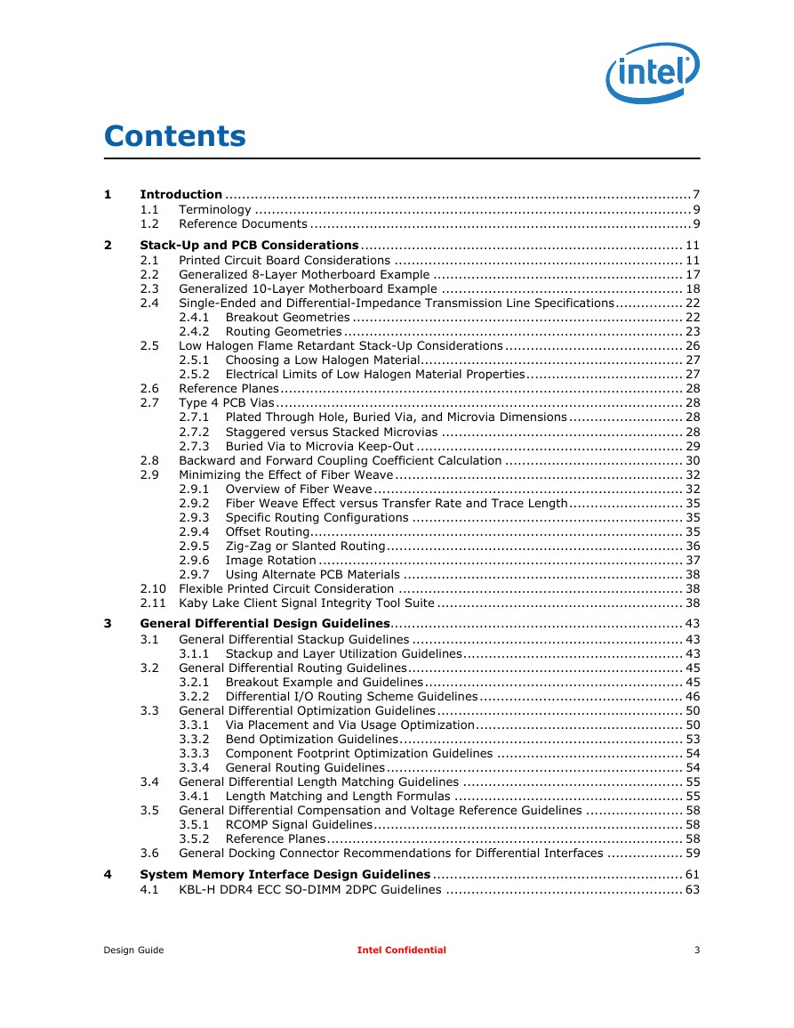
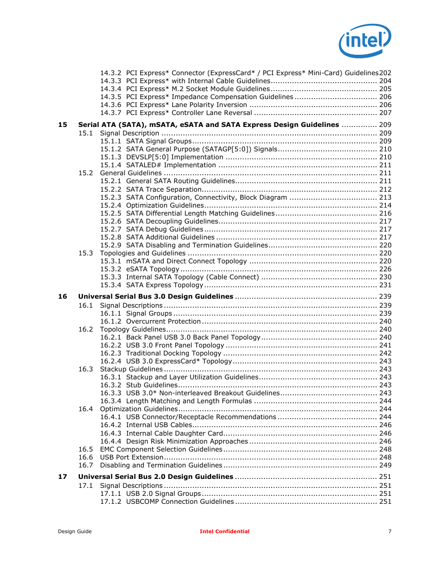
 Contents 1 2 3 4 2.5 3.2 3.3 2.8 2.9 2.6 2.7 Introduction ..............................................................................................................7 Terminology .......................................................................................................9 1.1 1.2 Reference Documents ..........................................................................................9 Stack-Up and PCB Considerations............................................................................ 11 Printed Circuit Board Considerations .................................................................... 11 2.1 Generalized 8-Layer Motherboard Example ........................................................... 17 2.2 Generalized 10-Layer Motherboard Example ......................................................... 18 2.3 2.4 Single-Ended and Differential-Impedance Transmission Line Specifications................ 22 2.4.1 Breakout Geometries .............................................................................. 22 2.4.2 Routing Geometries ................................................................................ 23 Low Halogen Flame Retardant Stack-Up Considerations .......................................... 26 2.5.1 Choosing a Low Halogen Material.............................................................. 27 2.5.2 Electrical Limits of Low Halogen Material Properties..................................... 27 Reference Planes............................................................................................... 28 Type 4 PCB Vias................................................................................................ 28 2.7.1 Plated Through Hole, Buried Via, and Microvia Dimensions ........................... 28 2.7.2 Staggered versus Stacked Microvias ......................................................... 28 2.7.3 Buried Via to Microvia Keep-Out ............................................................... 29 Backward and Forward Coupling Coefficient Calculation .......................................... 30 Minimizing the Effect of Fiber Weave.................................................................... 32 2.9.1 Overview of Fiber Weave......................................................................... 32 Fiber Weave Effect versus Transfer Rate and Trace Length........................... 35 2.9.2 2.9.3 Specific Routing Configurations ................................................................ 35 2.9.4 Offset Routing........................................................................................ 35 2.9.5 Zig-Zag or Slanted Routing...................................................................... 36 2.9.6 Image Rotation ...................................................................................... 37 2.9.7 Using Alternate PCB Materials .................................................................. 38 2.10 Flexible Printed Circuit Consideration ................................................................... 38 2.11 Kaby Lake Client Signal Integrity Tool Suite .......................................................... 38 General Differential Design Guidelines..................................................................... 43 General Differential Stackup Guidelines ................................................................ 43 3.1 3.1.1 Stackup and Layer Utilization Guidelines.................................................... 43 General Differential Routing Guidelines................................................................. 45 3.2.1 Breakout Example and Guidelines............................................................. 45 3.2.2 Differential I/O Routing Scheme Guidelines................................................ 46 General Differential Optimization Guidelines.......................................................... 50 3.3.1 Via Placement and Via Usage Optimization................................................. 50 3.3.2 Bend Optimization Guidelines................................................................... 53 3.3.3 Component Footprint Optimization Guidelines ............................................ 54 3.3.4 General Routing Guidelines...................................................................... 54 General Differential Length Matching Guidelines .................................................... 55 3.4.1 Length Matching and Length Formulas ...................................................... 55 General Differential Compensation and Voltage Reference Guidelines ....................... 58 3.5.1 RCOMP Signal Guidelines......................................................................... 58 3.5.2 Reference Planes.................................................................................... 58 3.6 General Docking Connector Recommendations for Differential Interfaces .................. 59 System Memory Interface Design Guidelines ........................................................... 61 4.1 KBL-H DDR4 ECC SO-DIMM 2DPC Guidelines ........................................................ 63 3.4 3.5 Design Guide Intel Confidential 3
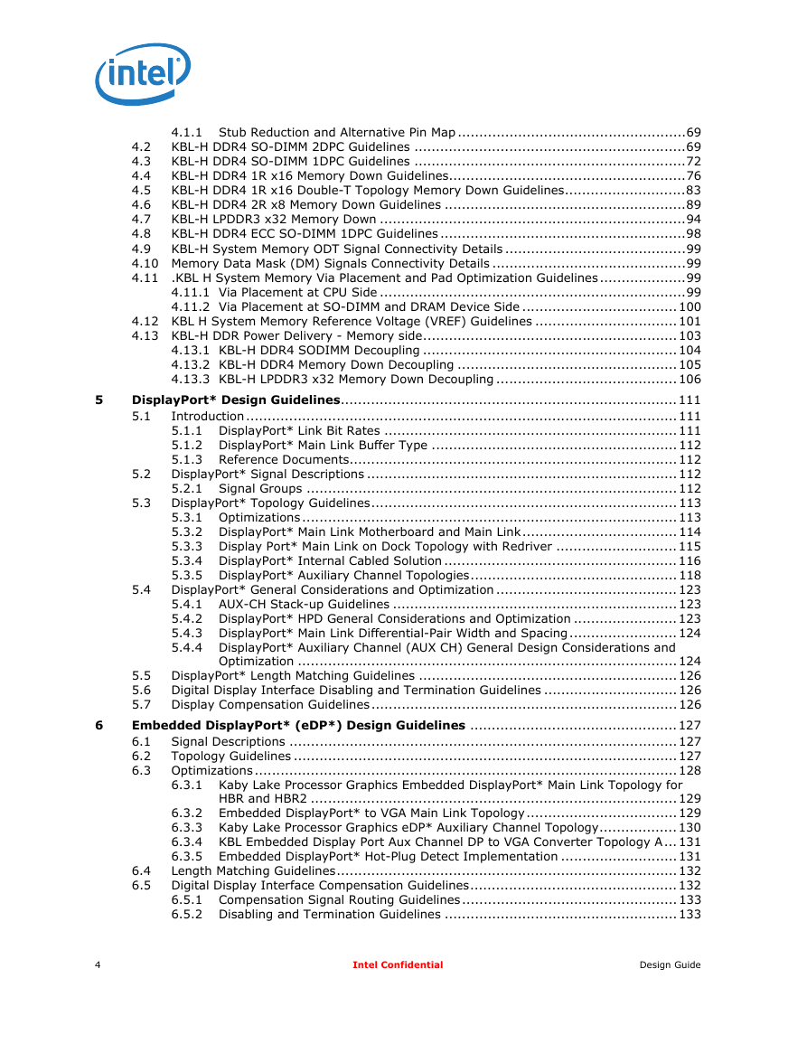
4.1.1 Stub Reduction and Alternative Pin Map .....................................................69 KBL-H DDR4 SO-DIMM 2DPC Guidelines ...............................................................69 4.2 KBL-H DDR4 SO-DIMM 1DPC Guidelines ...............................................................72 4.3 KBL-H DDR4 1R x16 Memory Down Guidelines.......................................................76 4.4 KBL-H DDR4 1R x16 Double-T Topology Memory Down Guidelines............................83 4.5 KBL-H DDR4 2R x8 Memory Down Guidelines ........................................................89 4.6 KBL-H LPDDR3 x32 Memory Down .......................................................................94 4.7 KBL-H DDR4 ECC SO-DIMM 1DPC Guidelines .........................................................98 4.8 4.9 KBL-H System Memory ODT Signal Connectivity Details ..........................................99 4.10 Memory Data Mask (DM) Signals Connectivity Details .............................................99 4.11 .KBL H System Memory Via Placement and Pad Optimization Guidelines ....................99 4.11.1 Via Placement at CPU Side .......................................................................99 4.11.2 Via Placement at SO-DIMM and DRAM Device Side .................................... 100 4.12 KBL H System Memory Reference Voltage (VREF) Guidelines ................................. 101 4.13 KBL-H DDR Power Delivery - Memory side........................................................... 103 4.13.1 KBL-H DDR4 SODIMM Decoupling ........................................................... 104 4.13.2 KBL-H DDR4 Memory Down Decoupling ...................................................105 4.13.3 KBL-H LPDDR3 x32 Memory Down Decoupling .......................................... 106 DisplayPort* Design Guidelines..............................................................................111 Introduction.................................................................................................... 111 5.1 5.1.1 DisplayPort* Link Bit Rates .................................................................... 111 5.1.2 DisplayPort* Main Link Buffer Type ......................................................... 112 5.1.3 Reference Documents............................................................................ 112 DisplayPort* Signal Descriptions ........................................................................ 112 5.2.1 Signal Groups ...................................................................................... 112 DisplayPort* Topology Guidelines....................................................................... 113 5.3.1 Optimizations ....................................................................................... 113 5.3.2 DisplayPort* Main Link Motherboard and Main Link.................................... 114 5.3.3 Display Port* Main Link on Dock Topology with Redriver ............................ 115 5.3.4 DisplayPort* Internal Cabled Solution ...................................................... 116 5.3.5 DisplayPort* Auxiliary Channel Topologies................................................ 118 DisplayPort* General Considerations and Optimization .......................................... 123 5.4.1 AUX-CH Stack-up Guidelines .................................................................. 123 5.4.2 DisplayPort* HPD General Considerations and Optimization ........................ 123 5.4.3 DisplayPort* Main Link Differential-Pair Width and Spacing......................... 124 5.4.4 DisplayPort* Auxiliary Channel (AUX CH) General Design Considerations and Optimization ........................................................................................ 124 5.5 DisplayPort* Length Matching Guidelines ............................................................ 126 5.6 Digital Display Interface Disabling and Termination Guidelines ............................... 126 5.7 Display Compensation Guidelines....................................................................... 126 Embedded DisplayPort* (eDP*) Design Guidelines ................................................127 Signal Descriptions .......................................................................................... 127 6.1 Topology Guidelines ......................................................................................... 127 6.2 6.3 Optimizations .................................................................................................. 128 6.3.1 Kaby Lake Processor Graphics Embedded DisplayPort* Main Link Topology for 5.4 5.2 5.3 HBR and HBR2 ..................................................................................... 129 6.3.2 Embedded DisplayPort* to VGA Main Link Topology................................... 129 6.3.3 Kaby Lake Processor Graphics eDP* Auxiliary Channel Topology.................. 130 6.3.4 KBL Embedded Display Port Aux Channel DP to VGA Converter Topology A... 131 6.3.5 Embedded DisplayPort* Hot-Plug Detect Implementation ........................... 131 Length Matching Guidelines............................................................................... 132 Digital Display Interface Compensation Guidelines................................................ 132 6.5.1 Compensation Signal Routing Guidelines.................................................. 133 6.5.2 Disabling and Termination Guidelines ...................................................... 133 6.4 6.5 Intel Confidential Design Guide 5 6 4
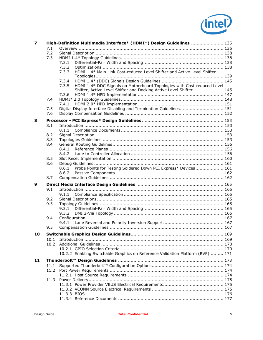
 7 8 9 10 11 7.4 8.5 8.6 9.4 High-Definition Multimedia Interface* (HDMI*) Design Guidelines ....................... 135 Overview ....................................................................................................... 135 7.1 Signal Description ........................................................................................... 138 7.2 7.3 HDMI 1.4* Topology Guidelines......................................................................... 138 7.3.1 Differential-Pair Width and Spacing......................................................... 138 7.3.2 Optimizations ...................................................................................... 138 7.3.3 HDMI 1.4* Main Link Cost-reduced Level Shifter and Active Level Shifter Topologies........................................................................................... 139 7.3.4 HDMI 1.4* (DDC) Signals Design Guidelines ............................................ 145 7.3.5 HDMI 1.4* DDC Signals on Motherboard Topologies with Cost-reduced Level 8.2 8.3 8.4 Shifter, Active Level Shifter and Docking Active Level Shifter...................... 145 7.3.6 HDMI 1.4* HPD Implementation............................................................. 147 HDMI* 2.0 Topology Guidelines......................................................................... 148 7.4.1 HDMI 2.0* HPD Implementation............................................................. 151 Digital Display Interface Disabling and Termination Guidelines............................... 151 7.5 7.6 Display Compensation Guidelines ...................................................................... 152 Processor - PCI Express* Design Guidelines .......................................................... 153 Introduction ................................................................................................... 153 8.1 8.1.1 Compliance Documents ......................................................................... 153 Signal Description ........................................................................................... 153 Topologies Guidelines ...................................................................................... 153 General Routing Guidelines............................................................................... 156 8.4.1 Reference Planes.................................................................................. 156 8.4.2 Lane to Controller Allocation .................................................................. 156 Slot Reset Implementation ............................................................................... 160 Debug Guidelines ............................................................................................ 161 Probe Points for Testing Soldered Down PCI Express* Devices.................... 161 8.6.1 8.6.2 Passive Components ............................................................................. 162 8.7 Compensation Guidelines ................................................................................. 162 Direct Media Interface Design Guidelines .............................................................. 165 Introduction ................................................................................................... 165 9.1 9.1.1 Compliance Specification ....................................................................... 165 Signal Descriptions .......................................................................................... 165 Topology Guidelines......................................................................................... 165 9.3.1 Differential-Pair Width and Spacing......................................................... 165 9.3.2 DMI 2-Via Topology .............................................................................. 165 Configuration.................................................................................................. 167 9.4.1 Lane Reversal and Polarity Inversion Support........................................... 167 Compensation Guidelines ................................................................................. 167 9.5 Switchable Graphics Design Guidelines.................................................................. 169 10.1 Introduction ................................................................................................... 169 10.2 Additional Guidelines ....................................................................................... 170 10.2.1 GPIO Selection Criteria.......................................................................... 170 10.2.2 Enabling Switchable Graphics on Reference Validation Platform (RVP).......... 171 Thunderbolt™ Design Guidelines ........................................................................... 173 11.1 Supported Thunderbolt™ Configuration Options................................................... 174 11.2 Port Power Requirements ................................................................................. 174 11.2.1 Host Source Requirements .................................................................... 174 11.3 Power Delivery................................................................................................ 175 11.3.1 Power Provider VBUS Electrical Requirements........................................... 175 11.3.2 VCONN Source Electrical Requirements ................................................... 175 11.3.3 BIOS .................................................................................................. 176 11.3.4 Reference Documents ........................................................................... 177 9.2 9.3 Design Guide Intel Confidential 5
11.3.5 Compliance Specification ....................................................................... 177 11.3.6 Signal Descriptions ............................................................................... 178 11.4 Topology Guidelines ......................................................................................... 178 11.4.1 Motherboard Down Topology .................................................................. 178 11.4.2 DisplayPort* to Thunderbolt™ Topology ...................................................179 11.4.3 Add-In Card Topology ........................................................................... 180 11.4.4 Connector Guideline .............................................................................. 181 11.5 Length Matching Guidelines............................................................................... 181 11.6 Stack-up Guidelines ......................................................................................... 182 11.6.1 Stack-up and Layer Utilization Guidelines ................................................. 182 11.6.2 Thunderbolt™ Insertion Loss Spec .......................................................... 183 11.7 Optimization Guidelines .................................................................................... 183 11.7.1 TBT Lane Routing and Component Placement ........................................... 183 11.7.2 Via Placement and Via Pad Optimization...................................................183 11.8 Debug Guidelines............................................................................................. 183 11.8.1 PCIe* and DisplayPort* Configuration...................................................... 183 11.8.2 NVM Configuration ................................................................................ 184 11.9 Additional Guidelines........................................................................................ 184 11.9.1 Crystal Design Requirement ................................................................... 184 11.9.2 NVM.................................................................................................... 184 Asynchronous and Sideband Signals Design Guidelines..........................................185 12.1 Signal Descriptions .......................................................................................... 185 12.1.1 Signal Groups ...................................................................................... 185 12.2 Topology Guidelines ......................................................................................... 186 12.2.1 PROCHOT# Topology ............................................................................ 187 12.2.2 CATERR# Topology ............................................................................... 188 12.2.3 PROCPWRGD Topology .......................................................................... 189 12.2.4 VCCST_PWRGOOD Topology .................................................................. 189 12.2.5 THERMTRIP# Topology .......................................................................... 190 12.2.6 RESET# (PLTRST#) Topology ................................................................. 191 12.2.7 Platform Environmental Control Interface (PECI) Topology ......................... 191 12.2.8 BPM#[3:0] Topology ............................................................................. 193 12.2.9 PM_SYNC Topology ............................................................................... 193 12.2.10PM_DOWN Topology.............................................................................. 194 12.2.11PROC_TRIGIN Topology (PCH to Processor_TRIGIN) .................................. 194 12.2.12PROC_TRIGOUT Topology (Processor to PCH_TRIGIN) ............................... 195 12.2.13SVID Topology ..................................................................................... 195 12.2.14COMP Signals....................................................................................... 196 12.3 ESD Protection for Asynchronous Signals ............................................................ 196 Flexible I/O ...........................................................................................................197 13.1 Introduction.................................................................................................... 197 13.2 Flexible I/O Implementation.............................................................................. 197 13.2.1 U Kaby Lake PCH-H.............................................................................. 197 13.3 HSIO Lane Selection ........................................................................................ 198 13.3.1 PCIe*/SATA Lane Selection .................................................................... 198 13.4 HSIO Board Routing ......................................................................................... 198 PCI Express* Interface Design Guidelines..............................................................199 14.1 Introduction.................................................................................................... 199 14.1.1 Intel® Rapid Storage Technology (Intel® RST) for PCIe* Storage ................ 200 14.2 PCI Express* Guideline Terminology and Descriptions........................................... 200 14.2.1 PCI Express* Signal Descriptions ............................................................ 200 14.3 PCI Express* Routing Guidelines........................................................................ 201 14.3.1 PCI Express* Device Down Guidelines ..................................................... 201 Intel Confidential Design Guide 12 13 14 6
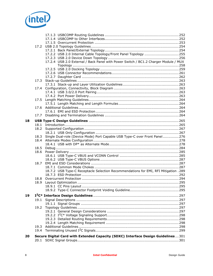
 15 16 17 14.3.2 PCI Express* Connector (ExpressCard* / PCI Express* Mini-Card) Guidelines202 14.3.3 PCI Express* with Internal Cable Guidelines............................................. 204 14.3.4 PCI Express* M.2 Socket Module Guidelines............................................. 205 14.3.5 PCI Express* Impedance Compensation Guidelines ................................... 206 14.3.6 PCI Express* Lane Polarity Inversion ...................................................... 206 14.3.7 PCI Express* Controller Lane Reversal .................................................... 207 Serial ATA (SATA), mSATA, eSATA and SATA Express Design Guidelines ............... 209 15.1 Signal Description ........................................................................................... 209 15.1.1 SATA Signal Groups.............................................................................. 209 15.1.2 SATA General Purpose (SATAGP[5:0]) Signals.......................................... 210 15.1.3 DEVSLP[5:0] Implementation ................................................................ 210 15.1.4 SATALED# Implementation ................................................................... 211 15.2 General Guidelines .......................................................................................... 211 15.2.1 General SATA Routing Guidelines............................................................ 211 15.2.2 SATA Trace Separation.......................................................................... 212 15.2.3 SATA Configuration, Connectivity, Block Diagram ..................................... 213 15.2.4 Optimization Guidelines......................................................................... 214 15.2.5 SATA Differential Length Matching Guidelines........................................... 216 15.2.6 SATA Decoupling Guidelines................................................................... 217 15.2.7 SATA Debug Guidelines......................................................................... 217 15.2.8 SATA Additional Guidelines .................................................................... 217 15.2.9 SATA Disabling and Termination Guidelines.............................................. 220 15.3 Topologies and Guidelines ................................................................................ 220 15.3.1 mSATA and Direct Connect Topology ...................................................... 220 15.3.2 eSATA Topology ................................................................................... 226 15.3.3 Internal SATA Topology (Cable Connect) ................................................. 230 15.3.4 SATA Express Topology......................................................................... 231 Universal Serial Bus 3.0 Design Guidelines ............................................................ 239 16.1 Signal Descriptions .......................................................................................... 239 16.1.1 Signal Groups ...................................................................................... 239 16.1.2 Overcurrent Protection.......................................................................... 240 16.2 Topology Guidelines......................................................................................... 240 16.2.1 Back Panel USB 3.0 Back Panel Topology................................................. 240 16.2.2 USB 3.0 Front Panel Topology ................................................................ 241 16.2.3 Traditional Docking Topology ................................................................. 242 16.2.4 USB 3.0 ExpressCard* Topology............................................................. 243 16.3 Stackup Guidelines .......................................................................................... 243 16.3.1 Stackup and Layer Utilization Guidelines.................................................. 243 16.3.2 Stub Guidelines.................................................................................... 243 16.3.3 USB 3.0* Non-interleaved Breakout Guidelines......................................... 243 16.3.4 Length Matching and Length Formulas .................................................... 244 16.4 Optimization Guidelines.................................................................................... 244 16.4.1 USB Connector/Receptacle Recommendations .......................................... 244 16.4.2 Internal USB Cables.............................................................................. 246 16.4.3 Internal Cable Daughter Card................................................................. 246 16.4.4 Design Risk Minimization Approaches ...................................................... 246 16.5 EMC Component Selection Guidelines................................................................. 248 16.6 USB Port Extension.......................................................................................... 248 16.7 Disabling and Termination Guidelines ................................................................. 249 Universal Serial Bus 2.0 Design Guidelines ............................................................ 251 17.1 Signal Descriptions .......................................................................................... 251 17.1.1 USB 2.0 Signal Groups.......................................................................... 251 17.1.2 USBCOMP Connection Guidelines ............................................................ 251 Design Guide Intel Confidential 7
17.1.3 USBCOMP Routing Guidelines ................................................................. 252 17.1.4 USBCOMP to Other Interfaces................................................................. 252 17.1.5 Overcurrent Protection .......................................................................... 253 17.2 USB 2.0 Topology Guidelines............................................................................. 254 17.2.1 Back Panel/External Topology................................................................. 254 17.2.2 USB 2.0 Internal Cable Topology/Front Panel Topology .............................. 255 17.2.3 USB 2.0 Device Down Topology .............................................................. 256 17.2.4 USB 2.0 External / Back Panel with Power Switch / BC1.2 Charger Module / MUX Topology ............................................................................................. 258 17.2.5 USB 2.0 Docking Topology ..................................................................... 259 17.2.6 USB Connector Recommendations........................................................... 261 17.2.7 Daughter Card ..................................................................................... 262 17.3 Stack-up Guidelines ......................................................................................... 263 17.3.1 Stack-up and Layer Utilization Guidelines ................................................. 263 17.4 Configuration, Connectivity, Block Diagram ......................................................... 263 17.4.1 USB 3.0/2.0 Port Pairing........................................................................ 263 17.4.2 Port Power Delivery............................................................................... 263 17.5 Length Matching Guidelines............................................................................... 264 17.5.1 Length Matching and Length Formulas..................................................... 264 17.6 Additional Guidelines........................................................................................ 264 17.6.1 EMI and ESD Protection ......................................................................... 264 17.7 Disabling and Termination Guidelines ................................................................. 264 USB Type-C Design Guidelines ...............................................................................265 18.1 Introduction.................................................................................................... 265 18.2 Supported Configuration ................................................................................... 267 18.2.1 USB Only Configuration ......................................................................... 267 18.3 Single Dual-role (Device Mode) Port Capable USB Type-C over Front Panel .............. 276 18.4 Alternate Modes Configuration ........................................................................... 278 18.4.1 USB with DP* as Alternate Mode............................................................. 278 18.5 Debug............................................................................................................ 284 18.6 Power Delivery ................................................................................................ 285 18.6.1 USB Type-C VBUS and VCONN Control .................................................... 285 18.6.2 USB Type-C VBUS Options ..................................................................... 287 18.7 EMI and ESD Considerations ............................................................................. 287 18.7.1 Common Mode Chokes .......................................................................... 287 18.7.2 USB Type-C Receptacle Selection Recommendations for EMI, RFI Mitigation . 289 18.7.3 ESD Protection ..................................................................................... 292 18.8 Overcurrent Protection ..................................................................................... 294 18.9 Layout Optimization ......................................................................................... 295 18.9.1 CC Pins Layout ..................................................................................... 295 18.9.2 Type-C Connector Footprint Voiding Guideline........................................... 295 I2C* Interface Design Guidelines ........................................................................... 297 19.1 Signal Descriptions .......................................................................................... 297 19.1.1 Signal Groups ...................................................................................... 297 19.2 Topology Guidelines ......................................................................................... 297 19.2.1 General Design Considerations ............................................................... 297 19.2.2 I2C* Voltage Signaling Support............................................................... 298 19.2.3 Detailed Routing Requirements............................................................... 298 19.2.4 Length Matching Requirement ................................................................ 298 19.3 Additional Guidelines........................................................................................ 298 19.4 Terminating Unused I2C Signals......................................................................... 299 Secure Digital Card with Extended Capacity (SDXC) Interface Design Guidelines ... 301 20.1 SDXC Signal Groups.........................................................................................301 Intel Confidential Design Guide 18 19 20 8
分享到:
收藏