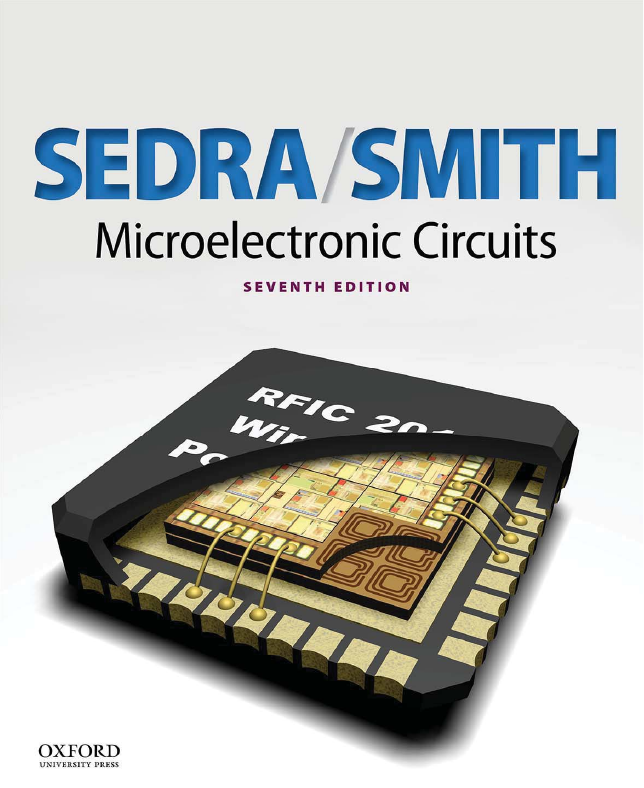
MICROELECTRONIC CIRCUITS; 7E
Series Page
Title Page
Copyright
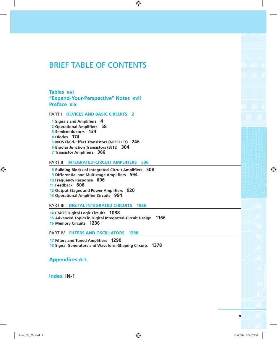
Brief Table of Contents
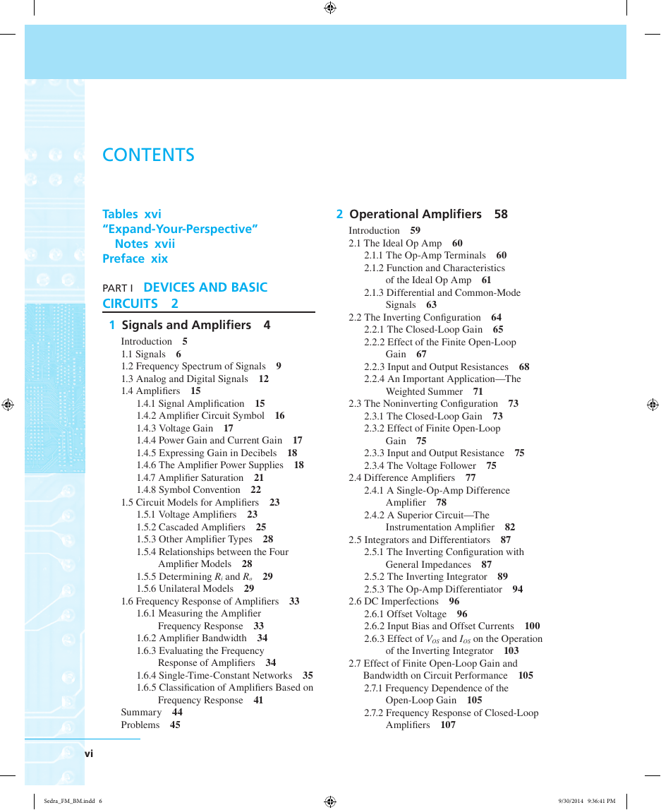
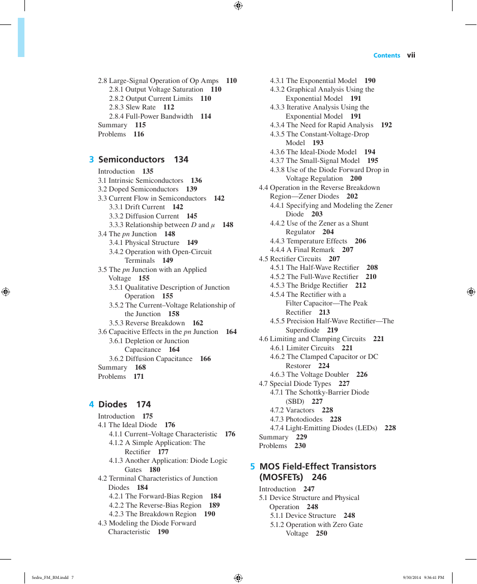
Contents
Tables
“Expand-Your-Perspective” Notes
Preface
Prerequisites
Emphasis on Design
New to the Seventh Edition
The Book’s Website
Exercises and End-of-Chapter Problems
Course Organization
The First Course
The Second Course
A Digitally Oriented First Course
Supplemental Material/Third Course
The Accompanying Laboratory
An Outline for the Reader
Ancillaries
For the Instructor
For the Student and Instructor
Acknowledgments
Reviewers of Seventh Edition
Reviewers of Prior Editions
PART I - DEVICES AND BASIC CIRCUITS
Chapter 1 - Signals and Amplifiers
Introduction
1.1 Signals
1.2 Frequency Spectrum of Signals
1.3 Analog and Digital Signals
1.4 Amplifiers
1.4.1 Signal Amplification
1.4.2 Amplifier Circuit Symbol
1.4.3 Voltage Gain
1.4.4 Power Gain and Current Gain
1.4.5 Expressing Gain in Decibels
1.4.6 The Amplifier Power Supplies
1.4.7 Amplifier Saturation
1.4.8 Symbol Convention
1.5 Circuit Models for Amplifiers
1.5.1 Voltage Amplifiers
1.5.2 Cascaded Amplifiers
1.5.3 Other Amplifier Types
1.5.4 Relationships between the Four Amplifier Models
1.5.5 Determining R_i and R_o
1.5.6 Unilateral Models
1.6 Frequency Response of Amplifiers
1.6.1 Measuring the Amplifier Frequency Response
1.6.2 Amplifier Bandwidth
1.6.3 Evaluating the Frequency Response of Amplifiers
1.6.4 Single-Time-Constant Networks
1.6.5 Classification of Amplifiers Based on Frequency Response
Summary
Problems
Chapter 2 - Operational Amplifiers
Introduction
2.1 The Ideal Op Amp
2.1.1 The Op-Amp Terminals
2.1.2 Function and Characteristics of the Ideal Op Amp
2.1.3 Differential and Common-Mode Signals
2.2 The Inverting Configuration
2.2.1 The Closed-Loop Gain
2.2.2 Effect of the Finite Open-Loop Gain
2.2.3 Input and Output Resistances
2.2.4 An Important Application—The Weighted Summer
2.3 The Noninverting Configuration
2.3.1 The Closed-Loop Gain
2.3.2 Effect of Finite Open-Loop Gain
2.3.3 Input and Output Resistance
2.3.4 The Voltage Follower
2.4 Difference Amplifiers
2.4.1 A Single-Op-Amp Difference Amplifier
2.4.2 A Superior Circuit—The Instrumentation Amplifier
2.5 Integrators and Differentiators
2.5.1 The Inverting Configuration with General Impedances
2.5.2 The Inverting Integrator
2.5.3 The Op-Amp Differentiator
2.6 DC Imperfections
2.6.1 Offset Voltage
2.6.2 Input Bias and Offset Currents
2.6.3 Effect of V_OS and I_OS on the Operation of the Inverting Integrator
2.7 Effect of Finite Open-Loop Gain and Bandwidth on Circuit Performance
2.7.1 Frequency Dependence of the Open-Loop Gain
2.7.2 Frequency Response of Closed-Loop Amplifiers
2.8 Large-Signal Operation of Op Amps
2.8.1 Output Voltage Saturation
2.8.2 Output Current Limits
2.8.3 Slew Rate
2.8.4 Full-Power Bandwidth
Summary
Problems
Chapter 3 - Semiconductors
Introduction
3.1 Intrinsic Semiconductors
3.2 Doped Semiconductors
3.3 Current Flow in Semiconductors
3.3.1 Drift Current
3.3.2 Diffusion Current
3.3.3 Relationship between D and μ
3.4 The pn Junction
3.4.1 Physical Structure
3.4.2 Operation with Open-Circuit Terminals
3.5 The pn Junction with an Applied Voltage
3.5.1 Qualitative Description of Junction Operation
3.5.2 The Current–Voltage Relationship of the Junction
3.5.3 Reverse Breakdown
3.6 Capacitive Effects in the pn Junction
3.6.1 Depletion or Junction Capacitance
3.6.2 Diffusion Capacitance
Summary
Problems
Chapter 4 - Diodes
Introduction
4.1 The Ideal Diode
4.1.1 Current–Voltage Characteristic
4.1.2 A Simple Application: The Rectifier
4.1.3 Another Application: Diode Logic Gates
4.2 Terminal Characteristics of Junction Diodes
4.2.1 The Forward-Bias Region
4.2.2 The Reverse-Bias Region
4.2.3 The Breakdown Region
4.3 Modeling the Diode Forward Characteristic
4.3.1 The Exponential Model
4.3.2 Graphical Analysis Using the Exponential Model
4.3.3 Iterative Analysis Using the Exponential Model
4.3.4 The Need for Rapid Analysis
4.3.5 The Constant-Voltage-Drop Model
4.3.6 The Ideal-Diode Model
4.3.7 The Small-Signal Model
4.3.8 Use of the Diode Forward Drop in Voltage Regulation
4.4 Operation in the Reverse Breakdown Region—Zener Diodes
4.4.1 Specifying and Modeling the Zener Diode
4.4.2 Use of the Zener as a Shunt Regulator
4.4.3 Temperature Effects
4.4.4 A Final Remark
4.5 Rectifier Circuits
4.5.1 The Half-Wave Rectifier
4.5.2 The Full-Wave Rectifier
4.5.3 The Bridge Rectifier
4.5.4 The Rectifier with a Filter Capacitor—The Peak Rectifier
4.5.5 Precision Half-Wave Rectifier—The Superdiode
4.6 Limiting and Clamping Circuits
4.6.1 Limiter Circuits
4.6.2 The Clamped Capacitor or DC Restorer
4.6.3 The Voltage Doubler
4.7 Special Diode Types
4.7.1 The Schottky-Barrier Diode (SBD)
4.7.2 Varactors
4.7.3 Photodiodes
4.7.4 Light-Emitting Diodes (LEDs)
Summary
Problems
Chapter 5 - MOS Field-Effect Transistors (MOSFETs)
Introduction
5.1 Device Structure and Physical Operation
5.1.1 Device Structure
5.1.2 Operation with Zero Gate Voltage
5.1.3 Creating a Channel for Current Flow
5.1.4 Applying a Small v_DS
5.1.5 Operation as v DS Is Increased
5.1.6 Operation for v_DS ≥ V_OV: Channel Pinch-Off and Current Saturation
5.1.7 The p-Channel MOSFET
5.1.8 Complementary MOS or CMOS
5.1.9 Operating the MOS Transistor in the Subthreshold Region
5.2 Current–Voltage Characteristics
5.2.1 Circuit Symbol
5.2.2 The i_D–v_DS Characteristics
5.2.3 The i_D–v_GS Characteristic
5.2.4 Finite Output Resistance in Saturation
5.2.5 Characteristics of the p-Channel MOSFET
5.3 MOSFET Circuits at DC
5.4 The Body Effect and Other Topics
5.4.1 The Role of the Substrate—The Body Effect
5.4.2 Temperature Effects
5.4.3 Breakdown and Input Protection
5.4.4 Velocity Saturation
5.4.5 The Depletion-Type MOSFET
Summary
Problems
Chapter 6 - Bipolar Junction Transistors (BJTs)
Introduction
6.1 Device Structure and Physical Operation
6.1.1 Simplified Structure and Modes of Operation
6.1.2 Operation of the npn Transistor in the Active Mode
6.1.3 Structure of Actual Transistors
6.1.4 Operation in the Saturation Mode
6.1.5 The pnp Transistor
6.2 Current–Voltage Characteristics
6.2.1 Circuit Symbols and Conventions
6.2.2 Graphical Representation of Transistor Characteristics
6.2.3 Dependence of i_C on the Collector Voltage—The Early Effect
6.2.4 An Alternative Form of the Common-Emitter Characteristics
6.3 BJT Circuits at DC
6.4 Transistor Breakdown and Temperature Effects
6.4.1 Transistor Breakdown
6.4.2 Dependence of β on I_C and Temperature
Summary
Problems
Chapter 7 - Transistor Amplifiers
Introduction
7.1 Basic Principles
7.1.1 The Basis for Amplifier Operation
7.1.2 Obtaining a Voltage Amplifier
7.1.3 The Voltage-Transfer Characteristic (VTC)
7.1.4 Obtaining Linear Amplification by Biasing the Transistor
7.1.5 The Small-Signal Voltage Gain
7.1.6 Determining the VTC by Graphical Analysis
7.1.7 Deciding on a Location for the Bias Point Q
7.2 Small-Signal Operation and Models
7.2.1 The MOSFET Case
7.2.2 The BJT Case
7.2.3 Summary Tables
7.3 Basic Configurations
7.3.1 The Three Basic Configurations
7.3.2 Characterizing Amplifiers
7.3.3 The Common-Source (CS) and Common-Emitter (CE) Amplifiers
7.3.4 The Common-Source (Common-Emitter) Amplifier with a Source (Emitter) Resistance
7.3.5 The Common-Gate (CG) and the Common-Base (CB) Amplifiers
7.3.6 The Source and Emitter Followers
7.3.7 Summary Tables and Comparisons
7.3.8 When and How to Include the Transistor Output Resistance r_o
7.4 Biasing
7.4.1 The MOSFET Case
7.4.2 The BJT Case
7.5 Discrete-Circuit Amplifiers
7.5.1 A Common-Source (CS) Amplifier
7.5.2 A Common-Emitter (CE) Amplifier
7.5.3 A Common-Emitter Amplifier with an Emitter Resistance R_e
7.5.4 A Common-Base (CB) Amplifier
7.5.5 An Emitter Follower
7.5.6 The Amplifier Frequency Response
Summary
Problems
PART II - INTEGRATED-CIRCUIT AMPLIFIERS
Chapter 8 - Building Blocks of Integrated-Circuit Amplifiers
Introduction
8.1 IC Design Philosophy
8.2 IC Biasing—Current Sources, Current Mirrors, and Current-Steering Circuits
8.2.1 The Basic MOSFET Current Source
8.2.2 MOS Current-Steering Circuits
8.2.3 BJT Circuits
8.2.4 Small-Signal Operation of Current Mirrors
8.3 The Basic Gain Cell
8.3.1 The CS and CE Amplifiers with Current-Source Loads
8.3.2 The Intrinsic Gain
8.3.3 Effect of the Output Resistance of the Current-Source Load
8.3.4 Increasing the Gain of the Basic Cell
8.4 The Common-Gate and Common-Base Amplifiers
8.4.1 The CG Circuit
8.4.2 Output Resistance of a CS Amplifier with a Source Resistance
8.4.3 The Body Effect
8.4.4 The CB Circuit
8.4.5 Output Resistance of an Emitter-Degenerated CE Amplifier
8.5 The Cascode Amplifier
8.5.1 Cascoding
8.5.2 The MOS Cascode Amplifier
8.5.3 Distribution of Voltage Gain in a Cascode Amplifier
8.5.4 Double Cascoding
8.5.5 The Folded Cascode
8.5.6 The BJT Cascode
8.6 Current-Mirror Circuits with Improved Performance
8.6.1 Cascode MOS Mirrors
8.6.2 The Wilson Current Mirror
8.6.3 The Wilson MOS Mirror
8.6.4 The Widlar Current Souce
8.7 Some Useful Transistor Pairings
8.7.1 The CC–CE, CD–CS, and CD–CE Configurations
8.7.2 The Darlington Configuration
8.7.3 The CC–CB and CD–CG Configurations
Summary
Problems
Chapter 9 - Differential and Multistage Amplifiers
Introduction
9.1 The MOS Differential Pair
9.1.1 Operation with a Common-Mode Input Voltage
9.1.2 Operation with a Differential Input Voltage
9.1.3 Large-Signal Operation
9.1.4 Small-Signal Operation
9.1.5 The Differential Amplifier with Current-Source Loads
9.1.6 Cascode Differential Amplifier
9.2 The BJT Differential Pair
9.2.1 Basic Operation
9.2.2 Input Common-Mode Range
9.2.3 Large-Signal Operation
9.2.4 Small-Signal Operation
9.3 Common-Mode Rejection
9.3.1 The MOS Case
9.3.2 The BJT Case
9.4 DC Offset
9.4.1 Input Offset Voltage of the MOS Differential Amplifier
9.4.2 Input Offset Voltage of the Bipolar Differential Amplifier
9.4.3 Input Bias and Offset Currents of the Bipolar Differential Amplifier
9.4.4 A Concluding Remark
9.5 The Differential Amplifier with a Current-Mirror Load
9.5.1 Differential to Single-Ended Conversion
9.5.2 The Current-Mirror-Loaded MOS Differential Pair
9.5.3 Differential Gain of the Current-Mirror-Loaded MOS Pair
9.5.4 The Bipolar Differential Pair with a Current-Mirror Load
9.5.5 Common-Mode Gain and CMRR
9.6 Multistage Amplifiers
9.6.1 A Two-Stage CMOS Op Amp
9.6.2 A Bipolar Op Amp
Summary
Problems
Chapter 10 - Frequency Response
Introduction
10.1 Low-Frequency Response of Discrete-Circuit Common-Source and Common-Emitter Amplifiers
10.1.1 The CS Amplifier
10.1.2 The Method of Short-Circuit Time-Constants
10.1.3 The CE Amplifier
10.2 Internal Capacitive Effects and the High-Frequency Model of the MOSFET and the BJT
10.2.1 The MOSFET
10.2.2 The BJT
10.3 High-Frequency Response of the CS and CE Amplifiers
10.3.1 The Common-Source Amplifier
10.3.2 The Common-Emitter Amplifier
10.3.3 Miller’s Theorem
10.3.4 Frequency Response of the CS Amplifier When R_sig Is Low
10.4 Useful Tools for the Analysis of the High-Frequency Response of Amplifiers
10.4.1 The High-Frequency Gain Function
10.4.2 Determining the 3-dB Frequency f_H
10.4.3 The Method of Open-Circuit Time Constants
10.4.4 Application of the Method of Open-Circuit Time Constants to the CS Amplifier
10.4.5 Application of the Method of Open-Circuit Time Constants to the CE Amplifier
10.5 High-Frequency Response of the Common-Gate and Cascode Amplifiers
10.5.1 High-Frequency Response of the CG Amplifier
10.5.2 High-Frequency Response of the MOS Cascode Amplifier
10.5.3 High-Frequency Response of the Bipolar Cascode Amplifier
10.6 High-Frequency Response of the Source and Emitter Followers
10.6.1 The Source-Follower Case
10.6.2 The Emitter-Follower Case
10.7 High-Frequency Response of Differential Amplifiers
10.7.1 Analysis of the Resistively Loaded MOS Amplifier
10.7.2 Analysis of the Current-Mirror-Loaded MOS Amplifier
10.8 Other Wideband Amplifier Configurations
10.8.1 Obtaining Wideband Amplification by Source and Emitter Degeneration
10.8.2 The CD–CS, CC–CE, and CD–CE Configurations
10.8.3 The CC–CB and CD–CG Configurations
Summary
Problems
Chapter 11 - Feedback
Introduction
11.1 The General Feedback Structure
11.1.1 Signal-Flow Diagram
11.1.2 The Closed-Loop Gain
11.1.3 The Loop Gain
11.1.4 Summary
11.2 Some Properties of Negative Feedback
11.2.1 Gain Desensitivity
11.2.2 Bandwidth Extension
11.2.3 Interference Reduction
11.2.4 Reduction in Nonlinear Distortion
11.3 The Feedback Voltage Amplifier
11.3.1 The Series–Shunt Feedback Topology
11.3.2 Examples of Series–Shunt Feedback Amplifiers
11.3.3 Analysis of the Feedback Voltage Amplifier Utilizing the Loop Gain
11.3.4 A Final Remark
11.4 Systematic Analysis of Feedback Voltage Amplifiers
11.4.1 The Ideal Case
11.4.2 The Practical Case
11.5 Other Feedback Amplifier Types
11.5.1 Basic Principles
11.5.2 The Feedback Transconductance Amplifier (Series–Series)
11.5.3 The Feedback Transresistance Amplifier (Shunt–Shunt)
11.5.4 The Feedback Current Amplifier (Shunt–Series)
11.6 Summary of the Feedback Analysis Method
11.7 The Stability Problem
11.7.1 Transfer Function of the Feedback Amplifier
11.7.2 The Nyquist Plot
11.8 Effect of Feedback on the Amplifier Poles
11.8.1 Stability and Pole Location
11.8.2 Poles of the Feedback Amplifier
11.8.3 Amplifier with a Single-Pole Response
11.8.4 Amplifier with a Two-Pole Response
11.8.5 Amplifiers with Three or More Poles
11.9 Stability Study Using Bode Plots
11.9.1 Gain and Phase Margins
11.9.2 Effect of Phase Margin on Closed-Loop Response
11.9.3 An Alternative Approach for Investigating Stability
11.10 Frequency Compensation
11.10.1 Theory
11.10.2 Implementation
11.10.3 Miller Compensation and Pole Splitting
Summary
Problems
Chapter 12 - Output Stages and Power Amplifiers
Introduction
12.1 Classification of Output Stages
12.2 Class A Output Stage
12.2.1 Transfer Characteristic
12.2.2 Signal Waveforms
12.2.3 Power Dissipation
12.2.4 Power-Conversion Efficiency
12.3 Class B Output Stage
12.3.1 Circuit Operation
12.3.2 Transfer Characteristic
12.3.3 Power-Conversion Efficiency
12.3.4 Power Dissipation
12.3.5 Reducing Crossover Distortion
12.3.6 Single-Supply Operation
12.4 Class AB Output Stage
12.4.1 Circuit Operation
12.4.2 Output Resistance
12.5 Biasing the Class AB Circuit
12.5.1 Biasing Using Diodes
12.5.2 Biasing Using the V BE Multiplier
12.6 Variations on the Class AB Configuration
12.6.1 Use of Input Emitter Followers
12.6.2 Use of Compound Devices
12.6.3 Short-Circuit Protection
12.6.4 Thermal Shutdown
12.7 CMOS Class AB Output Stages
12.7.1 The Classical Configuration
12.7.2 An Alternative Circuit Utilizing Common-Source Transistors
12.8 IC Power Amplifiers
12.8.1 A Fixed-Gain IC Power Amplifier
12.8.2 The Bridge Amplifier
12.9 Class D Power Amplifiers
12.10 Power Transistors
12.10.1 Packages and Heat Sinks
12.10.2 Power BJTs
12.10.3 Power MOSFETs
12.10.4 Thermal Considerations
Summary
Problems
Chapter 13 - Operational-Amplifier Circuits
Introduction
13.1 The Two-Stage CMOS Op Amp
13.1.1 The Circuit
13.1.2 Input Common-Mode Range and Output Swing
13.1.3 DC Voltage Gain
13.1.4 Common-Mode Rejection Ratio (CMRR)
13.1.5 Frequency Response
13.1.6 Slew Rate
13.1.7 Power-Supply Rejection Ratio (PSRR)
13.1.8 Design Trade-Offs
13.1.9 A Bias Circuit for the Two-Stage CMOS Op Amp
13.2 The Folded-Cascode CMOS Op Amp
13.2.1 The Circuit
13.2.2 Input Common-Mode Range and Output Swing
13.2.3 Voltage Gain
13.2.4 Frequency Response
13.2.5 Slew Rate
13.2.6 Increasing the Input Common-Mode Range: Rail-to-Rail Input Operation
13.2.7 Increasing the Output Voltage Range: The Wide-Swing Current Mirror
13.3 The 741 BJT Op Amp
13.3.1 The 741 Circuit
13.3.2 DC Analysis
13.3.3 Small-Signal Analysis
13.3.4 Frequency Response
13.3.5 Slew Rate
13.4 Modern Techniques for the Design of BJT Op Amps
13.4.1 Special Performance Requirements
13.4.2 Bias Design
13.4.3 Design of the Input Stage to Obtain Rail-to-Rail V ICM
13.4.4 Common-Mode Feedback to Control the DC Voltage at the Output of the Input Stage
13.4.5 Output-Stage Design for Near Rail-to-Rail Output Swing
13.4.6 Concluding Remark
Summary
Problems
PART III - DIGITAL INTEGRATED CIRCUITS
Chapter 14 - CMOS Digital Logic Circuits
Introduction
14.1 CMOS Logic-Gate Circuits
14.1.1 Switch-Level Transistor Model
14.1.2 The CMOS Inverter
14.1.3 General Structure of CMOS Logic
14.1.4 The Two-Input NOR Gate
14.1.5 The Two-Input NAND Gate
14.1.6 A Complex Gate
14.1.7 Obtaining the PUN from the PDN and Vice Versa
14.1.8 The Exclusive-OR Function
14.1.9 Summary of the Synthesis Method
14.2 Digital Logic Inverters
14.2.1 The Voltage-Transfer Characteristic (VTC)
14.2.2 Noise Margins
14.2.3 The Ideal VTC
14.2.4 Inverter Implementation
14.3 The CMOS Inverter
14.3.1 Circuit Operation
14.3.2 The Voltage-Transfer Characteristic (VTC)
14.3.3 The Situation When Q_N and Q_P Are Not Matched
14.4 Dynamic Operation of the CMOS Inverter
14.4.1 Propagation Delay
14.4.2 Determining the Propagation Delay of the CMOS Inverter
14.4.3 Determining the Equivalent Load Capacitance C
14.5 Transistor Sizing
14.5.1 Inverter Sizing
14.5.2 Transistor Sizing in CMOS Logic Gates
14.5.3 Effects of Fan-In and Fan-Out on Propagation Delay
14.5.4 Driving a Large Capacitance
14.6 Power Dissipation
14.6.1 Sources of Power Dissipation
14.6.2 Power–Delay and Energy–Delay Products
Summary
Problems
Chapter 15 - Advanced Topics in Digital Integrated-Circuit Design
Introduction
15.1 Implications of Technology Scaling: Issues in Deep-Submicron Design
15.1.1 Silicon Area
15.1.2 Scaling Implications
15.1.3 Velocity Saturation
15.1.4 Subthreshold Conduction
15.1.5 Temperature, Voltage, and Process Variations
15.1.6 Wiring: The Interconnect
15.2 Digital IC Technologies, Logic-Circuit Families, and Design Methodologies
15.2.1 Digital IC Technologies and Logic-Circuit Families
15.2.2 Styles for Digital System Design
15.2.3 Design Abstraction and Computer Aids
15.3 Pseudo-NMOS Logic Circuits
15.3.1 The Pseudo-NMOS Inverter
15.3.2 Static Characteristics
15.3.3 Derivation of the VTC
15.3.4 Dynamic Operation
15.3.5 Design
15.3.6 Gate Circuits
15.3.7 Concluding Remarks
15.4 Pass-Transistor Logic Circuits
15.4.1 An Essential Design Requirement
15.4.2 Operation with NMOS Transistors as Switches
15.4.3 Restoring the Value of V_OH to V_DD
15.4.4 The Use of CMOS Transmission Gates as Switches
15.4.5 Examples of Pass-Transistor Logic Circuits
15.4.6 A Final Remark
15.5 Dynamic MOS Logic Circuits
15.5.1 The Basic Principle
15.5.2 Nonideal Effects
15.5.3 Domino CMOS Logic
15.5.4 Concluding Remarks
15.6 Bipolar and BiCMOS Logic Circuits
15.6.1 Emitter-Coupled Logic (ECL)
15.6.2 BiCMOS Digital Circuits
Summary
Problems
Chapter 16 - Memory Circuits
Introduction
16.1 Latches and Flip-Flops
16.1.1 The Latch
16.1.2 The SR Flip-Flop
16.1.3 CMOS Implementation of SR Flip-Flops
16.1.4 A Simpler CMOS Implementation of the Clocked SR Flip-Flop
16.1.5 D Flip-Flop Circuits
16.2 Semiconductor Memories: Types and Architectures
16.2.1 Memory-Chip Organization
16.2.2 Memory-Chip Timing
16.3 Random-Access Memory (RAM) Cells
16.3.1 Static Memory (SRAM) Cell
16.3.2 Dynamic Memory (DRAM) Cell
16.4 Sense Amplifiers and Address Decoders
16.4.1 The Sense Amplifier
16.4.2 The Row-Address Decoder
16.4.3 The Column-Address Decoder
16.4.4 Pulse-Generation Circuits
16.5 Read-Only Memory (ROM)
16.5.1 A MOS ROM
16.5.2 Mask Programmable ROMs
16.5.3 Programmable ROMs (PROMs, EPROMs, and Flash)
16.6 CMOS Image Sensors
Summary
Problems
PART IV - FILTERS AND OSCILLATORS
Chapter 17 - Filters and Tuned Amplifiers
Introduction
17.1 Filter Transmission, Types, and Specification
17.1.1 Filter Transmission
17.1.2 Filter Types
17.1.3 Filter Specification
17.2 The Filter Transfer Function
17.3 Butterworth and Chebyshev Filters
17.3.1 The Butterworth Filter
17.3.2 The Chebyshev Filter
17.4 First-Order and Second-Order Filter Functions
17.4.1 First-Order Filters
17.4.2 Second-Order Filter Functions
17.5 The Second-Order LCR Resonator
17.5.1 The Resonator Natural Modes
17.5.2 Realization of Transmission Zeros
17.5.3 Realization of the Low-Pass Function
17.5.4 Realization of the High-Pass Function
17.5.5 Realization of the Bandpass Function
17.5.6 Realization of the Notch Functions
17.5.7 Realization of the All-Pass Function
17.6 Second-Order Active Filters Based on Inductor Replacement
17.6.1 The Antoniou Inductance-Simulation Circuit
17.6.2 The Op Amp–RC Resonator
17.6.3 Realization of the Various Filter Types
17.6.4 The All-Pass Circuit
17.7 Second-Order Active Filters Based on the Two-Integrator-Loop Topology
17.7.1 Derivation of the Two-Integrator-Loop Biquad
17.7.2 Circuit Implementation
17.7.3 An Alternative Two-Integrator-Loop Biquad Circuit
17.7.4 Final Remarks
17.8 Single-Amplifier Biquadratic Active Filters
17.8.1 Synthesis of the Feedback Loop
17.8.2 Injecting the Input Signal
17.8.3 Generation of Equivalent Feedback Loops
17.9 Sensitivity
17.10 Transconductance-C Filters
17.10.1 Methods for IC Filter Implementation
17.10.2 Transconductors
17.10.3 Basic Building Blocks
17.10.4 Second-Order G m −C Filter
17.11 Switched-Capacitor Filters
17.11.1 The Basic Principle
17.11.2 Practical Circuits
17.11.3 Final Remarks
17.12 Tuned Amplifiers
17.12.1 The Basic Principle
17.12.2 Inductor Losses
17.12.3 Use of Transformers
17.12.4 Amplifiers with Multiple Tuned Circuits
17.12.5 The Cascode and the CC–CB Cascade
17.12.6 Synchronous Tuning and Stagger Tuning
Summary
Problems
Chapter 18 - Signal Generators and Waveform-Shaping Circuits
Introduction
18.1 Basic Principles of Sinusoidal Oscillators
18.1.1 The Oscillator Feedback Loop
18.1.2 The Oscillation Criterion
18.1.3 Analysis of Oscillator Circuits
18.1.4 Nonlinear Amplitude Control
18.1.5 A Popular Limiter Circuit for Amplitude Control
18.2 Op Amp–RC Oscillator Circuits
18.2.1 The Wien-Bridge Oscillator
18.2.2 The Phase-Shift Oscillator
18.2.3 The Quadrature Oscillator
18.2.4 The Active-Filter-Tuned Oscillator
18.2.5 A Final Remark
18.3 LC and Crystal Oscillators
18.3.1 The Colpitts and Hartley Oscillators
18.3.2 The Cross-Coupled LC Oscillator
18.3.3 Crystal Oscillators
18.4 Bistable Multivibrators
18.4.1 The Feedback Loop
18.4.2 Transfer Characteristic of the Bistable Circuit
18.4.3 Triggering the Bistable Circuit
18.4.4 The Bistable Circuit as a Memory Element
18.4.5 A Bistable Circuit with Noninverting Transfer Characteristic
18.4.6 Application of the Bistable Circuit as a Comparator
18.4.7 Making the Output Levels More Precise
18.5 Generation of Square and Triangular Waveforms Using Astable Multivibrators
18.5.1 Operation of the Astable Multivibrator
18.5.2 Generation of Triangular Waveforms
18.6 Generation of a Standardized Pulse: The Monostable Multivibrator
18.7 Integrated-Circuit Timers
18.7.1 The 555 Circuit
18.7.2 Implementing a Monostable Multivibrator Using the 555 IC
18.7.3 An Astable Multivibrator Using the 555 IC
18.8 Nonlinear Waveform-Shaping Circuits
18.8.1 The Breakpoint Method
18.8.2 The Nonlinear-Amplification Method
Summary
Problems
APPENDICES
APPENDIX A - VLSI FABRICATION TECHNOLOGY
Introduction
A.1 IC Fabrication Steps
A.1.1 Silicon Wafers
A.1.2 Oxidation
A.1.3 Photolithography
A.1.4 Etching
A.1.5 Diffusion
A.1.6 Ion Implantation
A.1.7 Chemical Vapor Deposition
A.1.8 Metallization
A.1.9 Packaging
A.2 VLSI Processes
A.2.1 Twin-Well CMOS Process
A.2.2 Integrated Devices
A.2.3 MOSFETs
A.2.4 Resistors
A.2.5 Capacitors
A.2.6 pn Junction Diodes
A.2.7 BiCMOS Process
A.2.8 Lateral pnp Transistor
A.2.9 p-Base and Pinched-Base Resistors
A.2.10 SiGe BiCMOS Process
A.3 VLSI Layout
A.4 Beyond 20nm Technology
Summary
Bibliography
APPENDIX B - SPICE DEVICE MODELS AND DESIGN SIMULATION EXAMPLES USING PSPICE AND MULTISIM
Introduction
B.1 SPICE Device Models
B.1.1 The Op-Amp Model
Linear Macromodel
Nonlinear Macromodel
B.1.2 The Diode Model
B.1.3 The Zener Diode Model
B.1.4 MOSFET Models
MOSFET Model Parameters
MOSFET Diode Parameters
MOSFET Dimension and Gate-Capacitance Parameters
B.1.5 The BJT Model
The SPICE Gummel–Poon Model of the BJT
The SPICE BJT Model Parameters
The BJT Model Parameters BF and BR in SPICE
B.2 PSpice Examples
APPENDIX C - TWO-PORT NETWORK PARAMETERS
Introduction
C.1 Characterization of Linear Two-Port Networks
C.1.1 y Parameters
C.1.2 z
C.1.3 h
C.1.4 g
C.1.5 Equivalent-Circuit Representation
APPENDIX D - SOME USEFUL NETWORK THEOREMS
Introduction
D.1 Thévenin’s Theorem
D.2 Norton’s Theorem
D.3 Source-Absorption Theorem
APPENDIX E - SINGLE-TIME-CONSTANT CIRCUITS
Introduction
E.1 Evaluating the Time Constant
E.1.1 Rapid Evaluation of τ
E.2 Classification of STC Circuits
E.3 Frequency Response of STC Circuits
E.3.1 Low-Pass Circuits
E.3.2 High-Pass Circuits
E.4 Step Response of STC Circuits
E.4.1 Low-Pass Circuits
E.4.2 High-Pass Circuits
E.5 Pulse Response of STC Circuits
E.5.1 Low-Pass Circuits
E.5.2 High-Pass Circuits
APPENDIX F - s-DOMAIN ANALYSIS: POLES, ZEROS, AND BODE PLOTS
F.1 Poles and Zeros
F.2 First-Order Functions
F.3 Bode Plots
F.4 An Important Remark
APPENDIX G - COMPARISON OF THE MOSFET AND THE BJT
APPENDIX G - COMPARISON OF THE MOSFET AND THE BJT
G.1 Typical Values of MOSFET Parameters
G.2 Typical Values of IC BJT Parameters
G.3 Comparison of Important Characteristic
G.3.1 Operating Conditions
G.3.2 Current–Voltage Characteristics
G.3.3 Low-Frequency Small-Signal Models
G.3.4 The Transconductance
G.3.5 Output Resistance
G.3.6 Intrinsic Gain
G.3.7 High-Frequency Operation
G.3.8 Design Parameters
G.4 Combining MOS and Bipolar Transistors—BiCMOS Circuits
G.5 Validity of the Square-Law MOSFET Model
APPENDIX H - DESIGN OF STAGGER-TUNED AMPLIFIERS
APPENDIX I - BIBLIOGRAPHY
HISTORY OF ELECTRONICS
GENERAL TEXTBOOKS ON ELECTRONIC CIRCUITS
CIRCUIT AND SYSTEM ANALYSIS
DEVICES AND IC FABRICATION
OPERATIONAL AMPLIFIERS
ANALOG CIRCUITS
DIGITAL CIRCUITS
FILTERS AND TUNED AMPLIFIERS
SPICE
APPENDIX J - STANDARD RESISTANCEVALUES AND UNIT PREFIXES
APPENDIX K - TYPICAL PARAMETERVALUES FOR IC DEVICES FABRICATED IN CMOS AND BIPOLAR PROCESSES
APPENDIX L - ANSWERS TO SELECTED PROBLEMS
CHAPTER 1
CHAPTER 2
CHAPTER 3
CHAPTER 4
CHAPTER 5
CHAPTER 6
CHAPTER 7
CHAPTER 8
CHAPTER 9
CHAPTER 10
CHAPTER 11
CHAPTER 12
CHAPTER 13
CHAPTER 14
CHAPTER 15
CHAPTER 16
CHAPTER 17
CHAPTER 18
INDEX
A
B
C
D
E
F
G
H
I
J
K
L
M
N
O
P
Q
R
S
T
U
V
W
X
Y
Z
BONUS TEXT TOPICS
9.7 Data Converters—An Introduction
9.7.1 Digital Processing of Signals
9.7.2 Sampling of Analog Signals
9.7.3 Signal Quantization
9.7.4 The A/D and D/A Converters as Functional Blocks
9.8 D/A Converter Circuits
9.8.1 Basic Circuit Using Binary-Weighted Resistors
9.8.2 R-2R Ladders
9.8.3 A Practical Circuit Implementation
9.8.4 Current Switches
9.9 A/D Converter Circuits
9.9.1 The Feedback-Type Converter
9.9.2 The Dual-Slope A/D Converter
9.9.3 The Parallel or Flash Converter
9.9.4 The Charge-Redistribution Converter
9.10 SPICE Simulation Example
5.11 The Junction Field-Effect Transistor (JFET)
Device Structure
Physical Operation
Current–Voltage Characteristics
The p-Channel JFET
The JFET Small-Signal Model
5.12 Gallium Arsenide (GaAs) Devices—The MESFET
The Basic GaAs Devices
Device Operation
Device Characteristics and Models
6.8 GaAs Amplifiers
Current Sources
A Cascode Current Source
Increasing the Output Resistance by Bootstrapping
A Simple Cascode Configuration–The Composite Transistor
Differential Amplifiers
14.8 Gallium-Arsenide Digital Circuits
Direct-Coupled FET Logic (DCFL)
Logic Gates Using Depletion MESFETs
Schottky Diode FET Logic (SDFL)
Buffered FET Logic (BFL)
14.3 Transistor-Transistor Logic (TTL or T2L)
Evolution of TTL from DTL
Reasons for the Slow Response of DTL
Input Circuit of the TTL Gate
Output Circuit of the TTL Gate
The Complete Circuit of the TTL Gate
Analysis When the Input Is High
Analysis When the Input Is Low
Function of the 130-Ω Resistance
14.4 Characteristics of Standard TTL
Transfer Characteristic
Manufacturers’ Specifications
Propagation Delay
Dynamic Power Dissipation
The TTL NAND Gate
Other TTL Logic Circuits
14.5 TTL Families With Improved Performance
Schottky TTL
Low-Power Schottky TTL
Further-Improved TTL Families
15.4 Emitter-Coupled Logic (ECL)
15.4.1 The Basic Principle
15.4.2 ECL Families
15.4.3 The Basic Gate Circuit
15.4.4 Voltage-Transfer Characteristics
The OR Transfer Curve
Noise Margins
The NOR Transfer Curve
Manufacturers’ Specifications
15.4.5 Fan-Out
15.4.6 Speed of Operation and Signal Transmission
15.4.7 Power Dissipation
15.4.8 Thermal Effects
15.4.9 The Wired-OR Capability
15.4.10 Final Remarks
15.5 BiCMOS Digital Circuits
15.5.1 The BiCMOS Inverter
15.5.2 Dynamic Operation
15.5.3 BiCMOS Logic Gates
18.9 Precision Rectifier Circuits
18.9.1 Precision Half-Wave Rectifier: The “Superdiode”
18.9.2 An Alternative Circuit
18.9.3 An Application: Measuring AC Voltages
18.9.4 Precision Full-Wave Rectifier
18.9.5 A Precision Bridge Rectifier for Instrumentation Applications
18.9.6 Precision Peak Rectifiers
18.9.7 A Buffered Precision Peak Detector
18.9.8 A Precision Clamping Circuit


 2023年江西萍乡中考道德与法治真题及答案.doc
 2012年重庆南川中考生物真题及答案.doc
 2013年江西师范大学地理学综合及文艺理论基础考研真题.doc
 2020年四川甘孜小升初语文真题及答案I卷.doc
 2020年注册岩土工程师专业基础考试真题及答案.doc
 2023-2024学年福建省厦门市九年级上学期数学月考试题及答案.doc
 2021-2022学年辽宁省沈阳市大东区九年级上学期语文期末试题及答案.doc
 2022-2023学年北京东城区初三第一学期物理期末试卷及答案.doc
 2018上半年江西教师资格初中地理学科知识与教学能力真题及答案.doc
 2012年河北国家公务员申论考试真题及答案-省级.doc
 2020-2021学年江苏省扬州市江都区邵樊片九年级上学期数学第一次质量检测试题及答案.doc
 2022下半年黑龙江教师资格证中学综合素质真题及答案.doc