Semiconductor Physics and Devices
Basic Principles
Third Edition
Donald A. Neamen
Univer.\ip of New Mexico
Boston Burr Ridge. lL Dubuque. lA Mad~son W New York San Francisco St Louis
Bangkok Bogota Caracas KualaLurnpur Lisbon London Madr~d Mex~coClty
Milan Montreal NewDeIhl Sant~ago Seoul Singapore Sydney Ta~pel Toronto
�
McGraw-Hill Higher- Education
A llivlsion of The McGraw-Hill Compav~ies
SEMICONDUCTOR PHYSICS AND DEVICES: BASIC PRINCIPLES
THIRD EDITION
Published by McGraw-Hill, a business unit of The McGraw-Hill Companies, Inc., 1221
Avenue of the Americas, New York, NY 10020. Copyright O 2003, 1997, 1992 by The
McGrdw-Hill Companies, Inc. All rights reserved. No part of this publication may be reproduced 01
distributed in any form or by any means, or stored in a database or retrieval system, without the
prior written consent of The McGraw-Hill Companies, Inc., including, but not limited to, in any
network or other electronic storage or transmission, or broadcast for distance learning.
Some ancillaries, including electronic and print components, may not be available to customers
outside the United States.
This book is printed on acid-free paper.
lnternational
Domestic
1 2 3 4 5 6 7 8 9 0 DOCIDOC 0 9 8 7 6 5 4 3 2
2 3 4 5 6 7 8 9 0 D O C D O C 0 9 8 7 6 5 4 3
ISBN 0-07-232107-5
ISBN 0-07-1 19862-8 (ISE)
Publisher: Elizabeth A. Jones
Senior developmental editor: Kelley Butcher
Executive marketing manager: John Wannemacher
Project manager: Joyce Waiters
Production supervisor: Sherry L. Kane
Designer: David W Hash
Cover designer: Rokusek Design
Cover image: OEyewire, Inc.
Media project manager: Sandra M. Schnee
Media technology senior producer: Phillip Meek
Compositor: Interactive Composition Corporation
Typeface: 10/12 Times Roman
Printer: R. R. Donnelley/Crawfordsville, IN
Library of Congress Cataloging-in-Publication Data
Neamen, Donald A.
Semiconductor physics and devices : basic principles 1 Donald A. Neamen. - 3rd ed.
p.
cm.
Includes bibliographical references and index.
ISBN 0-07-232 107-5 (acid-free paper)
I. Semiconductors. I. Title.
2002019681
CIP
INTERNATIONAL EDITION ISBN 0-07-1 19862-8
Copyright O 2003. Exclusive rights by The McGraw-Hill Companies, Inc., for manufacture and
export. This book cannot be re-exported from the country to which it is sold by McGraw-Hill.
The International Edition is not available in North America.
�
A B O U T T H E A U T H O R
Donald A. Neamen is a professor emerltus in the Department of Electrical and
Computer Engineering at the University of New Mexico where he taught for more than
25 years. He received his Ph.D. from the University of New Mexico and then became
an electronics engineer at the Solid State Sciences Laboratory at Hanscom Air Force
Base. In 1976, he joined the faculty in the EECE department at the University of New
Mexico, where he specialized in teaching semiconductor physics and devices courses
and electronic circuits courses. He is still a part-time instructor in the department.
In 1980, Professor Neamen received the Outstanding Teacher Award for the
University of New Mexico. In 1983 and 1985, he was recognized as Outstanding
Teacher in the College of Engineering by Tau Beta Pi. In 1990, and each year from
1994 through 2001, he received the Faculty Recognition Award, presented by gradu-
ating EECE students. He was also honored with the Teaching Excellence Award in the
College of Engineering in 1994.
In addition to his teaching, Professor Neamen served as Associate Chair of the
EECE department for several years and has also worked in industry with Martin
Marietta, Sandia National Laboratories, and Raytheon Company. He has published
many papers and is the author of Electronic Circuit Analysis and Design, 2nd edition.
�
C O N T E N T S I N B R I E F
Chapter 1
Chapter 2
Chapter 3
Chapter 4
Chapter 5
Chapter 6
Chapter 7
Chapter 8
Chapter 9
Chapter 10
Chapter 11
Chapter 12
Chapter 13
Chapter 14
Chapter 15
Appendix A
Appendix B
Preface xi
The Crystal Structure of Solids
I
lntroduction to Quantum Mechanics 24
Introduction to the Quantum Theory of Solids 56
The Semiconductor in Equilibrium 103
Carrier Transport Phenomena 154
Nonequilibrium Excess Carriers in Semiconductors 189
The pn Junction 238
The pn Junction Diode 268
Metal-Semiconductor and Semiconductor
Heterojunctions 326
The Bipolar Transistor 367
Fundamentals of the Metal-Oxide-Semiconductor
Field-Effect Transistor 449
Metal-Oxide-Semiconductor Field-Effect Transistor:
Additional Concepts 523
The Junction Field-Effect Transistor 570
Optical Devices 617
Semiconductor Power Devices 668
Selected List of Symbols 703
System of Units, Conversion Factors, and General
Constants 7 11
Appendix C
The Periodic Table 7 15
Appendix D
Appendix E
Appendix F
Appendix G
The Error Function 7 17
"Derivation" of Schrodinger's Wave Equation 719
Unit of Energy-The Electron-Volt 721
Answers to Selected Problems 723
Index 731
�
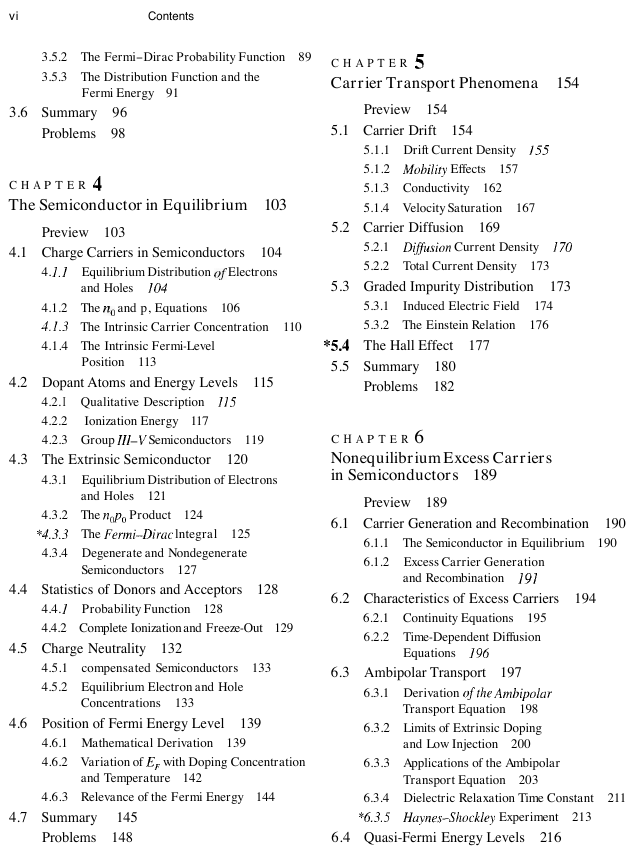
C O N T E N T S
Preface xi
C H A P T E R 1
The Crystal Structure of Solids 1
Preview 1
1.1 Semiconductor Materials 1
1.2 Types of Solids 2
1.3 Space Lattices 3
1.3.1 Primitive and Unit Cell 3
1.3.2 Basic Crystal Structures 4
1.3.3 Crystal Planes and Miller lndices 5
1.3.4 The Diamond Structure 9
1.4 Atomic Bonding 11
"1.5 Imperfections and Impurities in Solids 13
1.5.1
1.5.2
Impegections in Solids 13
lmpurities in Solids 15
*1.6 Growth of Semiconductor Materials 16
1.6.1 Growthfrom a Melt 16
1.6.2 Epitaxial Growth 18
1.7 Summary 19
Problems 21
C H A P T E R 2
Introduction to Quantum Mechanics 24
Preview 24
2.1 Principles of Quantum Mechanics 25
2.1.1 Energy Quanta 25
2.1.2 Wave-Particle Duality 26
2.1.3 The Uncertainty Principle 29
2.2 Schrodinger's Wave Equation 30
2.2.1 The Wave Equation 30
2.2.2 Physical Meaning of the Wave
Function 32
2.2.3 Boundary Conditions 32
2.3 Applications of Schrodinger's Wave
Equation 33
2.3.1 Electron in Free Space 33
2.3.2 The Injnite Potential Well 34
2.3.3 The Step Potential Function 38
2.3.4 The Potential Barrier 42
*2.4 Extensions of the Wave Theory to Atoms 45
2.4.1 The One-Electron Atom 45
2.4.2 The Periodic Table 48
2.5 Summary 50
Problems 51
C H A P T E R 3
Introduction to the Quantum Theory
of Solids 56
Preview 56
3.1 Allowed and Forbidden Energy Bands 57
3.1.1 Formation of Energy Bands 57
*3.1.2 The Kronig-Penney Model 61
3.1.3 The k-Space Diagram 66
3.2 Electrical Conduction in Solids 70
3.2.1 The Energy Band and the Bond Model 70
3.2.2 Drift Current 72
3.2.3 Electron Effective Mass 73
3.2.4 Concept of the Hole 76
3.2.5 Metals, Insulators, and
Semiconductors 78
3.3 Extension to Three Dimensions 80
3.3.1 The k-Space Diagrams of Si and GaAs 81
3.3.2 Additional Effective Mass Concepts 82
3.4 Density of States Function 83
3.4.1 Mathematical Derivation 83
3.4.2 Extension to Semiconductors 86
3.5 Statistical Mechanics 88
3.5.1 Statistical Laws 88
�
vi
Contents
3.5.2 The Fermi-Dirac Probability Function 89
3.5.3 The Distribution Function and the
Fermi Energy 91
C H A P T E R 5
Carrier Transport Phenomena 154
3.6 Summary 96
Problems 98
C H A P T E R 4
The Semiconductor in Equilibrium 103
Preview 103
4.1 Charge Carriers in Semiconductors 104
4. I. 1 Equilibrium Distribution of Electrons
and Holes 104
4.1.2 The no and p, Equations 106
3.1.3 The Intrinsic Carrier Concentration 110
4.1.4 The Intrinsic Fermi-Level
Position 113
4.2 Dopant Atoms and Energy Levels 1 15
4.2. I Qualitative Description
4.2.2
Ionization Energy 11 7
4.2.3 Group 111-V Semiconductors 119
I15
4.3 The Extrinsic Semiconductor 120
4.3.1 Equilibrium Distribution of Electrons
and Holes 121
4.3.2 The nap, Product 124
*4.3.3 The Ferrni-Diruc lntegral 125
4.3.4 Degenerate and Nondegenerate
Semiconductors 127
4.4 Statistics of Donors and Acceptors 128
4.4. I Probability Function 128
4.4.2 Complete Ionization and Freeze-Out 129
4.5 Charge Neutrality 132
4.5.1 compensated Semiconductors 133
4.5.2 Equilibrium Electron and Hole
Concentrations 133
4.6 Position of Fermi Energy Level 139
4.6.1 Mathematical Derivation 139
4.6.2 Variation of E, with Doping Concentration
and Temperature 142
4.6.3 Relevance of the Fermi Energy 144
4.7 Summary
145
Problems 148
Preview 154
5.1 Carrier Drift 154
5.1.1 Drift Current Density 155
5.1.2 Mobiliv Effects 157
5.1.3 Conductivity 162
5.1.4 Velocity Saturation 167
5.2 Carrier Diffusion 169
5.2.1 Dzffusion Current Density
5.2.2 Total Current Density 173
I70
5.3 Graded Impurity Distribution 173
5.3.1
Induced Electric Field 174
5.3.2 The Einstein Relation 176
"5.4 The Hall Effect 177
5.5 Summary 180
Problems 182
C H A P T E R 6
Nonequilibrium Excess Carriers
in Semiconductors 189
Preview 189
6.1 Carrier Generation and Recombination 190
6.1.1 The Semiconductor in Equilibrium 190
6.1.2 Excess Carrier Generation
and Recombination 191
6.2 Characteristics of Excess Carriers 194
6.2.1 Continuity Equations 195
6.2.2 Time-Dependent Diffusion
Equations 196
6.3 Ambipolar Transport 197
6.3.1 Derivation ofthe Ambipolar
Transport Equation 198
6.3.2 Limits of Extrinsic Doping
and Low Injection 200
6.3.3 Applications of the Ambipolar
Transport Equation 203
6.3.4 Dielectric Relaxation Time Constant 211
"6.3.5 Huynes-Shockley Experiment 213
6.4 Quasi-Fermi Energy Levels 21 6
�
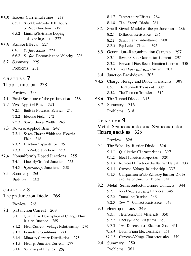
*6.5 Excess-Carrier Lifetime 21 8
6.5.1 Shockley-Read-Hall Theory
of Recombination 21 9
6.5.2 Limits of Extrinsic Doping
and Low Injection 222
"6.6 Surface Effects 224
6.6.1 Su@ceStates
6.6.2 Surjiace Recombination Velocity 226
224
6.7 Summary 229
Problems 231
C H A P T E R 7
The pn Junction 238
Preview 238
7.1 Basic Structure of the pn Junction 238
7.2 Zero Applied Bias 240
7.2.1 Built-in Potential Barrier 240
7.2.2 Electric Field 242
7.2.3 Space Charge Width 246
7.3 Reverse Applied Bias 247
7.3.1 Space Charge Width and Electric
Field 248
7.3.2 Junction Capacitance 251
7.3.3 One-Sided Junctions 253
*7.4 Nonuniformly Doped Junctions 255
7.4.1 Linearly Graded Junction 255
7.4.2 Hyperabrupt Junctions 258
7.5 Summary 260
Problems 262
C H A P T E R 8
The pn Junction Diode 268
Preview 268
8.1 pn Junction Current 269
8.1.1 Qualitative Description of Charge Flow
in a pn Junction 269
Ideal Current-Voltage Relationship 270
8.1.2
8.1.3 Boundary Conditions 271
8.1.4 Minority Carrier Distribution 275
8.1.5
8.1.6 Summary of Physics 281
Ideal pn Junction Current 277
8.1.7 Temperature Effects 284
8.1.8 The "Short" Diode 284
8.2 Small-Signal Model of the pn Junction 286
8.2.1 Diffusion Resistance 286
8.2.2 Small-Signal Admittance 288
8.2.3 Equivalent Circuit 295
8.3 Generation-Recombination Currents 297
8.3.1 Reverse-Bias Generation Current 297
8.3.2 Forward-Bias Recombination Current 300
8.3.3 Total Forwurd-Bias Current 303
8.4 Junction Breakdown 305
"8.5 Charge Storage and Diode Transients 309
8.5.1 The Turn-off Transient 309
8.5.2 The Turn-on Transient 312
"8.6 The Tunnel Diode 3 13
8.7 Summary 3 16
Problems 3 18
C H A P T E R 9
Metal-Semiconductor and Semiconductor
Heterojunctions 326
Preview 326
9.1 The Schottky Barrier Diode 326
Ideal Junction Properties 329
9.1. I Qualitative Characteristics 327
9.1.2
9.1.3 Nonideal Effects on the Barrier Height 333
9.1.4 Current-Voltage Relationship 337
9.1.5 Comparison rdthe Schottky Barrier Diode
and the pn Junction Diode 341
9.2 Metal-Semiconductor Ohmic Contacts 344
Ideal Nonrectifying Barriers 345
9.2.1
9.2.2 Tunneling Barrier 346
9.2.3 Spec$c Contact Resistance 348
9.3 Heterojunctions 349
9.3.1 Heterojunction Materials 350
9.3.2 Energy-Band Diagrams 350
9.3.3 Two-Dimensional Electron Gas 351
*9.3.4 Equilibrium Electrostatics 354
*9.3.5 Current-Voltage Characteristics 359
9.4 Summary 359
Problems 361
�
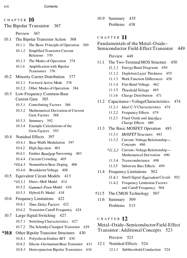
viii
Contents
C H A P T E R 10
The Bipolar Transistor 367
Preview 367
10.1 The Bipolar Transistor Action 368
10.1.1 The Basic Principle of Operation 369
10.1.2 Simplified Transistor Current
Relations 370
10.1.3 The Modes of Operation 374
10.1.4 Amplification with Bipolar
Transistors 376
10.2 Minority Carrier Distribution 377
10.2.1 Forward-Active Mode 378
10.2.2 Other Modes of Operation 384
10.3 Low-Frequency Common-Base
Current Gain 385
10.3.1 Contributing Factors 386
10.3.2 Mathematical Derivation of Current
Gain Factors 388
10.3.3 Summary 392
10.3.4 Example Calculations of the
Gain Factors 393
10.4 Nonideal Effects 397
10.4.1 Base Width Modulation 397
10.4.2 High lnjection 401
10.4.3 Emitter Bandgap Narrowing 403
10.4.4 Current Crowding 405
*10.4.5 Nonuniform Base Doping 406
10.4.6 Breakdown Voltage 408
10.5 Equivalent Circuit Models 41 3
"10.5.1 Ebers-Moll Model 414
10.5.2 Gummel-Poon Model 416
10.5.3 Hybrid-Pi Model 418
10.6 Frequency Limitations 422
10.6.1 Time-DelayFactors 422
10.6.2 Transistor Cutoff Frequency 424
10.7 Large-Signal Switching 427
10.7.1 Switching Characteristics 427
10.7.2 The Schottky-Clamped Transistor 429
*10.8 Other Bipolar Transistor Structures 430
10.9 Summary 435
Problems 438
C H A P T E R 11
Fundamentals of the Metal-Oxide-
Semiconductor Field-Effect Transistor 449
Preview 449
11.1 The Two-Terminal MOS Structure 450
11.1.1 Energy-Band Diagrams 450
11.1.2 Depletion Layer Thickness 455
11.1.3 Work Function Differences 458
11.1.4 Flat-Band Voltage 462
11.1.5 ThresholdVoltage 465
11.1.6 Charge Distribution 471
11.2 Capacitance-Voltage Characteristics 474
Ideal C-V Characteristics 474
11.2.1
11.2.2 Frequency Effects 479
11.2.3 Fixed Oxide and lnte8ace
Charge Effects 480
11.3 The Basic MOSFET Operation 483
11.3.1 MOSFETStructures 483
11.3.2 Current-Voltage Relationship-
Concepts 486
"11.3.3 Current-Voltage Relationship-
Mathematical Derivation 490
11.3.4 Transconductance 498
11.3.5 Substrate Bias Effects 499
11.4 Frequency Limitations 502
11.4.1 Small-Signal Equivalerzt Circuit 502
11.4.2 Frequency Limitation Factors
and Cutoff Frequency 504
'11.5 The CMOS Technology 507
4
11.6 Summary 509
Problems 5 13
C H A P T E R 12
Metal-Oxide-Semiconductor Field-Effect
Transistor: Additional Concepts 523
10.8.1 Polysilicon Emitter BJT 430
10.8.2 Silicon-Germanium Base Transistor 431
10.8.3 Heterojunction Bipolar Transistors 434
Preview 523
12.1 Nonideal Effects 524
12.1.1 Subthreshold Conduction 524
�



 2023年江西萍乡中考道德与法治真题及答案.doc
 2012年重庆南川中考生物真题及答案.doc
 2013年江西师范大学地理学综合及文艺理论基础考研真题.doc
 2020年四川甘孜小升初语文真题及答案I卷.doc
 2020年注册岩土工程师专业基础考试真题及答案.doc
 2023-2024学年福建省厦门市九年级上学期数学月考试题及答案.doc
 2021-2022学年辽宁省沈阳市大东区九年级上学期语文期末试题及答案.doc
 2022-2023学年北京东城区初三第一学期物理期末试卷及答案.doc
 2018上半年江西教师资格初中地理学科知识与教学能力真题及答案.doc
 2012年河北国家公务员申论考试真题及答案-省级.doc
 2020-2021学年江苏省扬州市江都区邵樊片九年级上学期数学第一次质量检测试题及答案.doc
 2022下半年黑龙江教师资格证中学综合素质真题及答案.doc