logo资料库

Hspice model说明.pdf

第1页 / 共734页
第2页 / 共734页
第3页 / 共734页
第4页 / 共734页
第5页 / 共734页
第6页 / 共734页
第7页 / 共734页
第8页 / 共734页
资料共734页,剩余部分请下载后查看
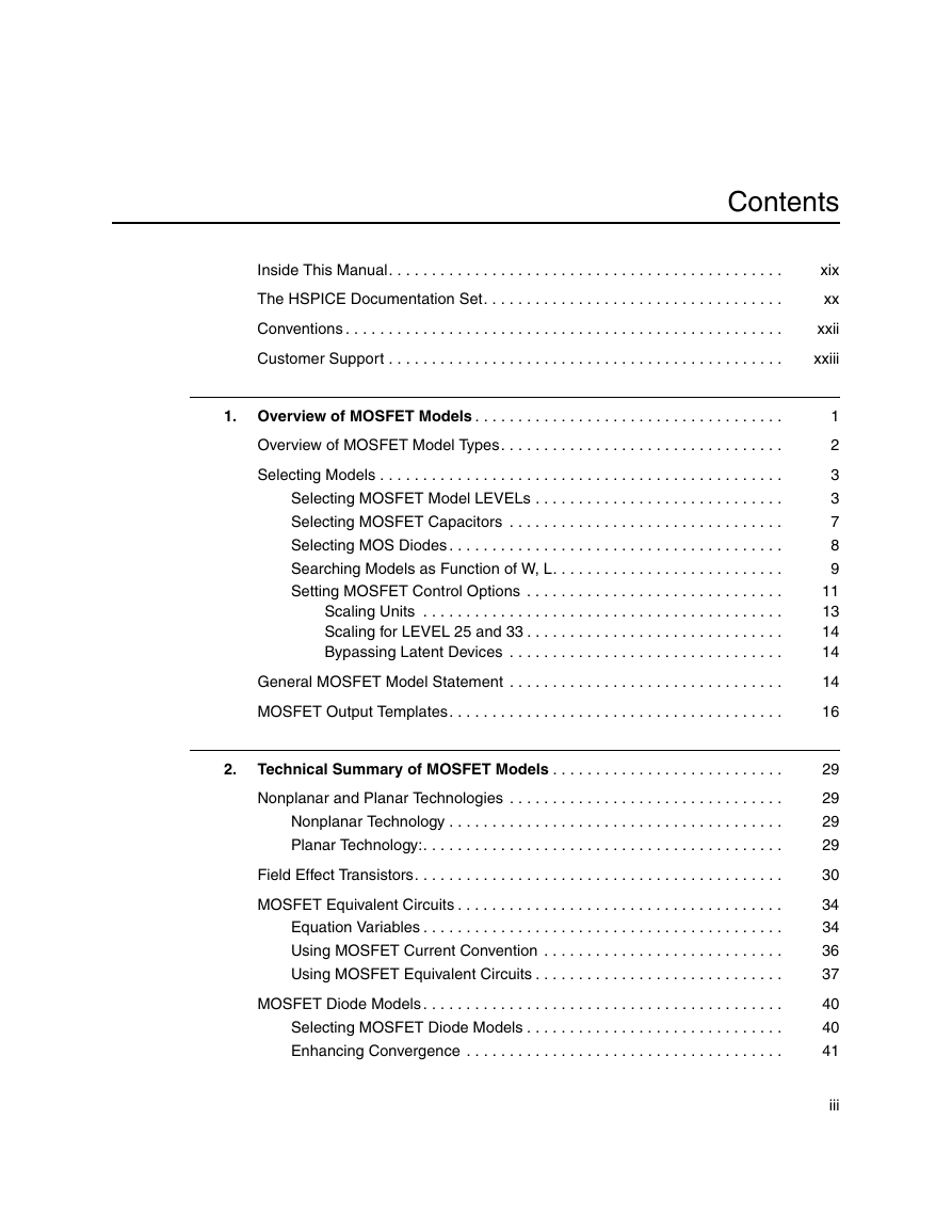
Contents
Inside This Manual
The HSPICE Documentation Set
Conventions
Customer Support
1 Overview of MOSFET Models
Overview of MOSFET Model Types
Selecting Models
Selecting MOSFET Model LEVELs
Selecting MOSFET Capacitors
Selecting MOS Diodes
Searching Models as Function of W, L
Setting MOSFET Control Options
Scaling Units
Scaling for LEVEL 25 and 33
Bypassing Latent Devices
General MOSFET Model Statement
MOSFET Output Templates
2 Technical Summary of MOSFET Models
Nonplanar and Planar Technologies
Nonplanar Technology
Planar Technology:
Field Effect Transistors
MOSFET Equivalent Circuits
Equation Variables
Using MOSFET Current Convention
Using MOSFET Equivalent Circuits
MOSFET Diode Models
Selecting MOSFET Diode Models
Enhancing Convergence
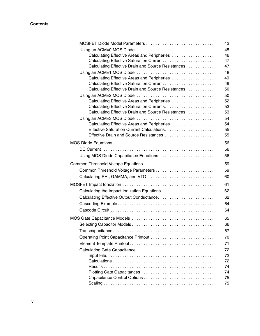
MOSFET Diode Model Parameters
Using an ACM=0 MOS Diode
Calculating Effective Areas and Peripheries
Calculating Effective Saturation Current
Calculating Effective Drain and Source Resistances
Using an ACM=1 MOS Diode
Calculating Effective Areas and Peripheries
Calculating Effective Saturation Current
Calculating Effective Drain and Source Resistances
Using an ACM=2 MOS Diode
Calculating Effective Areas and Peripheries
Calculating Effective Saturation Currents
Calculating Effective Drain and Source Resistances
Using an ACM=3 MOS Diode
Calculating Effective Areas and Peripheries
Effective Saturation Current Calculations
Effective Drain and Source Resistances
MOS Diode Equations
DC Current
Using MOS Diode Capacitance Equations
Common Threshold Voltage Equations
Common Threshold Voltage Parameters
Calculating PHI, GAMMA, and VTO
MOSFET Impact Ionization
Calculating the Impact Ionization Equations
Calculating Effective Output Conductance
Cascoding Example
Cascode Circuit
MOS Gate Capacitance Models
Selecting Capacitor Models
Transcapacitance
Operating Point Capacitance Printout
Element Template Printout
Calculating Gate Capacitance
Input File
Calculations
Results
Plotting Gate Capacitances
Capacitance Control Options
Scaling
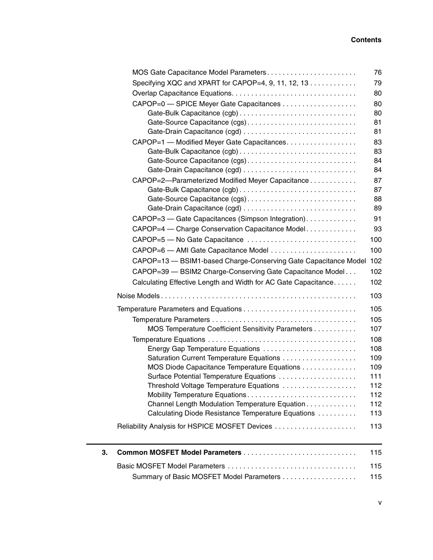
MOS Gate Capacitance Model Parameters
Specifying XQC and XPART for CAPOP=4, 9, 11, 12, 13
Overlap Capacitance Equations
CAPOP=0 - SPICE Meyer Gate Capacitances
Gate-Bulk Capacitance (cgb)
Gate-Source Capacitance (cgs)
Gate-Drain Capacitance (cgd)
CAPOP=1 - Modified Meyer Gate Capacitances
Gate-Bulk Capacitance (cgb)
Gate-Source Capacitance (cgs)
Gate-Drain Capacitance (cgd)
CAPOP=2-Parameterized Modified Meyer Capacitance
Gate-Bulk Capacitance (cgb)
Gate-Source Capacitance (cgs)
Gate-Drain Capacitance (cgd)
CAPOP=3 - Gate Capacitances (Simpson Integration)
CAPOP=4 - Charge Conservation Capacitance Model
CAPOP=5 - No Gate Capacitance
CAPOP=6 - AMI Gate Capacitance Model
CAPOP=13 - BSIM1-based Charge-Conserving Gate Capacitance Model
CAPOP=39 - BSIM2 Charge-Conserving Gate Capacitance Model
Calculating Effective Length and Width for AC Gate Capacitance
Noise Models
Temperature Parameters and Equations
Temperature Parameters
MOS Temperature Coefficient Sensitivity Parameters
Temperature Equations
Energy Gap Temperature Equations
Saturation Current Temperature Equations
MOS Diode Capacitance Temperature Equations
Surface Potential Temperature Equations
Threshold Voltage Temperature Equations
Mobility Temperature Equations
Channel Length Modulation Temperature Equation
Calculating Diode Resistance Temperature Equations
Reliability Analysis for HSPICE MOSFET Devices
3 Common MOSFET Model Parameters
Basic MOSFET Model Parameters
Summary of Basic MOSFET Model Parameters
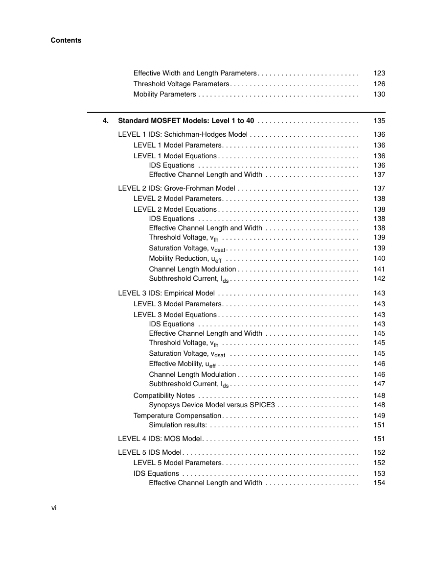
Effective Width and Length Parameters
Threshold Voltage Parameters
Mobility Parameters
4 Standard MOSFET Models: Level 1 to 40
LEVEL 1 IDS: Schichman-Hodges Model
LEVEL 1 Model Parameters
LEVEL 1 Model Equations
IDS Equations
Effective Channel Length and Width
LEVEL 2 IDS: Grove-Frohman Model
LEVEL 2 Model Parameters
LEVEL 2 Model Equations
IDS Equations
Effective Channel Length and Width
Threshold Voltage, vth
Saturation Voltage, vdsat
Mobility Reduction, ueff
Channel Length Modulation
Subthreshold Current, Ids
LEVEL 3 IDS: Empirical Model
LEVEL 3 Model Parameters
LEVEL 3 Model Equations
IDS Equations
Effective Channel Length and Width
Threshold Voltage, vth
Saturation Voltage, vdsat
Effective Mobility, ueff
Channel Length Modulation
Subthreshold Current, Ids
Compatibility Notes
Synopsys Device Model versus SPICE3
Temperature Compensation
Simulation results:
LEVEL 4 IDS: MOS Model
LEVEL 5 IDS Model
LEVEL 5 Model Parameters
IDS Equations
Effective Channel Length and Width
Threshold Voltage, vth
Saturation Voltage, vdsat
Mobility Reduction, UBeff
Channel Length Modulation
Subthreshold Current, Ids
Depletion Mode DC Model ZENH=0
IDS Equations, Depletion Model LEVEL 5
Threshold Voltage, vth
Saturation Voltage, vdsat
Mobility Reduction, UBeff
Channel Length Modulation
Subthreshold Current, Ids
LEVEL 6/LEVEL 7 IDS: MOSFET Model
LEVEL 6 and LEVEL 7 Model Parameters
UPDATE Parameter for LEVEL 6 and LEVEL 7
LEVEL 6 Model Equations, UPDATE=0,2
IDS Equations
Effective Channel Length and Width
Threshold Voltage, vth
Single-Gamma, VBO=0
Effective Built-in Voltage, vbi
Multi-Level Gamma, VBO>0
Effective Built-in Voltage, vbi for VBO>0
Saturation Voltage, vdsat (UPDATE=0,2)
Saturation Voltage, vsat
LEVEL 6 IDS Equations, UPDATE=1
Alternate DC Model (ISPICE model)
Subthreshold Current, ids
Effective Mobility, ueff
Channel Length Modulation
ASPEC Compatibility
LEVEL 7 IDS Model
LEVEL 8 IDS Model
LEVEL 8 Model Parameters
LEVEL 8 Model Equations
IDS Equations
Effective Channel Length and Width
Effective Substrate Doping, nsub
Threshold Voltage, vth
Saturation Voltage vdsat
Effective Mobility, ueff
Channel Length Modulation
Subthreshold Current Ids
LEVEL 27 SOSFET Model
LEVEL 27 Model Parameters
Non-Fully Depleted SOI Model
Model Components
Obtaining Model Parameters
Fully Depleted SOI Model Considerations
LEVEL 38 IDS: Cypress Depletion Model
LEVEL 38 Model Parameters
LEVEL 38 Model Equations
IDS Equations
Threshold Voltage, vth
Saturation Voltage, vdsat
Mobility Reduction, UBeff
Channel Length Modulation
Subthreshold Current, ids
Example Model File
Mobility Model
Body Effect
Saturation
LEVEL 40 HP a-Si TFT Model
Using the HP a-Si TFT Model
Effect of SCALE and SCALM
Noise Model
DELVTO Element
Device Model and Element Statement Example
LEVEL 40 Model Equations
Cutoff Region (NFS=0, vgs £ von)
Noncutoff Region (NFS ¹ 0)
Cgd, Cgs
LEVEL 40 Model Topology
References
5 Standard MOSFET Models: Levels 50 to 69
Level 50 Philips MOS9 Model
JUNCAP Model Parameters
Using the Philips MOS9 Model
Model Statement Example
Level 55 EPFL-EKV MOSFET Model
Single Equation Model
Effects Modeled
Coherence of Static and Dynamic Models
Bulk Reference and Symmetry
EKV Intrinsic Model Parameters
Static Intrinsic Model Equations
Parameter Preprocessing
Bulk Referenced Intrinsic Voltages
Effective Channel Length and Width
Short Distance Matching
Reverse Short-channel Effect (RSCE)
Effective Gate Voltage Including RSCE
Effective substrate factor including charge-sharing for short and narrow channels
Pinch-off Voltage Including Short-Channel and Narrow-Channel Effects
Slope Factor
Large Signal Interpolation Function
Forward Normalized Current
Velocity Saturation Voltage
Drain-to-source Saturation Voltage for Reverse Normalized Current
Channel-length Modulation
Equivalent Channel Length Including Channel-length Modulation and Velocity Saturation
Reverse Normalized Current
Transconductance Factor and Mobility Reduction Due to Vertical Field
Specific Current
Drain-to-source Current
Transconductances
Impact Ionization Current
Quasi-static Model Equations
Dynamic Model for the Intrinsic Node Charges
Intrinsic Capacitances
Intrinsic Noise Model Equations
Thermal Noise
Flicker Noise
Operating Point Information
Numerical values of model internal variables
Transconductance efficiency factor
Early voltage
Overdrive voltage
SPICE-like threshold voltage
Saturation voltage
Saturation / non-saturation flag:
Estimation and Limits of Static Intrinsic Model Parameters
Model Updates Description
Revision I, September 1997
Revision II, July 1998
Corrections from EPFL R11, March, 1999
Corrections from EPFL R12, July 30, 1999
Level 58 University of Florida SOI
Level 58 FD/SOI MOSFET Model Parameters
Level 58 NFD/SOI MOSFET Model Parameters
Notes:
Level 58 Template Output
Level 61 RPI a-Si TFT Model
Model Features
Using Level 61 with Synopsys Simulators
Equivalent Circuit
Model Equations
Drain Current
Temperature Dependence
Capacitance
Level 62 RPI Poli-Si TFT Model
Model Features
Using Level 62 with Synopsys Simulators
Equivalent Circuit
Model Equations
Drain Current
Threshold Voltage
Temperature Dependence
Capacitance
Geometry Effect
Self Heating
Level 63 Philips MOS11 Model
Using the Philips MOS11 Model
Description of Parameters
Level 64 STARC HiSIM Model
Level 69 PSP100 Series Model
General Features
PSP100.1 Model
PSP101.0 Model
PSP102.0 Model
PSP102.1 Model
Usage in HSPICE
Instance Parameter Lists
Model Parameter Lists
Source- and Drain-Bulk Junction Model Parameters
6 BSIM MOSFET Models: Levels 13 to 39
LEVEL 13 BSIM Model
BSIM Model Features
LEVEL 13 Model Parameters
Sensitivity Factors of Model Parameters
.MODEL VERSION Changes to BSIM Models
LEVEL 13 Equations
Effective Channel Length and Width
IDS Equations
Threshold Voltage
Saturation Voltage (vdsat)
ids Subthreshold Current
Resistors and Capacitors Generated with Interconnects
Temperature Effect
Charge-Based Capacitance Model
Regions Charge Expressions
Preventing Negative Output Conductance
Calculations Using LEVEL 13 Equations
Compatibility Notes
Model Parameter Naming
SPICE/Synopsys Model Parameter Differences
Parasitics
Temperature Compensation
UPDATE Parameter
IDS and VGS Curves for PMOS and NMOS
LEVEL 28 Modified BSIM Model
LEVEL 28 Features
LEVEL 28 Model Parameters
Notes:
Sensitivity Factors of Model Parameters
LEVEL 28 Model Equations
Effective Channel Length and Width
Threshold Voltage
Effective Mobility
Saturation Voltage (vdsat)
Transition Points
Strong Inversion Current
Weak Inversion Current
LEVEL 39 BSIM2 Model
LEVEL 39 Model Parameters
Other Device Model Parameters that Affect BSIM2
LEVEL 39 Model Equations
Effective Length and Width
Geometry and Bias of Model Parameters
Compatibility Notes
SPICE3 Flag
Temperature
Parasitics
Selecting Gate Capacitance
Unused Parameters
.MODEL VERSION Changes to BSIM2 Models
Preventing Negative Output Conductance
Charge-based Gate Capacitance Model (CAPOP=39)
Synopsys Device Model Enhancements
Temperature Effects
Alternate Gate Capacitance Model
Impact Ionization
Parasitic Diode for Proper LDD Modeling
Skewing of Model Parameters
HSPICE Optimizer
Modeling Guidelines, Removing Mathematical Anomalies
Modeling Example
Typical BSIM2 Model Listing
Common SPICE Parameters
Synopsys Parameters
References
7 MOSFET Models: Levels 47 to 71
Level 47 BSIM3 Version 2 MOS Model
Using the BSIM3 Version 2 MOS Model
Level 47 Notes
Leff and Weff Equations for BSIM3 Version 2.0
Level 47 Model Equations
Threshold Voltage
Mobility of Carrier
Drain Saturation Voltage
Linear Region
Saturation Region
Drain Current
Subthreshold Region
Transition Region (for subthMod=2 only)
Temperature Compensation
PMOS Model
Level 49 and 53 BSIM3v3 MOS Models
Selecting Model Versions
Recommended BSIM3v3 Version
Version 3.2 Features
Version 3.3 Features
Nonquasi-Static (NQS) Model
HSPICE Junction Diode Model and Area Calculation Method
TSMC Diode Model
BSIM3v3 STI/LOD
Parameter Differences
Noise Model
Performance Improvements
Reduced Parameter Set BSIM3v3 Model (BSIM3-lite)
Parameter Binning
BSIM3v3 WPE Model
BSIM3v3 Ig Model
Charge Models
VFBFLAG
Printback
Mobility Multiplier
Using BSIM3v3
Level 49, 53 Model Parameters
Level 49/53 Notes:
Parameter Range Limits
Level 49, 53 Equations
.MODEL CARDS NMOS Model
PMOS Model
Level 54 BSIM4 Model
Version 4.5 Features
General Syntax for BSIM4 Model
Improvements Over BSIM3v3
TSMC Diode Model
BSIM4 Juncap2 Model
BSIM4 STI/LOD
LMLT and WMLT in BSIM4
HSPICE Junction Diode Model and ACM
Level 54 BSIM4 Template Output List
Version 4.6 Features
Level 57 UC Berkeley BSIM3-SOI Model
General Syntax for BSIM3-SOI Model
Level 57 Model Parameters
Level 57 Notes:
Level 57 Template Output
Level 57 Updates to BSIM3-SOI PD versions 2.2, 2.21, and 2.22
Using BSIM3-SOI PD
UCB BSIMSOI3.1
Ideal Full-Depletion (FD) Modeling
Gate Resistance Modeling
Gate Resistance Equivalent Circuit
Enhanced Binning Capability
Bug Fixes
New Features in BSIMSOIv3.2
BSIMSOI3.2 Noise Model
Model Parameters in BSIMSOIv3.2
Level 59 UC Berkeley BSIM3-SOI FD Model
General Syntax for BSIM3-SOI FD Model
Level 59 Model Parameters
Level 59 Template Output
Level 60 UC Berkeley BSIM3-SOI DD Model
Model Features
General Syntax for BSIM3-SOI DD Model
Level 60 BSIMSOI Model Parameters
Level 65 SSIMSOI Model
Using Level 65 with Synopsys Simulators
General Syntax for SSIMSOI
Level 66 HSPICE HVMOS Model
Level 70 BSIMSOI4.0 Model Parameters
General Syntax for BSIMSOI4.0 Model
BSIMOI4.0 Model Parameters
Level 71 TFT Model
General Syntax for the Level 71 Model
Argument Descriptions
Level 71 Model Parameters
BSIM3 and BSIM4 Supported Instance Parameters
8 Custom Common Model Interface
Overview of Custom CMI
Directory Structure
Running Simulations Using Custom CMI Models
Adding Proprietary MOS Models
MOS Models on Unix Platforms
Creating the Directory Environment
Preparing Model Routine Files
Compiling the Shared Library
Choosing a Compiler
Runtime Shared Library Path
Troubleshooting
MOS Models on PC Platforms
Testing Custom CMI Models
Model Interface Routines
Interface Variables
pModel, pInstance
CMI_ResetModel
CMI_ResetInstance
CMI_AssignModelParm
CMI_AssignInstanceParm
CMI_SetupModel
CMI_SetupInstance
CMI_Evaluate
CMI_DiodeEval
CMI_Noise
CMI_PrintModel
CMI_FreeModel
CMI_FreeInstance
CMI_WriteError
CMI_Start
CMI_Conclude
Custom CMI Function Calling Protocol
Internal Routines
Extended Topology
Enhancements for Custom CMI
Gate Direct Tunneling Current
Additional Instance Parameter Support
An Extension to Support BSIM4 Topology
Activating These Enhancements
Conventions
Bias Polarity, for N- and P-channel Devices
Source-Drain Reversal Conventions
Thread-Safe Model Code
A Finding Device Libraries
The HSPICE Automatic Model Selector
B Comparing MOS Models
History and Motivation
Synopsys Device Model Enhancements
LEVEL 2
LEVEL 3
LEVEL 13 (BSIM)
LEVEL 28
LEVEL 39
Future for Model Developments
Model Equation Evaluation Criteria
Potential for Good Fit to Data
Measure: Number of Parameters
Measure: Minimal Number of Parameters
Ease of Fit to Data
Measure: Physical Percentage of Parameters
Robustness and Convergence Properties
Behavior Follows Devices in All Circuit Conditions
Ability to Simulate Process Variation
Gate Capacitance Modeling
Outline of Optimization Procedure
Examples of Data Fitting
LEVEL 28, 2, 3-Ids Model vs. Data
LEVEL 13, 28, 39 - Ids Model vs. Data
LEVEL 2, 3, 28-Gds Model vs. Data
LEVEL 13, 28, 39-Gds Model versus Data
LEVEL 2, 3, 28- Ids Model versus Data
LEVEL 13, 28, 39-Ids Model versus Data
LEVEL 2, 3, 28-Gm/Ids Model versus Data
LEVEL 13, 28, 39-Gm/Ids Model versus Data
Gds versus Vds at Vgs=4, Vbs=0
Gm/Ids vs. Vgs at Vds=0.1, Vbs=0, 2
Gm/Ids versus Vgs at Vds=0.1, Vbs=0
Index
A
B
C
D
E
F
G
H
I
J
L
M
N
O
P
Q
R
S
T
U
V
W
X
HSPICE® MOSFET Models Manual Version Z-2006.03, March 2007
Copyright Notice and Proprietary Information Copyright © 2007 Synopsys, Inc. All rights reserved. This software and documentation contain confidential and proprietary information that is the property of Synopsys, Inc. The software and documentation are furnished under a license agreement and may be used or copied only in accordance with the terms of the license agreement. No part of the software and documentation may be reproduced, transmitted, or translated, in any form or by any means, electronic, mechanical, manual, optical, or otherwise, without prior written permission of Synopsys, Inc., or as expressly provided by the license agreement. Right to Copy Documentation The license agreement with Synopsys permits licensee to make copies of the documentation for its internal use only. Each copy shall include all copyrights, trademarks, service marks, and proprietary rights notices, if any. Licensee must assign sequential numbers to all copies. These copies shall contain the following legend on the cover page: “This document is duplicated with the permission of Synopsys, Inc., for the exclusive use of __________________________________________ and its employees. This is copy number __________.” Destination Control Statement All technical data contained in this publication is subject to the export control laws of the United States of America. Disclosure to nationals of other countries contrary to United States law is prohibited. It is the reader’s responsibility to determine the applicable regulations and to comply with them. Disclaimer SYNOPSYS, INC., AND ITS LICENSORS MAKE NO WARRANTY OF ANY KIND, EXPRESS OR IMPLIED, WITH REGARD TO THIS MATERIAL, INCLUDING, BUT NOT LIMITED TO, THE IMPLIED WARRANTIES OF MERCHANTABILITY AND FITNESS FOR A PARTICULAR PURPOSE. Registered Trademarks (®) Synopsys, AMPS, Cadabra, CATS, CRITIC, CSim, Design Compiler, DesignPower, DesignWare, EPIC, Formality, HSIM, HSPICE, iN-Phase, in-Sync, Leda, MAST, ModelTools, NanoSim, OpenVera, PathMill, Photolynx, Physical Compiler, PrimeTime, SiVL, SNUG, SolvNet, System Compiler, TetraMAX, VCS, Vera, and YIELDirector are registered trademarks of Synopsys, Inc. Trademarks (™) AFGen, Apollo, Astro, Astro-Rail, Astro-Xtalk, Aurora, AvanWaves, Columbia, Columbia-CE, Cosmos, CosmosEnterprise, CosmosLE, CosmosScope, CosmosSE, DC Expert, DC Professional, DC Ultra, Design Analyzer, Design Vision, DesignerHDL, Direct Silicon Access, Discovery, Encore, Galaxy, HANEX, HDL Compiler, Hercules, Hierarchical Optimization Technology, HSIMplus, HSPICE-Link, iN-Tandem, i-Virtual Stepper, Jupiter, Jupiter-DP, JupiterXT, JupiterXT-ASIC, Liberty, Libra-Passport, Library Compiler, Magellan, Mars, Mars-Xtalk, Milkyway, ModelSource, Module Compiler, Planet, Planet-PL, Polaris, Power Compiler, Raphael, Raphael-NES, Saturn, Scirocco, Scirocco-i, Star-RCXT, Star-SimXT, Taurus, TSUPREM-4, VCS Express, VCSi, VHDL Compiler, VirSim, and VMC are trademarks of Synopsys, Inc. Service Marks (SM) MAP-in, SVP Café, and TAP-in are service marks of Synopsys, Inc. SystemC is a trademark of the Open SystemC Initiative and is used under license. ARM and AMBA are registered trademarks of ARM Limited. Saber is a registered trademark of SabreMark Limited Partnership and is used under license. All other product or company names may be trademarks of their respective owners. Printed in the U.S.A. HSPICE® MOSFET Models Manual, Z-2006.03 ii HSPICE® MOSFET Models Manual Z-2006.03
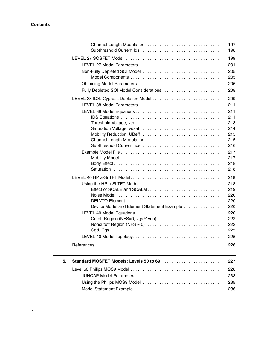
Contents Inside This Manual. . . . . . . . . . . . . . . . . . . . . . . . . . . . . . . . . . . . . . . . . . . . . . The HSPICE Documentation Set. . . . . . . . . . . . . . . . . . . . . . . . . . . . . . . . . . . Conventions . . . . . . . . . . . . . . . . . . . . . . . . . . . . . . . . . . . . . . . . . . . . . . . . . . . Customer Support . . . . . . . . . . . . . . . . . . . . . . . . . . . . . . . . . . . . . . . . . . . . . . xix xx xxii xxiii 1. Overview of MOSFET Models . . . . . . . . . . . . . . . . . . . . . . . . . . . . . . . . . . . . Overview of MOSFET Model Types. . . . . . . . . . . . . . . . . . . . . . . . . . . . . . . . . Selecting Models . . . . . . . . . . . . . . . . . . . . . . . . . . . . . . . . . . . . . . . . . . . . . . . Selecting MOSFET Model LEVELs . . . . . . . . . . . . . . . . . . . . . . . . . . . . . Selecting MOSFET Capacitors . . . . . . . . . . . . . . . . . . . . . . . . . . . . . . . . Selecting MOS Diodes . . . . . . . . . . . . . . . . . . . . . . . . . . . . . . . . . . . . . . . Searching Models as Function of W, L. . . . . . . . . . . . . . . . . . . . . . . . . . . Setting MOSFET Control Options . . . . . . . . . . . . . . . . . . . . . . . . . . . . . . Scaling Units . . . . . . . . . . . . . . . . . . . . . . . . . . . . . . . . . . . . . . . . . . Scaling for LEVEL 25 and 33 . . . . . . . . . . . . . . . . . . . . . . . . . . . . . . Bypassing Latent Devices . . . . . . . . . . . . . . . . . . . . . . . . . . . . . . . . General MOSFET Model Statement . . . . . . . . . . . . . . . . . . . . . . . . . . . . . . . . MOSFET Output Templates. . . . . . . . . . . . . . . . . . . . . . . . . . . . . . . . . . . . . . . 2. Technical Summary of MOSFET Models . . . . . . . . . . . . . . . . . . . . . . . . . . . Nonplanar and Planar Technologies . . . . . . . . . . . . . . . . . . . . . . . . . . . . . . . . Nonplanar Technology . . . . . . . . . . . . . . . . . . . . . . . . . . . . . . . . . . . . . . . Planar Technology:. . . . . . . . . . . . . . . . . . . . . . . . . . . . . . . . . . . . . . . . . . Field Effect Transistors. . . . . . . . . . . . . . . . . . . . . . . . . . . . . . . . . . . . . . . . . . . MOSFET Equivalent Circuits . . . . . . . . . . . . . . . . . . . . . . . . . . . . . . . . . . . . . . Equation Variables . . . . . . . . . . . . . . . . . . . . . . . . . . . . . . . . . . . . . . . . . . Using MOSFET Current Convention . . . . . . . . . . . . . . . . . . . . . . . . . . . . Using MOSFET Equivalent Circuits . . . . . . . . . . . . . . . . . . . . . . . . . . . . . MOSFET Diode Models . . . . . . . . . . . . . . . . . . . . . . . . . . . . . . . . . . . . . . . . . . Selecting MOSFET Diode Models . . . . . . . . . . . . . . . . . . . . . . . . . . . . . . Enhancing Convergence . . . . . . . . . . . . . . . . . . . . . . . . . . . . . . . . . . . . . 1 2 3 3 7 8 9 11 13 14 14 14 16 29 29 29 29 30 34 34 36 37 40 40 41 iii
Contents iv MOSFET Diode Model Parameters . . . . . . . . . . . . . . . . . . . . . . . . . . . . . Using an ACM=0 MOS Diode . . . . . . . . . . . . . . . . . . . . . . . . . . . . . . . . . Calculating Effective Areas and Peripheries . . . . . . . . . . . . . . . . . . Calculating Effective Saturation Current. . . . . . . . . . . . . . . . . . . . . . Calculating Effective Drain and Source Resistances . . . . . . . . . . . . Using an ACM=1 MOS Diode . . . . . . . . . . . . . . . . . . . . . . . . . . . . . . . . . Calculating Effective Areas and Peripheries . . . . . . . . . . . . . . . . . . Calculating Effective Saturation Current. . . . . . . . . . . . . . . . . . . . . . Calculating Effective Drain and Source Resistances . . . . . . . . . . . . Using an ACM=2 MOS Diode . . . . . . . . . . . . . . . . . . . . . . . . . . . . . . . . . Calculating Effective Areas and Peripheries . . . . . . . . . . . . . . . . . . Calculating Effective Saturation Currents. . . . . . . . . . . . . . . . . . . . . Calculating Effective Drain and Source Resistances . . . . . . . . . . . . Using an ACM=3 MOS Diode . . . . . . . . . . . . . . . . . . . . . . . . . . . . . . . . . Calculating Effective Areas and Peripheries . . . . . . . . . . . . . . . . . . Effective Saturation Current Calculations. . . . . . . . . . . . . . . . . . . . . Effective Drain and Source Resistances . . . . . . . . . . . . . . . . . . . . . MOS Diode Equations . . . . . . . . . . . . . . . . . . . . . . . . . . . . . . . . . . . . . . . . . . . DC Current . . . . . . . . . . . . . . . . . . . . . . . . . . . . . . . . . . . . . . . . . . . . . . . . Using MOS Diode Capacitance Equations . . . . . . . . . . . . . . . . . . . . . . . Common Threshold Voltage Equations . . . . . . . . . . . . . . . . . . . . . . . . . . . . . . Common Threshold Voltage Parameters . . . . . . . . . . . . . . . . . . . . . . . . . Calculating PHI, GAMMA, and VTO . . . . . . . . . . . . . . . . . . . . . . . . . . . . MOSFET Impact Ionization . . . . . . . . . . . . . . . . . . . . . . . . . . . . . . . . . . . . . . . Calculating the Impact Ionization Equations . . . . . . . . . . . . . . . . . . . . . . Calculating Effective Output Conductance. . . . . . . . . . . . . . . . . . . . . . . . Cascoding Example . . . . . . . . . . . . . . . . . . . . . . . . . . . . . . . . . . . . . . . . . Cascode Circuit . . . . . . . . . . . . . . . . . . . . . . . . . . . . . . . . . . . . . . . . . . . . MOS Gate Capacitance Models . . . . . . . . . . . . . . . . . . . . . . . . . . . . . . . . . . . Selecting Capacitor Models . . . . . . . . . . . . . . . . . . . . . . . . . . . . . . . . . . . Transcapacitance . . . . . . . . . . . . . . . . . . . . . . . . . . . . . . . . . . . . . . . . . . . Operating Point Capacitance Printout . . . . . . . . . . . . . . . . . . . . . . . . . . . Element Template Printout . . . . . . . . . . . . . . . . . . . . . . . . . . . . . . . . . . . . Calculating Gate Capacitance . . . . . . . . . . . . . . . . . . . . . . . . . . . . . . . . . Input File. . . . . . . . . . . . . . . . . . . . . . . . . . . . . . . . . . . . . . . . . . . . . . Calculations . . . . . . . . . . . . . . . . . . . . . . . . . . . . . . . . . . . . . . . . . . . Results . . . . . . . . . . . . . . . . . . . . . . . . . . . . . . . . . . . . . . . . . . . . . . . Plotting Gate Capacitances . . . . . . . . . . . . . . . . . . . . . . . . . . . . . . . Capacitance Control Options . . . . . . . . . . . . . . . . . . . . . . . . . . . . . . Scaling . . . . . . . . . . . . . . . . . . . . . . . . . . . . . . . . . . . . . . . . . . . . . . . 42 45 46 47 47 48 49 49 50 50 52 53 53 54 54 55 55 56 56 56 59 59 60 61 62 62 64 64 65 66 67 70 71 72 72 72 74 74 75 75
Contents 76 MOS Gate Capacitance Model Parameters . . . . . . . . . . . . . . . . . . . . . . . 79 Specifying XQC and XPART for CAPOP=4, 9, 11, 12, 13 . . . . . . . . . . . . 80 Overlap Capacitance Equations. . . . . . . . . . . . . . . . . . . . . . . . . . . . . . . . 80 CAPOP=0 — SPICE Meyer Gate Capacitances . . . . . . . . . . . . . . . . . . . 80 Gate-Bulk Capacitance (cgb) . . . . . . . . . . . . . . . . . . . . . . . . . . . . . . 81 Gate-Source Capacitance (cgs) . . . . . . . . . . . . . . . . . . . . . . . . . . . . 81 Gate-Drain Capacitance (cgd) . . . . . . . . . . . . . . . . . . . . . . . . . . . . . 83 CAPOP=1 — Modified Meyer Gate Capacitances. . . . . . . . . . . . . . . . . . 83 Gate-Bulk Capacitance (cgb) . . . . . . . . . . . . . . . . . . . . . . . . . . . . . . 84 Gate-Source Capacitance (cgs) . . . . . . . . . . . . . . . . . . . . . . . . . . . . 84 Gate-Drain Capacitance (cgd) . . . . . . . . . . . . . . . . . . . . . . . . . . . . . 87 CAPOP=2—Parameterized Modified Meyer Capacitance . . . . . . . . . . . . 87 Gate-Bulk Capacitance (cgb) . . . . . . . . . . . . . . . . . . . . . . . . . . . . . . 88 Gate-Source Capacitance (cgs) . . . . . . . . . . . . . . . . . . . . . . . . . . . . 89 Gate-Drain Capacitance (cgd) . . . . . . . . . . . . . . . . . . . . . . . . . . . . . 91 CAPOP=3 — Gate Capacitances (Simpson Integration) . . . . . . . . . . . . . 93 CAPOP=4 — Charge Conservation Capacitance Model . . . . . . . . . . . . . 100 CAPOP=5 — No Gate Capacitance . . . . . . . . . . . . . . . . . . . . . . . . . . . . CAPOP=6 — AMI Gate Capacitance Model . . . . . . . . . . . . . . . . . . . . . . 100 CAPOP=13 — BSIM1-based Charge-Conserving Gate Capacitance Model 102 CAPOP=39 — BSIM2 Charge-Conserving Gate Capacitance Model . . . 102 102 Calculating Effective Length and Width for AC Gate Capacitance. . . . . . Noise Models . . . . . . . . . . . . . . . . . . . . . . . . . . . . . . . . . . . . . . . . . . . . . . . . . . Temperature Parameters and Equations . . . . . . . . . . . . . . . . . . . . . . . . . . . . . Temperature Parameters . . . . . . . . . . . . . . . . . . . . . . . . . . . . . . . . . . . . . MOS Temperature Coefficient Sensitivity Parameters . . . . . . . . . . . Temperature Equations . . . . . . . . . . . . . . . . . . . . . . . . . . . . . . . . . . . . . . Energy Gap Temperature Equations . . . . . . . . . . . . . . . . . . . . . . . . Saturation Current Temperature Equations . . . . . . . . . . . . . . . . . . . MOS Diode Capacitance Temperature Equations . . . . . . . . . . . . . . Surface Potential Temperature Equations . . . . . . . . . . . . . . . . . . . . Threshold Voltage Temperature Equations . . . . . . . . . . . . . . . . . . . Mobility Temperature Equations . . . . . . . . . . . . . . . . . . . . . . . . . . . . Channel Length Modulation Temperature Equation . . . . . . . . . . . . . Calculating Diode Resistance Temperature Equations . . . . . . . . . . Reliability Analysis for HSPICE MOSFET Devices . . . . . . . . . . . . . . . . . . . . . 3. Common MOSFET Model Parameters . . . . . . . . . . . . . . . . . . . . . . . . . . . . . Basic MOSFET Model Parameters . . . . . . . . . . . . . . . . . . . . . . . . . . . . . . . . . Summary of Basic MOSFET Model Parameters . . . . . . . . . . . . . . . . . . . 103 105 105 107 108 108 109 109 111 112 112 112 113 113 115 115 115 v
Contents vi Effective Width and Length Parameters . . . . . . . . . . . . . . . . . . . . . . . . . . Threshold Voltage Parameters. . . . . . . . . . . . . . . . . . . . . . . . . . . . . . . . . Mobility Parameters . . . . . . . . . . . . . . . . . . . . . . . . . . . . . . . . . . . . . . . . . 4. Standard MOSFET Models: Level 1 to 40 . . . . . . . . . . . . . . . . . . . . . . . . . . LEVEL 1 IDS: Schichman-Hodges Model . . . . . . . . . . . . . . . . . . . . . . . . . . . . LEVEL 1 Model Parameters. . . . . . . . . . . . . . . . . . . . . . . . . . . . . . . . . . . LEVEL 1 Model Equations . . . . . . . . . . . . . . . . . . . . . . . . . . . . . . . . . . . . IDS Equations . . . . . . . . . . . . . . . . . . . . . . . . . . . . . . . . . . . . . . . . . Effective Channel Length and Width . . . . . . . . . . . . . . . . . . . . . . . . LEVEL 2 IDS: Grove-Frohman Model . . . . . . . . . . . . . . . . . . . . . . . . . . . . . . . LEVEL 2 Model Parameters. . . . . . . . . . . . . . . . . . . . . . . . . . . . . . . . . . . LEVEL 2 Model Equations . . . . . . . . . . . . . . . . . . . . . . . . . . . . . . . . . . . . IDS Equations . . . . . . . . . . . . . . . . . . . . . . . . . . . . . . . . . . . . . . . . . Effective Channel Length and Width . . . . . . . . . . . . . . . . . . . . . . . . Threshold Voltage, vth . . . . . . . . . . . . . . . . . . . . . . . . . . . . . . . . . . . Saturation Voltage, vdsat. . . . . . . . . . . . . . . . . . . . . . . . . . . . . . . . . . Mobility Reduction, ueff . . . . . . . . . . . . . . . . . . . . . . . . . . . . . . . . . . Channel Length Modulation . . . . . . . . . . . . . . . . . . . . . . . . . . . . . . . Subthreshold Current, Ids . . . . . . . . . . . . . . . . . . . . . . . . . . . . . . . . . LEVEL 3 IDS: Empirical Model . . . . . . . . . . . . . . . . . . . . . . . . . . . . . . . . . . . . LEVEL 3 Model Parameters. . . . . . . . . . . . . . . . . . . . . . . . . . . . . . . . . . . LEVEL 3 Model Equations . . . . . . . . . . . . . . . . . . . . . . . . . . . . . . . . . . . . IDS Equations . . . . . . . . . . . . . . . . . . . . . . . . . . . . . . . . . . . . . . . . . Effective Channel Length and Width . . . . . . . . . . . . . . . . . . . . . . . . Threshold Voltage, vth . . . . . . . . . . . . . . . . . . . . . . . . . . . . . . . . . . . Saturation Voltage, vdsat . . . . . . . . . . . . . . . . . . . . . . . . . . . . . . . . . Effective Mobility, ueff . . . . . . . . . . . . . . . . . . . . . . . . . . . . . . . . . . . . Channel Length Modulation . . . . . . . . . . . . . . . . . . . . . . . . . . . . . . . Subthreshold Current, Ids . . . . . . . . . . . . . . . . . . . . . . . . . . . . . . . . . Compatibility Notes . . . . . . . . . . . . . . . . . . . . . . . . . . . . . . . . . . . . . . . . . Synopsys Device Model versus SPICE3 . . . . . . . . . . . . . . . . . . . . . Temperature Compensation. . . . . . . . . . . . . . . . . . . . . . . . . . . . . . . . . . . Simulation results: . . . . . . . . . . . . . . . . . . . . . . . . . . . . . . . . . . . . . . LEVEL 4 IDS: MOS Model. . . . . . . . . . . . . . . . . . . . . . . . . . . . . . . . . . . . . . . . LEVEL 5 IDS Model. . . . . . . . . . . . . . . . . . . . . . . . . . . . . . . . . . . . . . . . . . . . . LEVEL 5 Model Parameters. . . . . . . . . . . . . . . . . . . . . . . . . . . . . . . . . . . IDS Equations . . . . . . . . . . . . . . . . . . . . . . . . . . . . . . . . . . . . . . . . . . . . . Effective Channel Length and Width . . . . . . . . . . . . . . . . . . . . . . . . 123 126 130 135 136 136 136 136 137 137 138 138 138 138 139 139 140 141 142 143 143 143 143 145 145 145 146 146 147 148 148 149 151 151 152 152 153 154
Contents Threshold Voltage, vth . . . . . . . . . . . . . . . . . . . . . . . . . . . . . . . . . . . Saturation Voltage, vdsat. . . . . . . . . . . . . . . . . . . . . . . . . . . . . . . . . . Mobility Reduction, UBeff . . . . . . . . . . . . . . . . . . . . . . . . . . . . . . . . . Channel Length Modulation . . . . . . . . . . . . . . . . . . . . . . . . . . . . . . . Subthreshold Current, Ids . . . . . . . . . . . . . . . . . . . . . . . . . . . . . . . . . Depletion Mode DC Model ZENH=0 . . . . . . . . . . . . . . . . . . . . . . . . . . . . IDS Equations, Depletion Model LEVEL 5 . . . . . . . . . . . . . . . . . . . . . . . . Threshold Voltage, vth . . . . . . . . . . . . . . . . . . . . . . . . . . . . . . . . . . . Saturation Voltage, vdsat . . . . . . . . . . . . . . . . . . . . . . . . . . . . . . . . . Mobility Reduction, UBeff . . . . . . . . . . . . . . . . . . . . . . . . . . . . . . . . . Channel Length Modulation . . . . . . . . . . . . . . . . . . . . . . . . . . . . . . Subthreshold Current, Ids . . . . . . . . . . . . . . . . . . . . . . . . . . . . . . . . . LEVEL 6/LEVEL 7 IDS: MOSFET Model. . . . . . . . . . . . . . . . . . . . . . . . . . . . . LEVEL 6 and LEVEL 7 Model Parameters. . . . . . . . . . . . . . . . . . . . . . . . UPDATE Parameter for LEVEL 6 and LEVEL 7 . . . . . . . . . . . . . . . . . . . . LEVEL 6 Model Equations, UPDATE=0,2 . . . . . . . . . . . . . . . . . . . . . . . . IDS Equations . . . . . . . . . . . . . . . . . . . . . . . . . . . . . . . . . . . . . . . . . Effective Channel Length and Width . . . . . . . . . . . . . . . . . . . . . . . . Threshold Voltage, vth . . . . . . . . . . . . . . . . . . . . . . . . . . . . . . . . . . . Single-Gamma, VBO=0 . . . . . . . . . . . . . . . . . . . . . . . . . . . . . . . . . . Effective Built-in Voltage, vbi . . . . . . . . . . . . . . . . . . . . . . . . . . . . . . Multi-Level Gamma, VBO>0. . . . . . . . . . . . . . . . . . . . . . . . . . . . . . . Effective Built-in Voltage, vbi for VBO>0. . . . . . . . . . . . . . . . . . . . . . Saturation Voltage, vdsat (UPDATE=0,2) . . . . . . . . . . . . . . . . . . . . . Saturation Voltage, vsat . . . . . . . . . . . . . . . . . . . . . . . . . . . . . . . . . . LEVEL 6 IDS Equations, UPDATE=1. . . . . . . . . . . . . . . . . . . . . . . . . . . . Alternate DC Model (ISPICE model) . . . . . . . . . . . . . . . . . . . . . . . . Subthreshold Current, ids. . . . . . . . . . . . . . . . . . . . . . . . . . . . . . . . . Effective Mobility, ueff . . . . . . . . . . . . . . . . . . . . . . . . . . . . . . . . . . . . Channel Length Modulation . . . . . . . . . . . . . . . . . . . . . . . . . . . . . . . ASPEC Compatibility . . . . . . . . . . . . . . . . . . . . . . . . . . . . . . . . . . . . . . . . LEVEL 7 IDS Model. . . . . . . . . . . . . . . . . . . . . . . . . . . . . . . . . . . . . . . . . . . . . LEVEL 8 IDS Model. . . . . . . . . . . . . . . . . . . . . . . . . . . . . . . . . . . . . . . . . . . . . LEVEL 8 Model Parameters. . . . . . . . . . . . . . . . . . . . . . . . . . . . . . . . . . . LEVEL 8 Model Equations . . . . . . . . . . . . . . . . . . . . . . . . . . . . . . . . . . . . IDS Equations . . . . . . . . . . . . . . . . . . . . . . . . . . . . . . . . . . . . . . . . . Effective Channel Length and Width . . . . . . . . . . . . . . . . . . . . . . . . Effective Substrate Doping, nsub . . . . . . . . . . . . . . . . . . . . . . . . . . . Threshold Voltage, vth . . . . . . . . . . . . . . . . . . . . . . . . . . . . . . . . . . . Saturation Voltage vdsat . . . . . . . . . . . . . . . . . . . . . . . . . . . . . . . . . Effective Mobility, ueff . . . . . . . . . . . . . . . . . . . . . . . . . . . . . . . . . . . . 154 155 155 156 156 157 158 159 161 161 161 162 164 164 165 167 167 168 168 168 169 170 171 172 177 177 178 179 181 186 191 193 193 194 194 194 194 194 195 195 196 vii
Contents viii Channel Length Modulation . . . . . . . . . . . . . . . . . . . . . . . . . . . . . . . Subthreshold Current Ids . . . . . . . . . . . . . . . . . . . . . . . . . . . . . . . . . LEVEL 27 SOSFET Model. . . . . . . . . . . . . . . . . . . . . . . . . . . . . . . . . . . . . . . . LEVEL 27 Model Parameters. . . . . . . . . . . . . . . . . . . . . . . . . . . . . . . . . . Non-Fully Depleted SOI Model . . . . . . . . . . . . . . . . . . . . . . . . . . . . . . . . Model Components . . . . . . . . . . . . . . . . . . . . . . . . . . . . . . . . . . . . . Obtaining Model Parameters . . . . . . . . . . . . . . . . . . . . . . . . . . . . . . . . . . Fully Depleted SOI Model Considerations . . . . . . . . . . . . . . . . . . . . . . . . LEVEL 38 IDS: Cypress Depletion Model . . . . . . . . . . . . . . . . . . . . . . . . . . . . LEVEL 38 Model Parameters. . . . . . . . . . . . . . . . . . . . . . . . . . . . . . . . . . LEVEL 38 Model Equations . . . . . . . . . . . . . . . . . . . . . . . . . . . . . . . . . . . IDS Equations . . . . . . . . . . . . . . . . . . . . . . . . . . . . . . . . . . . . . . . . . Threshold Voltage, vth . . . . . . . . . . . . . . . . . . . . . . . . . . . . . . . . . . . Saturation Voltage, vdsat . . . . . . . . . . . . . . . . . . . . . . . . . . . . . . . . . Mobility Reduction, UBeff . . . . . . . . . . . . . . . . . . . . . . . . . . . . . . . . . Channel Length Modulation . . . . . . . . . . . . . . . . . . . . . . . . . . . . . . Subthreshold Current, ids. . . . . . . . . . . . . . . . . . . . . . . . . . . . . . . . . Example Model File . . . . . . . . . . . . . . . . . . . . . . . . . . . . . . . . . . . . . . . . . Mobility Model . . . . . . . . . . . . . . . . . . . . . . . . . . . . . . . . . . . . . . . . . Body Effect . . . . . . . . . . . . . . . . . . . . . . . . . . . . . . . . . . . . . . . . . . . . Saturation . . . . . . . . . . . . . . . . . . . . . . . . . . . . . . . . . . . . . . . . . . . . . LEVEL 40 HP a-Si TFT Model. . . . . . . . . . . . . . . . . . . . . . . . . . . . . . . . . . . . . Using the HP a-Si TFT Model . . . . . . . . . . . . . . . . . . . . . . . . . . . . . . . . . Effect of SCALE and SCALM . . . . . . . . . . . . . . . . . . . . . . . . . . . . . . Noise Model . . . . . . . . . . . . . . . . . . . . . . . . . . . . . . . . . . . . . . . . . . . DELVTO Element . . . . . . . . . . . . . . . . . . . . . . . . . . . . . . . . . . . . . . . Device Model and Element Statement Example . . . . . . . . . . . . . . . LEVEL 40 Model Equations . . . . . . . . . . . . . . . . . . . . . . . . . . . . . . . . . . . Cutoff Region (NFS=0, vgs £ von) . . . . . . . . . . . . . . . . . . . . . . . . . . Noncutoff Region (NFS ≠ 0) . . . . . . . . . . . . . . . . . . . . . . . . . . . . . . . Cgd, Cgs . . . . . . . . . . . . . . . . . . . . . . . . . . . . . . . . . . . . . . . . . . . . . LEVEL 40 Model Topology. . . . . . . . . . . . . . . . . . . . . . . . . . . . . . . . . . . . References. . . . . . . . . . . . . . . . . . . . . . . . . . . . . . . . . . . . . . . . . . . . . . . . . . . . 5. Standard MOSFET Models: Levels 50 to 69 . . . . . . . . . . . . . . . . . . . . . . . . Level 50 Philips MOS9 Model . . . . . . . . . . . . . . . . . . . . . . . . . . . . . . . . . . . . . JUNCAP Model Parameters. . . . . . . . . . . . . . . . . . . . . . . . . . . . . . . . . . . Using the Philips MOS9 Model . . . . . . . . . . . . . . . . . . . . . . . . . . . . . . . . Model Statement Example . . . . . . . . . . . . . . . . . . . . . . . . . . . . . . . . . . . . 197 198 199 201 205 205 206 208 209 211 211 211 213 214 215 215 216 217 217 218 218 218 218 219 220 220 220 220 222 222 225 225 226 227 228 233 235 236
分享到:
收藏