The simulation and the realization of the digital filter
With the information age and the advent of the digital world, digital signal processing has
become one of today's most important disciplines and door technology. Digital signal processing
in communications, voice, images, automatic control, radar, military, aerospace, medical and
household appliances, and many other fields widely applied. In the digital signal processing
applications, the digital filter is important and has been widely applied.
1、 figures Unit on :
Analog and digital filters
In signal processing, the function of a filter is to remove unwanted parts of the signal, such as
random noise, or to extract useful parts of the signal, such as the components lying within a certain
frequency range.
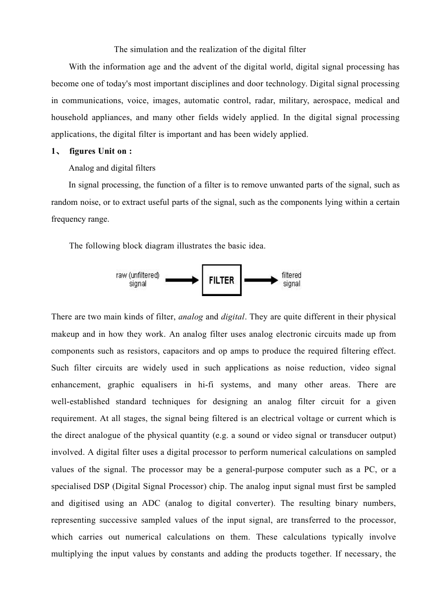
The following block diagram illustrates the basic idea.
in hi-fi
There are two main kinds of filter, analog and digital. They are quite different in their physical
makeup and in how they work. An analog filter uses analog electronic circuits made up from
components such as resistors, capacitors and op amps to produce the required filtering effect.
Such filter circuits are widely used in such applications as noise reduction, video signal
enhancement, graphic equalisers
systems, and many other areas. There are
well-established standard techniques for designing an analog filter circuit
for a given
requirement. At all stages, the signal being filtered is an electrical voltage or current which is
the direct analogue of the physical quantity (e.g. a sound or video signal or transducer output)
involved. A digital filter uses a digital processor to perform numerical calculations on sampled
values of the signal. The processor may be a general-purpose computer such as a PC, or a
specialised DSP (Digital Signal Processor) chip. The analog input signal must first be sampled
and digitised using an ADC (analog to digital converter). The resulting binary numbers,
representing successive sampled values of the input signal, are transferred to the processor,
which carries out numerical calculations on them. These calculations typically involve
multiplying the input values by constants and adding the products together. If necessary, the
�
results of these calculations, which now represent sampled values of the filtered signal, are
output through a DAC (digital to analog converter) to convert the signal back to analog form.
Note that in a digital filter, the signal is represented by a sequence of numbers, rather than
a voltage or current.
The following diagram shows the basic setup of such a system.
Unit refers to the input signals used to filter hardware or software. If the filter input, output
signals are separated, they are bound to respond to the impact of the Unit is separated, such as
digital filters filter definition. Digital filter function, which was to import sequences X
transformation into export operations through a series Y.
According to figures filter function 24-hour live response characteristics, digital filters can
be divided into two, namely, unlimited long live long live the corresponding IIR filter and the
limited response to FIR filters. IIR filters have the advantage of the digital filter design can use
simulation results, and simulation filter design of a large number of tables may facilitate simple.
It is the shortcomings of the nonlinear phase; Linear phase if required, will use the entire
network phase-correction. Image processing and transmission of data collection is required with
linear phase filters identity. And FIR linear phase digital filter to achieve, but an arbitrary
margin characteristics. Impact from the digital filter response of the units can be divided into
two broad categories : the impact of the limited response (FIR) filters, and unlimited number of
shocks to (IIR) digital filters.
FIR filters can be strictly linear phase, but because the system FIR filter function extremity
fixed at the original point, it can only use the higher number of bands to achieve their high
�
selectivity for the same filter design indicators FIR filter called band than a few high-IIR 5-10
times, the cost is higher, Signal delay is also larger. But if the same linear phase, IIR filters must
be network-wide calibration phase, the same section also increase the number of filters and
network complexity. FIR filters can be used to achieve non-Digui way, not in a limited precision
of a shock, and into the homes and quantitative factors of uncertainty arising from the impact of
errors than IIR filter small number, and FIR filter can be used FFT algorithms,
the
computational speed. But unlike IIR filter can filter through the simulation results, there is no
ready-made formula FIR filter must use computer-aided design software (such as MATLAB) to
calculate. So, a broader application of FIR filters, and IIR filters are not very strict requirements
on occasions.
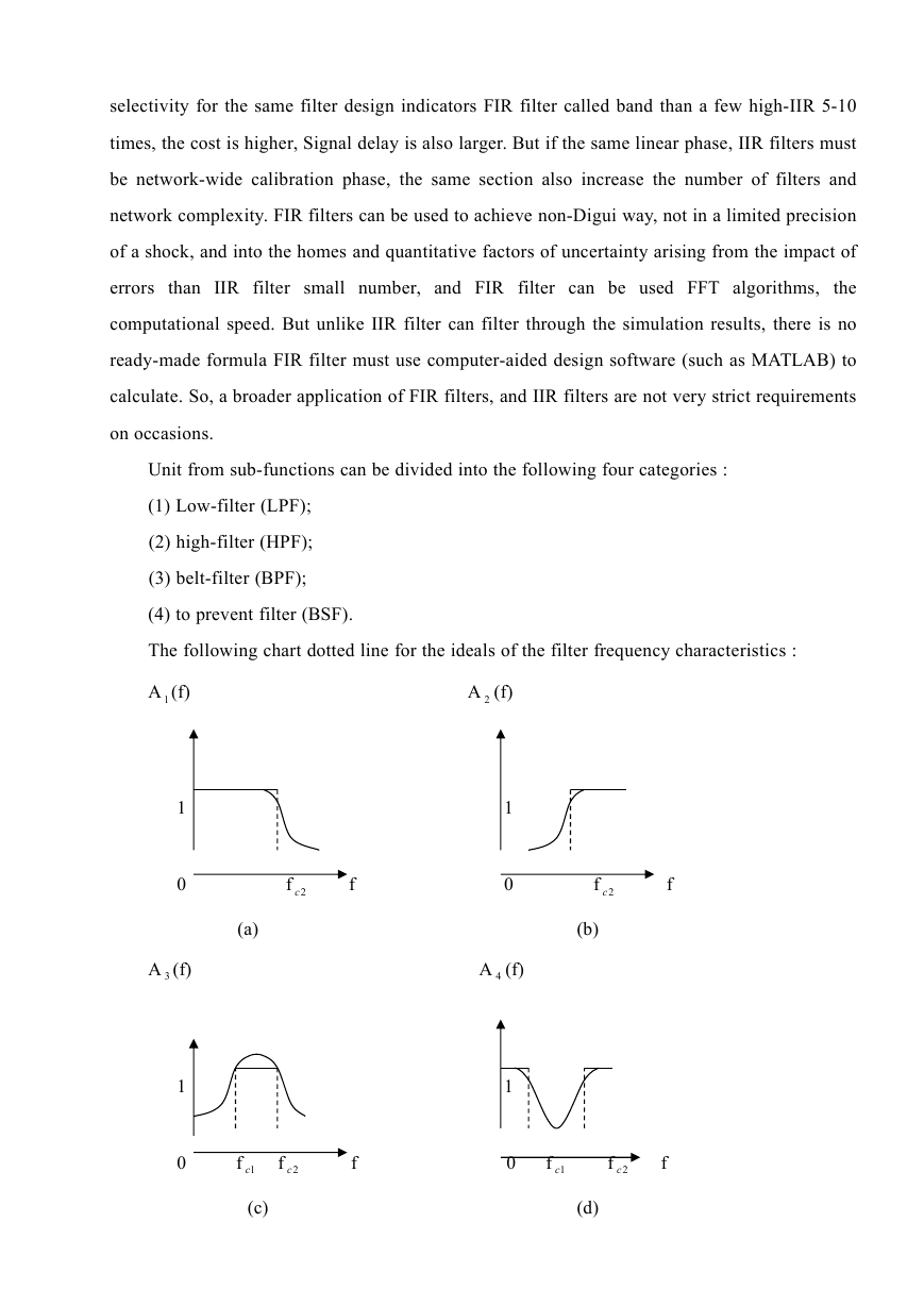
Unit from sub-functions can be divided into the following four categories :
(1) Low-filter (LPF);
(2) high-filter (HPF);
(3) belt-filter (BPF);
(4) to prevent filter (BSF).
The following chart dotted line for the ideals of the filter frequency characteristics :
A 1(f)
1
0
A 3 (f)
1
0
f 2c
f
(a)
f 1c
f 2c
f
(c)
A 2 (f)
1
0
A 4 (f)
1
0
f 2c
f
(b)
f 1c
f 2c
f
(d)
�
(a)LPF (b)HPF (c)BPF (d)BSF
2、 MATLAB introduced
functions,
top mathematical
MATLAB is a matrix laboratory (Matrix Laboratory) is intended. In addition to an
it also provides professional symbols terms, word
excellent value calculation capability,
processing, visualization modeling, simulation and real-time control functions. MATLAB as the
world's
software applications, with a strong engineering computing,
algorithms research, engineering drawings, applications development, data analysis and
dynamic simulation, and other
in aerospace, mechanical manufacturing and
construction fields playing an increasingly important role. And the C language function rich, the
use of flexibility, high-efficiency goals procedures. High language both advantages as well as
low level language features. Therefore, C language is the most widely used programming
language. Although MATLAB is a complete, fully functional programming environment, but in
some cases, data and procedures with the external environment of the world is very necessary
and useful. Filter design using Matlab, could be adjusted with the design requirements and filter
characteristics of the parameters, visual simple, greatly reducing the workload for the filter
design optimization.
In the electricity system protection and secondary computer control, many signal
processing and analysis are based on are certain types Yeroskipou and the second harmonics of
the system voltage and current signals (especially at D process), are mixed with a variety of
complex components, the filter has been installed power system during the critical components.
Current computer protection and the introduction of two digital signal processing software main
filter. Digital filter design using traditional cumbersome formula,
the need to change the
parameters after recalculation, especially in high filters, filter design workload. Uses MATLAB
signal processing boxes can achieve rapid and effective digital filter design and simulation.
MATLAB is the basic unit of data matrix, with its directives Biaodashi mathematics,
engineering, commonly used form is very similar,
is used to solve a problem than in
MATLAB C, Fortran and other languages End precision much the same thing. The popular
MATLAB 5.3/Simulink3.0 including hundreds of internal function with the main pack and 30
types of tool kits (Toolbox). kits can be divided into functional tool kits and disciplines toolkit.
MATLAB tool kit used to expand the functional symbols terms, visualization simulation
it
�
modelling, word processing and real-time control functions. professional disciplines toolkit is a
stronger tool kits, tool kits control, signal processing tool kit, tool kits, etc. belonging to such
communications
MATLAB users to open widely welcomed. In addition to the internal function, all the
packages MATLAB tool kits are readable document and the document could be amended,
modified or users through Yuanchengxu the construction of new procedures to prepare
themselves for kits.
3、 Digital filter design
Digital filter design of the basic requirements
Digital filter design must go through three steps :
(1) Identification of indicators : In the design of a filter, there must be some indicators. These
indicators should be determined on the basis of the application. In many practical applications,
digital filters are often used to achieve the frequency operation. Therefore, indicators in the
form of general jurisdiction given frequency range and phase response. Margins key indicators
given in two ways. The first is absolute indicators. It provides a function to respond to the
demands of the general application of FIR filter design. The second indicator is the relative
indicators. Its value in the form of answers to decibels. In engineering practice, the most popular
of such indicators. For phase response indicators forms, usually in the hope that the system with
a linear phase frequency bands human. Using linear phase filter design with the following
response to the indicators strengths:①it only contains a few algorithms, no plural operations;
②there is delay distortion, only a fixed amount of delay; ③the filter length N (number of bands
for N-1), the volume calculation for N/2 magnitude.
(2) Model approach : Once identified indicators can use a previous study of the basic principles
and relationships, a filter model to be closer to the target system.
(3) Achieved : the results of the above two filters, usually by differential equations, system
function or pulse response to describe. According to this description of hardware or software
used to achieve it.
4、 Introduced FPGA
Programmable logic device is a generic logic can use a variety of chips, which is to achieve
ASIC ASIC (Application Specific Integrated Circuit) semi-customized device, Its emergence
�
and development of electronic systems designers use CAD tools to design their own laboratory
in the ASIC device. Especially FPGA (Field Programmable Gate Array) generated and
development, as a microprocessor, memory, the figures for electronic system design and set a
new industry standard (that is based on standard product sales catalogue in the market to buy).
Is a digital system for microprocessors, memories, FPGA or three standard building blocks
constitute their integration direction.
Digital circuit design using FPGA devices, can not only simplify the design process and
can reduce the size and cost of the entire system, increasing system reliability. They do not need
to spend the traditional sense a lot of time and effort required to create integrated circuits, to
avoid the investment risk and become the fastest-growing industries of electronic devices group.
Digital circuit design system FPGA devices using the following main advantages
(1) Design flexible
Use FPGA devices may not in the standard series device logic functional limitations. And
changes in system design and the use of logic in any one stage of the process, and only through
the use of re-programming the FPGA device can be completed, the system design provides for
great flexibility.
(2)
Increased functional density
Functional density in a given space refers to the number of functional integration logic.
Programmable logic chip components doors several high, a FPGA can replace several films,
film scores or even hundreds of small-scale digital IC chip illustrated in the film. FPGA devices
using the chip to use digital systems in small numbers, thus reducing the number of chips used
to reduce the number of printed size and printed, and will ultimately lead to a reduction in the
overall size of the system.
(3)
Improve reliability
Printing plates and reduce the number of chips, not only can reduce system size, but it
greatly enhanced system reliability. A higher degree of integration than systems in many
low-standard integration components for the design of the same system, with much higher
reliability. FPGA device used to reduce the number of chips required to achieve the system in
the number printed on the cord and joints are reduced, the reliability of the system can be
improved.
(4) Shortening the design cycle
�
As FPGA devices and the programmable flexibility, use it to design a system for longer
than traditional methods greatly shortened. FPGA device master degrees high, use printed
circuit layout wiring simple. At the same time, success in the prototype design, the development
of advanced tools, a high degree of automation, their logic is very simple changes quickly.
Therefore, the use of FPGA devices can significantly shorten the design cycle system, and speed
up the pace of product into the market, improving product competitiveness.
(5) Work fast
FPGA/CPLD devices work fast, generally can reach several original Hertz, far larger than
the DSP device. At the same time, the use of FPGA devices, the system needed to achieve
circuit
classes and small, and thus the pace of work of the entire system will be improved.
(6)
Increased system performance confidentiality
Many FPGA devices have encryption functions in the system widely used FPGA devices
can effectively prevent illegal copying products were others
(7) To reduce costs
FPGA device used to achieve digital system design, if only device itself into the price,
sometimes you would not know it advantages, but there are many factors affecting the cost of
the system, taken together, the cost advantages of using FPGA is obvious. First, the use of
FPGA devices designed to facilitate change, shorten design cycles, reduce development costs
for system development; Secondly, the size and FPGA devices allow automation needs plug-ins,
reducing the manufacturing system to lower costs; Again, the use of FPGA devices can enhance
system reliability, reduced maintenance workload, thereby lowering the cost of maintenance
services for the system. In short, the use of FPGA devices for system design to save costs.
FPGA design principles :
FPGA design an important guiding principles : the balance and size and speed of exchange,
the principles behind the design of the filter expression of a large number of certification.
Here, "area" means a design exertion FPGA/CPLD logic resources of the FPGA can be
used to the typical consumption (FF) and the search table (IUT) to measure more general
measure can be used to design logic equivalence occupied by the door is measured. "pace"
means stability operations in the chip design can achieve the highest frequency, the frequency of
the time series design situation, and design to meet the clock cycle -- PADto pad, Clock Setup
�
Time, Clock Hold Beijing, Clock-to-Output Delay, and other characteristics of many time series
closely related. Area (area) and speed (speed) runs through the two targets FPGA design always
is the ultimate design quality evaluation criteria. On the size and speed of the two basic
concepts : balance of size and speed and size and speed of swap.
One pair of size and speed is the unity of opposites contradictions body. Requirements for
the design of a design while the smallest, highest frequency of operation is unrealistic. More
scientific goal should be to meet the design requirements of the design time series (includes
requirements for the design frequency) premise, the smallest chip area occupied. Or in the
specified area, the design time series cushion greater frequency run higher. This fully embodies
the goals of both size and speed balanced thinking. On the size and speed requirements should
not be simply interpreted as raising the level and design engineers perfect sexual pursuit, and
should recognize that they are products and the quality and cost of direct relevance. If time
series cushion larger design, running relatively high frequency, that the design Jianzhuangxing
stronger, more quality assurance system as a whole; On the other hand, the smaller size of
consumption design is meant to achieve in chip unit more functional modules, the chip needs
fewer, the entire system has been significantly reduced cost. As a contradiction of the two
components, the size and speed is not the same status. In contrast, meet the timetables and work
is more important for some frequency when both conflicts, the use of priority guidelines.
Area and the exchange rate is an important FPGA design ideas. Theoretically, if a design
time series cushion larger, can run much higher than the frequency design requirements, then we
can through the use of functional modules to reduce the consumption of the entire chip design
area, which is used for space savings advantages of speed; Conversely, if the design of a time
series demanding, less than ordinary methods of design frequency then generally flow through
the string and data conversion, parallel reproduction of operational module, designed to take on
the whole "string and conversion" and operate in the export module to chip in the data "and
string conversion" from the macro point of view the whole chip meets the requirements of
processing speed, which is equivalent to the area of reproduction - rate increase.
For example. Assuming that the digital signal processing system is 350Mb/s input data
flow rate, and in FPGA design, data processing modules for maximum processing speed of
150Mb/s, because the data throughput processing module failed to meet requirements, it is
impossible
they should use
to achieve directly in the FPGA. Such circumstances,
�



 2023年江西萍乡中考道德与法治真题及答案.doc
 2012年重庆南川中考生物真题及答案.doc
 2013年江西师范大学地理学综合及文艺理论基础考研真题.doc
 2020年四川甘孜小升初语文真题及答案I卷.doc
 2020年注册岩土工程师专业基础考试真题及答案.doc
 2023-2024学年福建省厦门市九年级上学期数学月考试题及答案.doc
 2021-2022学年辽宁省沈阳市大东区九年级上学期语文期末试题及答案.doc
 2022-2023学年北京东城区初三第一学期物理期末试卷及答案.doc
 2018上半年江西教师资格初中地理学科知识与教学能力真题及答案.doc
 2012年河北国家公务员申论考试真题及答案-省级.doc
 2020-2021学年江苏省扬州市江都区邵樊片九年级上学期数学第一次质量检测试题及答案.doc
 2022下半年黑龙江教师资格证中学综合素质真题及答案.doc