1 Documentation conventions
1.1 List of abbreviations for registers
1.2 Glossary
1.3 Peripheral availability
2 Memory and bus architecture
2.1 System architecture
Figure 1. System architecture
Figure 2. System architecture in connectivity line devices
2.2 Memory organization
2.3 Memory map
Table 1. Register boundary addresses
2.3.1 Embedded SRAM
2.3.2 Bit banding
2.3.3 Embedded Flash memory
Table 2. Flash module organization (low-density devices)
Table 3. Flash module organization (medium-density devices)
Table 4. Flash module organization (high-density devices)
Table 5. Flash module organization (connectivity line devices)
2.4 Boot configuration
Table 6. Boot modes
3 CRC calculation unit
3.1 CRC introduction
3.2 CRC main features
Figure 3. CRC calculation unit block diagram
3.3 CRC functional description
3.4 CRC registers
3.4.1 Data register (CRC_DR)
3.4.2 Independent data register (CRC_IDR)
3.4.3 Control register (CRC_CR)
3.4.4 CRC register map
Table 7. CRC calculation unit register map and reset values
4 Power control (PWR)
4.1 Power supplies
Figure 4. Power supply overview
4.1.1 Independent A/D converter supply and reference voltage
4.1.2 Battery backup domain
4.1.3 Voltage regulator
4.2 Power supply supervisor
4.2.1 Power on reset (POR)/power down reset (PDR)
Figure 5. Power on reset/power down reset waveform
4.2.2 Programmable voltage detector (PVD)
Figure 6. PVD thresholds
4.3 Low-power modes
Table 8. Low-power mode summary
4.3.1 Slowing down system clocks
4.3.2 Peripheral clock gating
4.3.3 Sleep mode
Table 9. Sleep-now
Table 10. Sleep-on-exit
4.3.4 Stop mode
Table 11. Stop mode
4.3.5 Standby mode
Table 12. Standby mode
4.3.6 Auto-wakeup (AWU) from low-power mode
4.4 Power control registers
4.4.1 Power control register (PWR_CR)
4.4.2 Power control/status register (PWR_CSR)
4.4.3 PWR register map
Table 13. PWR register map and reset values
5 Backup registers (BKP)
5.1 BKP introduction
5.2 BKP main features
5.3 BKP functional description
5.3.1 Tamper detection
5.3.2 RTC calibration
5.4 BKP registers
5.4.1 Backup data register x (BKP_DRx) (x = 1 ..42)
Note: The BKP_DRx registers are not reset by a System reset or Power reset or when the device wakes up from Standby mode. They are reset by a Backup Domain reset or by a TAMPER pin event (if the TAMPER pin function is activated).
5.4.2 RTC clock calibration register (BKP_RTCCR)
Note: This bit is reset only by a Backup domain reset.
Note: This bit is reset only by a Backup domain reset.
Note: This bit is reset when the VDD supply is powered off.
5.4.3 Backup control register (BKP_CR)
5.4.4 Backup control/status register (BKP_CSR)
Note: This bit is reset only by a system reset and wakeup from Standby mode.
Note: A Tamper event resets all the BKP_DRx registers. They are held in reset as long as the TEF bit is set. If a write to the BKP_DRx registers is performed while this bit is set, the value will not be stored.
Note: 1: A Tamper interrupt does not wake up the core from low-power modes.
2: This bit is reset only by a system reset and wakeup from Standby mode.
5.4.5 BKP register map
Table 14. BKP register map and reset values
6 Low-, medium- and high-density reset and clock control (RCC)
6.1 Reset
6.1.1 System reset
6.1.2 Power reset
Figure 7. Simplified diagram of the reset circuit
6.1.3 Backup domain reset
6.2 Clocks
Figure 8. Clock tree
6.2.1 HSE clock
Figure 9. HSE/ LSE clock sources
6.2.2 HSI clock
6.2.3 PLL
6.2.4 LSE clock
6.2.5 LSI clock
6.2.6 System clock (SYSCLK) selection
6.2.7 Clock security system (CSS)
6.2.8 RTC clock
6.2.9 Watchdog clock
6.2.10 Clock-out capability
6.3 RCC registers
6.3.1 Clock control register (RCC_CR)
6.3.2 Clock configuration register (RCC_CFGR)
6.3.3 Clock interrupt register (RCC_CIR)
6.3.4 APB2 peripheral reset register (RCC_APB2RSTR)
6.3.5 APB1 peripheral reset register (RCC_APB1RSTR)
6.3.6 AHB peripheral clock enable register (RCC_AHBENR)
6.3.7 APB2 peripheral clock enable register (RCC_APB2ENR)
6.3.8 APB1 peripheral clock enable register (RCC_APB1ENR)
6.3.9 Backup domain control register (RCC_BDCR)
6.3.10 Control/status register (RCC_CSR)
6.3.11 RCC register map
Table 15. RCC register map and reset values
7 Connectivity line devices: reset and clock control (RCC)
7.1 Reset
7.1.1 System reset
7.1.2 Power reset
Figure 10. Simplified diagram of the reset circuit
7.1.3 Backup domain reset
7.2 Clocks
Figure 11. Clock tree
7.2.1 HSE clock
Figure 12. HSE/ LSE clock sources
7.2.2 HSI clock
7.2.3 PLLs
7.2.4 LSE clock
7.2.5 LSI clock
7.2.6 System clock (SYSCLK) selection
7.2.7 Clock security system (CSS)
7.2.8 RTC clock
7.2.9 Watchdog clock
7.2.10 Clock-out capability
7.3 RCC registers
7.3.1 Clock control register (RCC_CR)
7.3.2 Clock configuration register (RCC_CFGR)
7.3.3 Clock interrupt register (RCC_CIR)
7.3.4 APB2 peripheral reset register (RCC_APB2RSTR)
7.3.5 APB1 peripheral reset register (RCC_APB1RSTR)
7.3.6 AHB Peripheral Clock enable register (RCC_AHBENR)
7.3.7 APB2 peripheral clock enable register (RCC_APB2ENR)
7.3.8 APB1 peripheral clock enable register (RCC_APB1ENR)
7.3.9 Backup domain control register (RCC_BDCR)
7.3.10 Control/status register (RCC_CSR)
7.3.11 AHB peripheral clock reset register (RCC_AHBRSTR)
7.3.12 Clock configuration register2 (RCC_CFGR2)
7.3.13 RCC register map
Table 16. RCC register map and reset values
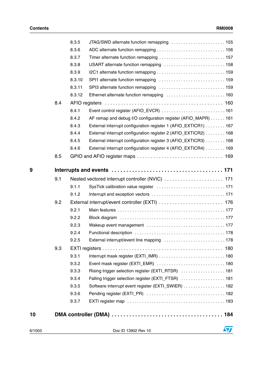
8 General-purpose and alternate-function I/Os (GPIOs and AFIOs)
8.1 GPIO functional description
Figure 13. Basic structure of a standard I/O port bit
Figure 14. Basic structure of a five-volt tolerant I/O port bit
Table 17. Port bit configuration table
Table 18. Output MODE bits
8.1.1 General-purpose I/O (GPIO)
8.1.2 Atomic bit set or reset
8.1.3 External interrupt/wakeup lines
8.1.4 Alternate functions (AF)
8.1.5 Software remapping of I/O alternate functions
8.1.6 GPIO locking mechanism
8.1.7 Input configuration
Figure 15. Input floating/pull up/pull down configurations
8.1.8 Output configuration
Figure 16. Output configuration
8.1.9 Alternate function configuration
Figure 17. Alternate function configuration
8.1.10 Analog configuration
Figure 18. High impedance-analog configuration
8.1.11 Peripherals’ GPIO configurations
Table 19. Advanced timers TIM1/TIM8
Table 20. General-purpose timers TIM2/3/4/5
Table 21. USARTs
Table 22. SPI
Table 23. I2S
Table 24. I2C
Table 25. BxCAN
Table 26. USB
Table 27. OTG_FS pin configuration
Table 28. SDIO
Figure 19. ADC / DAC
Table 29. FSMC
Table 30. Other IOs
8.2 GPIO registers
8.2.1 Port configuration register low (GPIOx_CRL) (x=A..G)
8.2.2 Port configuration register high (GPIOx_CRH) (x=A..G)
8.2.3 Port input data register (GPIOx_IDR) (x=A..G)
8.2.4 Port output data register (GPIOx_ODR) (x=A..G)
8.2.5 Port bit set/reset register (GPIOx_BSRR) (x=A..G)
8.2.6 Port bit reset register (GPIOx_BRR) (x=A..G)
8.2.7 Port configuration lock register (GPIOx_LCKR) (x=A..G)
8.3 Alternate function I/O and debug configuration (AFIO)
8.3.1 Using OSC32_IN/OSC32_OUT pins as GPIO ports PC14/PC15
8.3.2 Using OSC_IN/OSC_OUT pins as GPIO ports PD0/PD1
8.3.3 CAN1 alternate function remapping
Table 31. CAN1 alternate function remapping
8.3.4 CAN2 alternate function remapping
Table 32. CAN2 alternate function remapping
8.3.5 JTAG/SWD alternate function remapping
Table 33. Debug interface signals
Table 34. Debug port mapping
8.3.6 ADC alternate function remapping
Table 35. ADC1 external trigger injected conversion alternate function remapping
Table 36. ADC1 external trigger regular conversion alternate function remapping
Table 37. ADC2 external trigger injected conversion alternate function remapping
Table 38. ADC2 external trigger regular conversion alternate function remapping
8.3.7 Timer alternate function remapping
Table 39. TIM5 alternate function remapping
Table 40. TIM4 alternate function remapping
Table 41. TIM3 alternate function remapping
Table 42. TIM2 alternate function remapping
Table 43. TIM1 alternate function remapping
8.3.8 USART alternate function remapping
Table 44. USART3 remapping
Table 45. USART2 remapping
Table 46. USART1 remapping
8.3.9 I2C1 alternate function remapping
Table 47. I2C1 remapping
8.3.10 SPI1 alternate function remapping
Table 48. SPI1 remapping
8.3.11 SPI3 alternate function remapping
Table 49. SPI3 remapping
8.3.12 Ethernet alternate function remapping
Table 50. ETH remapping
8.4 AFIO registers
8.4.1 Event control register (AFIO_EVCR)
8.4.2 AF remap and debug I/O configuration register (AFIO_MAPR)
8.4.3 External interrupt configuration register 1 (AFIO_EXTICR1)
8.4.4 External interrupt configuration register 2 (AFIO_EXTICR2)
8.4.5 External interrupt configuration register 3 (AFIO_EXTICR3)
8.4.6 External interrupt configuration register 4 (AFIO_EXTICR4)
8.5 GPIO and AFIO register maps
Table 51. GPIO register map and reset values
Table 52. AFIO register map and reset values
9 Interrupts and events
9.1 Nested vectored interrupt controller (NVIC)
9.1.1 SysTick calibration value register
9.1.2 Interrupt and exception vectors
Table 53. Vector table for connectivity line devices
Table 54. Vector table for other STM32F10xxx devices
9.2 External interrupt/event controller (EXTI)
9.2.1 Main features
9.2.2 Block diagram
Figure 20. External interrupt/event controller block diagram
9.2.3 Wakeup event management
9.2.4 Functional description
9.2.5 External interrupt/event line mapping
Figure 21. External interrupt/event GPIO mapping
9.3 EXTI registers
9.3.1 Interrupt mask register (EXTI_IMR)
9.3.2 Event mask register (EXTI_EMR)
9.3.3 Rising trigger selection register (EXTI_RTSR)
9.3.4 Falling trigger selection register (EXTI_FTSR)
9.3.5 Software interrupt event register (EXTI_SWIER)
9.3.6 Pending register (EXTI_PR)
9.3.7 EXTI register map
Table 55. External interrupt/event controller register map and reset values
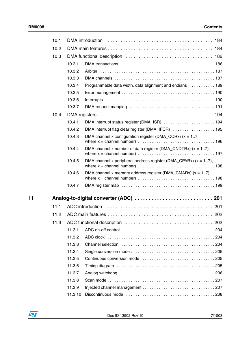
10 DMA controller (DMA)
10.1 DMA introduction
10.2 DMA main features
Figure 22. DMA block diagram in connectivity line devices
Figure 23. DMA block diagram in low-, medium- and high-density devices
10.3 DMA functional description
10.3.1 DMA transactions
10.3.2 Arbiter
10.3.3 DMA channels
10.3.4 Programmable data width, data alignment and endians
Table 56. Programmable data width & endian behavior (when bits PINC = MINC = 1)
10.3.5 Error management
10.3.6 Interrupts
Table 57. DMA interrupt requests
10.3.7 DMA request mapping
Figure 24. DMA1 request mapping
Table 58. Summary of DMA1 requests for each channel
Figure 25. DMA2 request mapping
Table 59. Summary of DMA2 requests for each channel
10.4 DMA registers
10.4.1 DMA interrupt status register (DMA_ISR)
10.4.2 DMA interrupt flag clear register (DMA_IFCR)
10.4.3 DMA channel x configuration register (DMA_CCRx) (x = 1..7, where x = channel number)
10.4.4 DMA channel x number of data register (DMA_CNDTRx) (x = 1..7), where x = channel number)
10.4.5 DMA channel x peripheral address register (DMA_CPARx) (x = 1..7), where x = channel number)
10.4.6 DMA channel x memory address register (DMA_CMARx) (x = 1..7), where x = channel number)
10.4.7 DMA register map
Table 60. DMA register map and reset values
11 Analog-to-digital converter (ADC)
11.1 ADC introduction
11.2 ADC main features
11.3 ADC functional description
Figure 26. Single ADC block diagram
Table 61. ADC pins
11.3.1 ADC on-off control
11.3.2 ADC clock
11.3.3 Channel selection
11.3.4 Single conversion mode
11.3.5 Continuous conversion mode
11.3.6 Timing diagram
Figure 27. Timing diagram
11.3.7 Analog watchdog
Figure 28. Analog watchdog guarded area
Table 62. Analog watchdog channel selection
11.3.8 Scan mode
11.3.9 Injected channel management
Figure 29. Injected conversion latency
11.3.10 Discontinuous mode
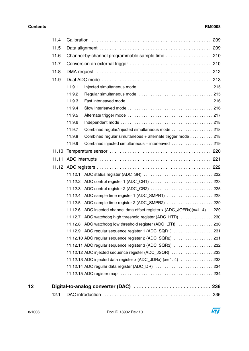
11.4 Calibration
Figure 30. Calibration timing diagram
11.5 Data alignment
Figure 31. Right alignment of data
Figure 32. Left alignment of data
11.6 Channel-by-channel programmable sample time
11.7 Conversion on external trigger
Table 63. External trigger for regular channels for ADC1 and ADC2
Table 64. External trigger for injected channels for ADC1 and ADC2
Table 65. External trigger for regular channels for ADC3
Table 66. External trigger for injected channels for ADC3
11.8 DMA request
11.9 Dual ADC mode
Figure 33. Dual ADC block diagram(1)
11.9.1 Injected simultaneous mode
Figure 34. Injected simultaneous mode on 4 channels
11.9.2 Regular simultaneous mode
Figure 35. Regular simultaneous mode on 16 channels
11.9.3 Fast interleaved mode
Figure 36. Fast interleaved mode on 1 channel in continuous conversion mode
11.9.4 Slow interleaved mode
Figure 37. Slow interleaved mode on 1 channel
11.9.5 Alternate trigger mode
Figure 38. Alternate trigger: injected channel group of each ADC
Figure 39. Alternate trigger: 4 injected channels (each ADC) in discontinuous model
11.9.6 Independent mode
11.9.7 Combined regular/injected simultaneous mode
11.9.8 Combined regular simultaneous + alternate trigger mode
Figure 40. Alternate + Regular simultaneous
Figure 41. Case of trigger occurring during injected conversion
11.9.9 Combined injected simultaneous + interleaved
Figure 42. Interleaved single channel with injected sequence CH11, CH12
11.10 Temperature sensor
Figure 43. Temperature sensor and VREFINT channel block diagram
11.11 ADC interrupts
Table 67. ADC interrupts
11.12 ADC registers
11.12.1 ADC status register (ADC_SR)
11.12.2 ADC control register 1 (ADC_CR1)
Note: These bits are reserved in ADC2 and ADC3.
In dual mode, a change of channel configuration generates a restart that can produce a loss of synchronization. It is recommended to disable dual mode before any configuration change.
Note: An EOC or JEOC interrupt is generated only on the end of conversion of the last channel if the corresponding EOCIE or JEOCIE bit is set
Note: ADC1 analog Channel16 and Channel17 are internally connected to the temperature sensor and to VREFINT, respectively.
ADC2 analog inputs Channel16 and Channel17 are internally connected to VSS.
ADC3 analog inputs Channel9, Channel14, Channel15, Channel16 and Channel17 are connected to VSS.
11.12.3 ADC control register 2 (ADC_CR2)
Note: Only ADC1 and ADC3 can generate a DMA request.
Note: If RSTCAL is set when conversion is ongoing, additional cycles are required to clear the calibration registers.
Note: If any other bit in this register apart from ADON is changed at the same time, then conversion is not triggered. This is to prevent triggering an erroneous conversion.
11.12.4 ADC sample time register 1 (ADC_SMPR1)
Note: ADC1 analog Channel16 and Channel17 are internally connected to the temperature sensor and to VREFINT, respectively.
ADC2 analog input Channel16 and Channel17 are internally connected to VSS.
ADC3 analog inputs Channel14, Channel15, Channel16 and Channel17 are connected to VSS.
11.12.5 ADC sample time register 2 (ADC_SMPR2)
Note: ADC3 analog input Channel9 is connected to VSS.
11.12.6 ADC injected channel data offset register x (ADC_JOFRx)(x=1..4)
11.12.7 ADC watchdog high threshold register (ADC_HTR)
11.12.8 ADC watchdog low threshold register (ADC_LTR)
11.12.9 ADC regular sequence register 1 (ADC_SQR1)
11.12.10 ADC regular sequence register 2 (ADC_SQR2)
11.12.11 ADC regular sequence register 3 (ADC_SQR3)
11.12.12 ADC injected sequence register (ADC_JSQR)
Note: Unlike a regular conversion sequence, if JL[1:0] length is less than four, the channels are converted in a sequence starting from (4-JL). Example: ADC_JSQR[21:0] = 10 00011 00011 00111 00010 means that a scan conversion will convert the followi...
11.12.13 ADC injected data register x (ADC_JDRx) (x= 1..4)
11.12.14 ADC regular data register (ADC_DR)
11.12.15 ADC register map
Table 68. ADC register map and reset values
12 Digital-to-analog converter (DAC)
12.1 DAC introduction
12.2 DAC main features
Figure 44. DAC channel block diagram
Table 69. DAC pins
12.3 DAC functional description
12.3.1 DAC channel enable
12.3.2 DAC output buffer enable
12.3.3 DAC data format
Figure 45. Data registers in single DAC channel mode
Figure 46. Data registers in dual DAC channel mode
12.3.4 DAC conversion
Figure 47. Timing diagram for conversion with trigger disabled TEN = 0
12.3.5 DAC output voltage
12.3.6 DAC trigger selection
Table 70. External triggers
12.3.7 DMA request
12.3.8 Noise generation
Figure 48. DAC LFSR register calculation algorithm
Figure 49. DAC conversion (SW trigger enabled) with LFSR wave generation
12.3.9 Triangle-wave generation
Figure 50. DAC triangle wave generation
Figure 51. DAC conversion (SW trigger enabled) with triangle wave generation
12.4 Dual DAC channel conversion
12.4.1 Independent trigger without wave generation
12.4.2 Independent trigger with same LFSR generation
12.4.3 Independent trigger with different LFSR generation
12.4.4 Independent trigger with same triangle generation
12.4.5 Independent trigger with different triangle generation
12.4.6 Simultaneous software start
12.4.7 Simultaneous trigger without wave generation
12.4.8 Simultaneous trigger with same LFSR generation
12.4.9 Simultaneous trigger with different LFSR generation
12.4.10 Simultaneous trigger with same triangle generation
12.4.11 Simultaneous trigger with different triangle generation
12.5 DAC registers
12.5.1 DAC control register (DAC_CR)
12.5.2 DAC software trigger register (DAC_SWTRIGR)
12.5.3 DAC channel1 12-bit right-aligned data holding register (DAC_DHR12R1)
12.5.4 DAC channel1 12-bit left aligned data holding register (DAC_DHR12L1)
12.5.5 DAC channel1 8-bit right aligned data holding register (DAC_DHR8R1)
12.5.6 DAC channel2 12-bit right aligned data holding register (DAC_DHR12R2)
12.5.7 DAC channel2 12-bit left aligned data holding register (DAC_DHR12L2)
12.5.8 DAC channel2 8-bit right-aligned data holding register (DAC_DHR8R2)
12.5.9 Dual DAC 12-bit right-aligned data holding register (DAC_DHR12RD)
12.5.10 DUAL DAC 12-bit left aligned data holding register (DAC_DHR12LD)
12.5.11 DUAL DAC 8-bit right aligned data holding register (DAC_DHR8RD)
12.5.12 DAC channel1 data output register (DAC_DOR1)
12.5.13 DAC channel2 data output register (DAC_DOR2)
12.5.14 DAC register map
Table 71. DAC register map
13 Advanced-control timers (TIM1&TIM8)
13.1 TIM1&TIM8 introduction
13.2 TIM1&TIM8 main features
Figure 52. Advanced-control timer block diagram
13.3 TIM1&TIM8 functional description
13.3.1 Time-base unit
Figure 53. Counter timing diagram with prescaler division change from 1 to 2
Figure 54. Counter timing diagram with prescaler division change from 1 to 4
13.3.2 Counter modes
Figure 55. Counter timing diagram, internal clock divided by 1
Figure 56. Counter timing diagram, internal clock divided by 2
Figure 57. Counter timing diagram, internal clock divided by 4
Figure 58. Counter timing diagram, internal clock divided by N
Figure 59. Counter timing diagram, update event when ARPE=0 (TIMx_ARR not preloaded)
Figure 60. Counter timing diagram, update event when ARPE=1 (TIMx_ARR preloaded)
Figure 61. Counter timing diagram, internal clock divided by 1
Figure 62. Counter timing diagram, internal clock divided by 2
Figure 63. Counter timing diagram, internal clock divided by 4
Figure 64. Counter timing diagram, internal clock divided by N
Figure 65. Counter timing diagram, update event when repetition counter is not used
Figure 66. Counter timing diagram, internal clock divided by 1, TIMx_ARR = 0x6
Figure 67. Counter timing diagram, internal clock divided by 2
Figure 68. Counter timing diagram, internal clock divided by 4, TIMx_ARR=0x36
Figure 69. Counter timing diagram, internal clock divided by N
Figure 70. Counter timing diagram, update event with ARPE=1 (counter underflow)
Figure 71. Counter timing diagram, Update event with ARPE=1 (counter overflow)
13.3.3 Repetition counter
Figure 72. Update rate examples depending on mode and TIMx_RCR register settings
13.3.4 Clock selection
Figure 73. Control circuit in normal mode, internal clock divided by 1
Figure 74. TI2 external clock connection example
Figure 75. Control circuit in external clock mode 1
Figure 76. External trigger input block
Figure 77. Control circuit in external clock mode 2
13.3.5 Capture/compare channels
Figure 78. Capture/compare channel (example: channel 1 input stage)
Figure 79. Capture/compare channel 1 main circuit
Figure 80. Output stage of capture/compare channel (channel 1 to 3)
Figure 81. Output stage of capture/compare channel (channel 4)
13.3.6 Input capture mode
13.3.7 PWM input mode
Figure 82. PWM input mode timing
13.3.8 Forced output mode
13.3.9 Output compare mode
Figure 83. Output compare mode, toggle on OC1.
13.3.10 PWM mode
Figure 84. Edge-aligned PWM waveforms (ARR=8)
Figure 85. Center-aligned PWM waveforms (ARR=8)
13.3.11 Complementary outputs and dead-time insertion
Figure 86. Complementary output with dead-time insertion.
Figure 87. Dead-time waveforms with delay greater than the negative pulse.
Figure 88. Dead-time waveforms with delay greater than the positive pulse.
13.3.12 Using the break function
Figure 89. Output behavior in response to a break.
13.3.13 Clearing the OCxREF signal on an external event
Figure 90. Clearing TIMx OCxREF
13.3.14 6-step PWM generation
Figure 91. 6-step generation, COM example (OSSR=1)
13.3.15 One-pulse mode
Figure 92. Example of one pulse mode.
13.3.16 Encoder interface mode
Table 72. Counting direction versus encoder signals
Figure 93. Example of counter operation in encoder interface mode.
Figure 94. Example of encoder interface mode with TI1FP1 polarity inverted.
13.3.17 Timer input XOR function
13.3.18 Interfacing with Hall sensors
Figure 95. Example of hall sensor interface
13.3.19 TIMx and external trigger synchronization
Figure 96. Control circuit in reset mode
Figure 97. Control circuit in gated mode
Figure 98. Control circuit in trigger mode
Figure 99. Control circuit in external clock mode 2 + trigger mode
13.3.20 Timer synchronization
13.3.21 Debug mode
13.4 TIM1&TIM8 registers
13.4.1 TIM1&TIM8 control register 1 (TIMx_CR1)
13.4.2 TIM1&TIM8 control register 2 (TIMx_CR2)
13.4.3 TIM1&TIM8 slave mode control register (TIMx_SMCR)
Table 73. TIMx Internal trigger connection
13.4.4 TIM1&TIM8 DMA/interrupt enable register (TIMx_DIER)
13.4.5 TIM1&TIM8 status register (TIMx_SR)
13.4.6 TIM1&TIM8 event generation register (TIMx_EGR)
13.4.7 TIM1&TIM8 capture/compare mode register 1 (TIMx_CCMR1)
13.4.8 TIM1&TIM8 capture/compare mode register 2 (TIMx_CCMR2)
13.4.9 TIM1&TIM8 capture/compare enable register (TIMx_CCER)
Table 74. Output control bits for complementary OCx and OCxN channels with break feature
13.4.10 TIM1&TIM8 counter (TIMx_CNT)
13.4.11 TIM1&TIM8 prescaler (TIMx_PSC)
13.4.12 TIM1&TIM8 auto-reload register (TIMx_ARR)
13.4.13 TIM1&TIM8 repetition counter register (TIMx_RCR)
13.4.14 TIM1&TIM8 capture/compare register 1 (TIMx_CCR1)
13.4.15 TIM1&TIM8 capture/compare register 2 (TIMx_CCR2)
13.4.16 TIM1&TIM8 capture/compare register 3 (TIMx_CCR3)
13.4.17 TIM1&TIM8 capture/compare register 4 (TIMx_CCR4)
13.4.18 TIM1&TIM8 break and dead-time register (TIMx_BDTR)
13.4.19 TIM1&TIM8 DMA control register (TIMx_DCR)
13.4.20 TIM1&TIM8 DMA address for full transfer (TIMx_DMAR)
13.4.21 TIM1&TIM8 register map
Table 75. TIM1&TIM8 register map and reset values
14 General-purpose timer (TIMx)
14.1 TIMx introduction
14.2 TIMx main features
Figure 100. General-purpose timer block diagram
14.3 TIMx functional description
14.3.1 Time-base unit
Figure 101. Counter timing diagram with prescaler division change from 1 to 2
Figure 102. Counter timing diagram with prescaler division change from 1 to 4
14.3.2 Counter modes
Figure 103. Counter timing diagram, internal clock divided by 1
Figure 104. Counter timing diagram, internal clock divided by 2
Figure 105. Counter timing diagram, internal clock divided by 4
Figure 106. Counter timing diagram, internal clock divided by N
Figure 107. Counter timing diagram, Update event when ARPE=0 (TIMx_ARR not preloaded)
Figure 108. Counter timing diagram, Update event when ARPE=1 (TIMx_ARR preloaded)
Figure 109. Counter timing diagram, internal clock divided by 1
Figure 110. Counter timing diagram, internal clock divided by 2
Figure 111. Counter timing diagram, internal clock divided by 4
Figure 112. Counter timing diagram, internal clock divided by N
Figure 113. Counter timing diagram, Update event when repetition counter is not used
Figure 114. Counter timing diagram, internal clock divided by 1, TIMx_ARR=0x6
Figure 115. Counter timing diagram, internal clock divided by 2
Figure 116. Counter timing diagram, internal clock divided by 4, TIMx_ARR=0x36
Figure 117. Counter timing diagram, internal clock divided by N
Figure 118. Counter timing diagram, Update event with ARPE=1 (counter underflow)
Figure 119. Counter timing diagram, Update event with ARPE=1 (counter overflow)
14.3.3 Clock selection
Figure 120. Control circuit in normal mode, internal clock divided by 1
Figure 121. TI2 external clock connection example
Figure 122. Control circuit in external clock mode 1
Figure 123. External trigger input block
Figure 124. Control circuit in external clock mode 2
14.3.4 Capture/compare channels
Figure 125. Capture/compare channel (example: channel 1 input stage)
Figure 126. Capture/compare channel 1 main circuit
Figure 127. Output stage of capture/compare channel (channel 1)
14.3.5 Input capture mode
14.3.6 PWM input mode
Figure 128. PWM input mode timing
14.3.7 Forced output mode
14.3.8 Output compare mode
Figure 129. Output compare mode, toggle on OC1.
14.3.9 PWM mode
Figure 130. Edge-aligned PWM waveforms (ARR=8)
Figure 131. Center-aligned PWM waveforms (ARR=8)
14.3.10 One-pulse mode
Figure 132. Example of one-pulse mode.
14.3.11 Clearing the OCxREF signal on an external event
Figure 133. Clearing TIMx OCxREF
14.3.12 Encoder interface mode
Table 76. Counting direction versus encoder signals
Figure 134. Example of counter operation in encoder interface mode.
Figure 135. Example of encoder interface mode with IC1FP1 polarity inverted.
14.3.13 Timer input XOR function
14.3.14 Timers and external trigger synchronization
Figure 136. Control circuit in reset mode
Figure 137. Control circuit in gated mode
Figure 138. Control circuit in trigger mode
Figure 139. Control circuit in external clock mode 2 + trigger mode
14.3.15 Timer synchronization
Figure 140. Master/Slave timer example
Figure 141. Gating timer 2 with OC1REF of timer 1
Figure 142. Gating timer 2 with Enable of timer 1
Figure 143. Triggering timer 2 with update of timer 1
Figure 144. Triggering timer 2 with Enable of timer 1
Figure 145. Triggering timer 1 and 2 with timer 1 TI1 input
14.3.16 Debug mode
14.4 TIMx registers
14.4.1 TIMx control register 1 (TIMx_CR1)
Note: It is not allowed to switch from edge-aligned mode to center-aligned mode as long as the counter is enabled (CEN=1)
Note: This bit is read only when the timer is configured in Center-aligned mode or Encoder mode.
Note: External clock, gated mode and encoder mode can work only if the CEN bit has been previously set by software. However trigger mode can set the CEN bit automatically by hardware.
14.4.2 TIMx control register 2 (TIMx_CR2)
14.4.3 TIMx slave mode control register (TIMx_SMCR)
Note: These bits must be changed only when they are not used (e.g. when SMS=000) to avoid wrong edge detections at the transition.
Note: The gated mode must not be used if TI1F_ED is selected as the trigger input (TS=100). Indeed, TI1F_ED outputs 1 pulse for each transition on TI1F, whereas the gated mode checks the level of the trigger signal.
Table 77. TIMx Internal trigger connection
14.4.4 TIMx DMA/Interrupt enable register (TIMx_DIER)
14.4.5 TIMx status register (TIMx_SR)
14.4.6 TIMx event generation register (TIMx_EGR)
14.4.7 TIMx capture/compare mode register 1 (TIMx_CCMR1)
Note: CC2S bits are writable only when the channel is OFF (CC2E = 0 in TIMx_CCER).
Note: 1: These bits can not be modified as long as LOCK level 3 has been programmed (LOCK bits in TIMx_BDTR register) and CC1S=00 (the channel is configured in output).
2: In PWM mode 1 or 2, the OCREF level changes only when the result of the comparison changes or when the output compare mode switches from “frozen” mode to “PWM” mode.
Note: 1: These bits can not be modified as long as LOCK level 3 has been programmed (LOCK bits in TIMx_BDTR register) and CC1S=00 (the channel is configured in output).
2: The PWM mode can be used without validating the preload register only in one- pulse mode (OPM bit set in TIMx_CR1 register). Else the behavior is not guaranteed.
Note: CC1S bits are writable only when the channel is OFF (CC1E = 0 in TIMx_CCER).
Note: CC2S bits are writable only when the channel is OFF (CC2E = 0 in TIMx_CCER).
Note: In current silicon revision, fDTS is replaced in the formula by CK_INT when ICxF[3:0]= 1, 2 or 3.
Note: CC1S bits are writable only when the channel is OFF (CC1E = 0 in TIMx_CCER).
14.4.8 Capture/compare mode register 2 (TIMx_CCMR2)
Note: CC4S bits are writable only when the channel is OFF (CC4E = 0 in TIMx_CCER).
Note: CC3S bits are writable only when the channel is OFF (CC3E = 0 in TIMx_CCER).
Note: CC4S bits are writable only when the channel is OFF (CC4E = 0 in TIMx_CCER).
Note: CC3S bits are writable only when the channel is OFF (CC3E = 0 in TIMx_CCER).
14.4.9 TIMx capture/compare enable register (TIMx_CCER)
Table 78. Output control bit for standard OCx channels
14.4.10 TIMx counter (TIMx_CNT)
14.4.11 TIMx prescaler (TIMx_PSC)
14.4.12 TIMx auto-reload register (TIMx_ARR)
14.4.13 TIMx capture/compare register 1 (TIMx_CCR1)
14.4.14 TIMx capture/compare register 2 (TIMx_CCR2)
14.4.15 TIMx capture/compare register 3 (TIMx_CCR3)
14.4.16 TIMx capture/compare register 4 (TIMx_CCR4)
14.4.17 TIMx DMA control register (TIMx_DCR)
14.4.18 TIMx DMA address for full transfer (TIMx_DMAR)
14.4.19 TIMx register map
Table 79. TIMx register map and reset values
15 Basic timers (TIM6&TIM7)
15.1 TIM6&TIM7 introduction
15.2 TIM6&TIM7 main features
Figure 146. Basic timer block diagram
15.3 TIM6&TIM7 functional description
15.3.1 Time-base unit
Figure 147. Counter timing diagram with prescaler division change from 1 to 2
Figure 148. Counter timing diagram with prescaler division change from 1 to 4
15.3.2 Counting mode
Figure 149. Counter timing diagram, internal clock divided by 1
Figure 150. Counter timing diagram, internal clock divided by 2
Figure 151. Counter timing diagram, internal clock divided by 4
Figure 152. Counter timing diagram, internal clock divided by N
Figure 153. Counter timing diagram, update event when ARPE = 0 (TIMx_ARR not preloaded)
Figure 154. Counter timing diagram, update event when ARPE=1 (TIMx_ARR preloaded)
15.3.3 Clock source
Figure 155. Control circuit in normal mode, internal clock divided by 1
15.3.4 Debug mode
15.4 TIM6&TIM7 registers
15.4.1 TIM6&TIM7 control register 1 (TIMx_CR1)
Note: Gated mode can work only if the CEN bit has been previously set by software. However trigger mode can set the CEN bit automatically by hardware.
15.4.2 TIM6&TIM7 control register 2 (TIMx_CR2)
15.4.3 TIM6&TIM7 DMA/Interrupt enable register (TIMx_DIER)
15.4.4 TIM6&TIM7 status register (TIMx_SR)
15.4.5 TIM6&TIM7 event generation register (TIMx_EGR)
15.4.6 TIM6&TIM7 counter (TIMx_CNT)
15.4.7 TIM6&TIM7 prescaler (TIMx_PSC)
15.4.8 TIM6&TIM7 auto-reload register (TIMx_ARR)
15.4.9 TIM6&TIM7 register map
Table 80. TIM6&TIM7 register map and reset values
16 Real-time clock (RTC)
16.1 RTC introduction
16.2 RTC main features
16.3 RTC functional description
16.3.1 Overview
Figure 156. RTC simplified block diagram
16.3.2 Resetting RTC registers
16.3.3 Reading RTC registers
16.3.4 Configuring RTC registers
16.3.5 RTC flag assertion
Figure 157. RTC second and alarm waveform example with PR=0003, ALARM=00004
Figure 158. RTC Overflow waveform example with PR=0003
16.4 RTC registers
16.4.1 RTC control register high (RTC_CRH)
16.4.2 RTC control register low (RTC_CRL)
16.4.3 RTC prescaler load register (RTC_PRLH / RTC_PRLL)
Caution: The zero value is not recommended. RTC interrupts and flags cannot be asserted correctly.
16.4.4 RTC prescaler divider register (RTC_DIVH / RTC_DIVL)
16.4.5 RTC counter register (RTC_CNTH / RTC_CNTL)
16.4.6 RTC alarm register high (RTC_ALRH / RTC_ALRL)
16.4.7 RTC register map
Table 81. RTC register map and reset values
17 Independent watchdog (IWDG)
17.1 IWDG introduction
17.2 IWDG main features
17.3 IWDG functional description
17.3.1 Hardware watchdog
17.3.2 Register access protection
17.3.3 Debug mode
Figure 159. Independent watchdog block diagram
Table 82. Min/max IWDG timeout period at 40 kHz (LSI)
17.4 IWDG registers
17.4.1 Key register (IWDG_KR)
17.4.2 Prescaler register (IWDG_PR)
Note: Reading this register returns the prescaler value from the VDD voltage domain. This value may not be up to date/valid if a write operation to this register is ongoing. For this reason the value read from this register is valid only when the PVU...
17.4.3 Reload register (IWDG_RLR)
Note: Reading this register returns the reload value from the VDD voltage domain. This value may not be up to date/valid if a write operation to this register is ongoing on this register. For this reason the value read from this register is valid onl...
17.4.4 Status register (IWDG_SR)
17.4.5 IWDG register map
Table 83. IWDG register map and reset values
18 Window watchdog (WWDG)
18.1 WWDG introduction
18.2 WWDG main features
18.3 WWDG functional description
Figure 160. Watchdog block diagram
18.4 How to program the watchdog timeout
Figure 161. Window watchdog timing diagram
18.5 Debug mode
18.6 WWDG registers
18.6.1 Control register (WWDG_CR)
18.6.2 Configuration register (WWDG_CFR)
18.6.3 Status register (WWDG_SR)
18.6.4 WWDG register map
Table 84. WWDG register map and reset values
19 Flexible static memory controller (FSMC)
19.1 FSMC main features
19.2 Block diagram
19.3 AHB interface
19.3.1 Supported memories and transactions
19.4 External device address mapping
Figure 162. FSMC memory banks
19.4.1 NOR/PSRAM address mapping
Table 85. NOR/PSRAM bank selection
Table 86. External memory address
19.4.2 NAND/PC Card address mapping
Table 87. Memory mapping and timing registers
Table 88. NAND bank selections
19.5 NOR Flash/PSRAM controller
Table 89. Programmable NOR/PSRAM access parameters
19.5.1 External memory interface signals
Table 90. Nonmuxed I/O NOR Flash
Table 91. Muxed I/O NOR Flash
Table 92. Non muxed I/Os PSRAM
19.5.2 Supported memories and transactions
Table 93. NOR Flash/PSRAM supported memories and transactions
19.5.3 General timing rules
19.5.4 NOR Flash/PSRAM controller timing diagrams
Figure 163. Mode1 read accesses
Table 94. FSMC_BCRx bit fields
Table 95. FSMC_BTRx bit fields
Figure 164. ModeA read accesses
Figure 165. ModeA write accesses
Table 96. FSMC_BCRx bit fields
Table 97. FSMC_BTRx bit fields
Table 98. FSMC_BWTRx bit fields
Figure 166. Mode2/B read accesses
Figure 167. Mode2 write accesses
Figure 168. ModeB write accesses
Table 99. FSMC_BCRx bit fields
Table 100. FSMC_BTRx bit fields
Table 101. FSMC_BWTRx bit fields
Figure 169. ModeC read accesses
Figure 170. ModeC write accesses
Table 102. FSMC_BCRx bit fields
Table 103. FSMC_BTRx bit fields
Table 104. FSMC_BWTRx bit fields
Figure 171. ModeD read accesses
Table 105. FSMC_BCRx bit fields
Table 106. FSMC_BTRx bit fields
Table 107. FSMC_BWTRx bit fields
Figure 172. Muxed read accesses
Figure 173. Muxed write accesses
Table 108. FSMC_BCRx bit fields
Table 109. FSMC_BTRx bit fields
19.5.5 Synchronous burst transactions
Figure 174. Synchronous multiplexed read mode - NOR, PSRAM (CRAM)
Table 110. FSMC_BCRx bit fields
Table 111. FSMC_BTRx bit fields
Figure 175. Synchronous multiplexed write mode - PSRAM (CRAM)
Table 112. FSMC_BCRx bit fields
Table 113. FSMC_BTRx bit fields
19.5.6 NOR/PSRAM controller registers
19.6 NAND Flash/PC Card controller
Table 114. Programmable NAND/PC Card access parameters
19.6.1 External memory interface signals
Table 115. 8-bit NAND Flash
Table 116. 16-bit NAND Flash
Table 117. 16-bit PC Card
19.6.2 NAND Flash / PC Card supported memories and transactions
Table 118. Supported memories and transactions
19.6.3 Timing diagrams for NAND, ATA and PC Card
Figure 176. NAND/PC Card controller timing for common memory access
19.6.4 NAND Flash operations
19.6.5 NAND Flash pre-wait functionality
Figure 177. Access to non ‘CE don’t care’ NAND-Flash
19.6.6 Error correction code computation ECC (NAND Flash)
19.6.7 NAND Flash/PC Card controller registers
Table 119. ECC result relevant bits
19.6.8 FSMC register map
Table 120. FSMC register map
20 Secure digital input/output interface (SDIO)
20.1 SDIO main features
20.2 SDIO bus topology
Figure 178. SDIO “no response” and “no data” operations
Figure 179. SDIO (multiple) block read operation
Figure 180. SDIO (multiple) block write operation
Figure 181. SDIO sequential read operation
Figure 182. SDIO sequential write operation
20.3 SDIO functional description
Figure 183. SDIO block diagram
Table 121. SDIO I/O definitions
20.3.1 SDIO adapter
Figure 184. SDIO adapter
Figure 185. Control unit
Figure 186. SDIO adapter command path
Figure 187. Command path state machine (CPSM)
Figure 188. SDIO command transfer
Table 122. Command format
Table 123. Short response format
Table 124. Long response format
Table 125. Command path status flags
Figure 189. Data path
Figure 190. Data path state machine (DPSM)
Table 126. Data token format
Table 127. Transmit FIFO status flags
Table 128. Receive FIFO status flags
20.3.2 SDIO AHB interface
20.4 Card functional description
20.4.1 Card identification mode
20.4.2 Card reset
20.4.3 Operating voltage range validation
20.4.4 Card identification process
20.4.5 Block write
20.4.6 Block read
20.4.7 Stream access, stream write and stream read (MultiMediaCard only)
20.4.8 Erase: group erase and sector erase
20.4.9 Wide bus selection or deselection
20.4.10 Protection management
20.4.11 Card status register
Table 129. Card status
20.4.12 SD status register
Table 130. SD status
Table 131. Speed class code field
Table 132. Performance move field
Table 133. AU_SIZE field
Table 134. Maximum AU size
Table 135. Erase size field
Table 136. Erase timeout field
Table 137. Erase offset field
20.4.13 SD I/O mode
20.4.14 Commands and responses
Table 138. Block-oriented write commands
Table 139. Block-oriented write protection commands
Table 140. Erase commands
Table 141. I/O mode commands
Table 142. Lock card
Table 143. Application-specific commands
20.5 Response formats
20.5.1 R1 (normal response command)
Table 144. R1 response
20.5.2 R1b
20.5.3 R2 (CID, CSD register)
Table 145. R2 response
20.5.4 R3 (OCR register)
Table 146. R3 response
20.5.5 R4 (Fast I/O)
Table 147. R4 response
20.5.6 R4b
Table 148. R4b response
20.5.7 R5 (interrupt request)
Table 149. R5 response
20.5.8 R6
Table 150. R6 response
20.6 SDIO I/O card-specific operations
20.6.1 SDIO I/O read wait operation by SDIO_D2 signalling
20.6.2 SDIO read wait operation by stopping SDIO_CK
20.6.3 SDIO suspend/resume operation
20.6.4 SDIO interrupts
20.7 CE-ATA specific operations
20.7.1 Command completion signal disable
20.7.2 Command completion signal enable
20.7.3 CE-ATA interrupt
20.7.4 Aborting CMD61
20.8 HW flow control
20.9 SDIO registers
20.9.1 SDIO power control register (SDIO_POWER)
20.9.2 SDI clock control register (SDIO_CLKCR)
20.9.3 SDIO argument register (SDIO_ARG)
20.9.4 SDIO command register (SDIO_CMD)
20.9.5 SDIO command response register (SDIO_RESPCMD)
20.9.6 SDIO response 1..4 register (SDIO_RESPx)
Table 151. Response type and SDIO_RESPx registers
20.9.7 SDIO data timer register (SDIO_DTIMER)
20.9.8 SDIO data length register (SDIO_DLEN)
20.9.9 SDIO data control register (SDIO_DCTRL)
20.9.10 SDIO data counter register (SDIO_DCOUNT)
20.9.11 SDIO status register (SDIO_STA)
20.9.12 SDIO interrupt clear register (SDIO_ICR)
20.9.13 SDIO mask register (SDIO_MASK)
20.9.14 SDIO FIFO counter register (SDIO_FIFOCNT)
20.9.15 SDIO data FIFO register (SDIO_FIFO)
20.9.16 SDIO register map
Table 152. SDIO register map
21 Universal serial bus full-speed device interface (USB)
21.1 USB introduction
21.2 USB main features
21.3 USB functional description
Figure 191. USB peripheral block diagram
21.3.1 Description of USB blocks
21.4 Programming considerations
21.4.1 Generic USB device programming
21.4.2 System and power-on reset
Figure 192. Packet buffer areas with examples of buffer description table locations
21.4.3 Double-buffered endpoints
Table 153. Double-buffering buffer flag definition
Table 154. Bulk double-buffering memory buffers usage
21.4.4 Isochronous transfers
Table 155. Isochronous memory buffers usage
21.4.5 Suspend/Resume events
Table 156. Resume event detection
21.5 USB registers
21.5.1 Common registers
21.5.2 Endpoint-specific registers
Table 157. Reception status encoding
Table 158. Endpoint type encoding
Table 159. Endpoint kind meaning
Table 160. Transmission status encoding
21.5.3 Buffer descriptor table
Table 161. Definition of allocated buffer memory
21.5.4 USB register map
Table 162. USB register map and reset values
22 Controller area network (bxCAN)
22.1 bxCAN introduction
22.2 bxCAN main features
22.3 bxCAN general description
Figure 193. CAN network topology
22.3.1 CAN 2.0B active core
22.3.2 Control, status and configuration registers
22.3.3 Tx mailboxes
22.3.4 Acceptance filters
Figure 194. Dual CAN block diagram (connectivity devices)
22.4 bxCAN operating modes
22.4.1 Initialization mode
22.4.2 Normal mode
22.4.3 Sleep mode (low power)
Figure 195. bxCAN operating modes
22.5 Test mode
22.5.1 Silent mode
Figure 196. bxCAN in silent mode
22.5.2 Loop back mode
Figure 197. bxCAN in loop back mode
22.5.3 Loop back combined with silent mode
Figure 198. bxCAN in combined mode
22.6 STM32F10xxx in Debug mode
22.7 bxCAN functional description
22.7.1 Transmission handling
Figure 199. Transmit mailbox states
22.7.2 Time triggered communication mode
22.7.3 Reception handling
Figure 200. Receive FIFO states
22.7.4 Identifier filtering
Figure 201. Filter bank scale configuration - register organization
Figure 202. Example of filter numbering
Figure 203. Filtering mechanism - example
22.7.5 Message storage
Table 163. Transmit mailbox mapping
Table 164. Receive mailbox mapping
Figure 204. CAN error state diagram
22.7.6 Error management
22.7.7 Bit timing
Figure 205. Bit timing
Figure 206. CAN frames
22.8 bxCAN interrupts
Figure 207. Event flags and interrupt generation
22.9 CAN registers
22.9.1 Register access protection
22.9.2 CAN control and status registers
22.9.3 CAN mailbox registers
22.9.4 CAN filter registers
22.9.5 bxCAN register map
Table 165. bxCAN register map and reset values
23 Serial peripheral interface (SPI)
23.1 SPI introduction
23.2 SPI and I2S main features
23.2.1 SPI features
23.2.2 I2S features
23.3 SPI functional description
23.3.1 General description
Figure 208. SPI block diagram
Figure 209. Single master/ single slave application
Figure 210. Hardware/software slave select management
Figure 211. Data clock timing diagram
23.3.2 Configuring the SPI in slave mode
23.3.3 Configuring the SPI in master mode
23.3.4 Configuring the SPI for Simplex communication
23.3.5 Data transmission and reception procedures
Figure 212. TXE/RXNE/BSY behavior in Master / full-duplex mode (BIDIMODE=0 and RXONLY=0) in the case of continuous transfers
Figure 213. TXE/RXNE/BSY behavior in Slave / full-duplex mode (BIDIMODE=0, RXONLY=0) in the case of continuous transfers
Figure 214. TXE/BSY behavior in Master transmit-only mode (BIDIMODE=0 and RXONLY=0) in the case of continuous transfers
Figure 215. TXE/BSY in Slave transmit-only mode (BIDIMODE=0 and RXONLY=0) in the case of continuous transfers
Figure 216. RXNE behavior in receive-only mode (BIDIRMODE=0 and RXONLY=1) in the case of continuous transfers
Figure 217. TXE/BSY behavior when transmitting (BIDIRMODE=0 and RXONLY=0) in the case of discontinuous transfers
23.3.6 CRC calculation
23.3.7 Status flags
23.3.8 Disabling the SPI
23.3.9 SPI communication using DMA (direct memory addressing)
Figure 218. Transmission using DMA
Figure 219. Reception using DMA
23.3.10 Error flags
23.3.11 SPI interrupts
Table 166. SPI interrupt requests
23.4 I2S functional description
23.4.1 I2S general description
Figure 220. I2S block diagram
23.4.2 Supported audio protocols
Figure 221. I2S Phillips protocol waveforms (16/32-bit full accuracy, CPOL = 0)
Figure 222. I2S Phillips standard waveforms (24-bit frame with CPOL = 0)
Figure 223. Transmitting 0x8EAA33
Figure 224. Receiving 0x8EAA33
Figure 225. I2S Phillips standard (16-bit extended to 32-bit packet frame with CPOL = 0)
Figure 226. Example
Figure 227. MSB Justified 16-bit or 32-bit full-accuracy length with CPOL = 0
Figure 228. MSB Justified 24-bit frame length with CPOL = 0
Figure 229. MSB Justified 16-bit extended to 32-bit packet frame with CPOL = 0
Figure 230. LSB justified 16-bit or 32-bit full-accuracy with CPOL = 0
Figure 231. LSB Justified 24-bit frame length with CPOL = 0
Figure 232. Operations required to transmit 0x3478AE
Figure 233. Operations required to receive 0x3478AE
Figure 234. LSB Justified 16-bit extended to 32-bit packet frame with CPOL = 0
Figure 235. Example
Figure 236. PCM standard waveforms (16-bit)
Figure 237. PCM standard waveforms (16-bit extended to 32-bit packet frame)
23.4.3 Clock generator
Figure 238. Audio sampling frequency definition
Figure 239. I2S clock generator architecture
Table 167. Audio-frequency precision using standard 8 MHz HSE (high-density devices only)
Table 168. Audio-frequency precision using standard 25 MHz and PLL3 (connectivity line devices only)
Table 169. Audio-frequency precision using standard 14.7456 MHz and PLL3 (connectivity line devices only)
23.4.4 I2S master mode
23.4.5 I2S slave mode
23.4.6 Status flags
23.4.7 Error flags
23.4.8 I2S interrupts
Table 170. I2S interrupt requests
23.4.9 DMA features
23.5 SPI and I2S registers
23.5.1 SPI control register 1 (SPI_CR1) (not used in I2S mode)
Note: Not used in I2S mode
Note: In master mode, the MOSI pin is used and in slave mode, the MISO pin is used.
Not used in I2S mode
Note: This bit should be written only when SPI is disabled (SPE = ‘0’) for correct operation
Not used in I2S mode
Note: This bit has to be written as soon as the last data is written into the SPI_DR register.
Not used in I2S mode
Note: This bit should be written only when SPI is disabled (SPE = ‘0’) for correct operation
Not used in I2S mode
Note: Not used in I2S mode
Note: Not used in I2S mode
Note: Not used in I2S mode
Note: This bit should not be changed when communication is ongoing.
Not used in I2S mode
Note: 1- Not used in I2S mode.
Note: 2- When disabling the SPI, follow the procedure described in Section 23.3.8: Disabling the SPI.
Note: These bits should not be changed when communication is ongoing.
Not used in I2S mode
Note: This bit should not be changed when communication is ongoing.
Not used in I2S mode
Note: This bit should not be changed when communication is ongoing.
Not used in I2S mode
Note: This bit should not be changed when communication is ongoing.
Note: Not used in I2S mode
23.5.2 SPI control register 2 (SPI_CR2)
Note: Not used in I2S mode
23.5.3 SPI status register (SPI_SR)
Note: BSY flag must be used with caution: refer to Section 23.3.7: Status flags and Section 23.3.8: Disabling the SPI.
Note: Not used in I2S mode
Note: Not used in I2S mode
Note: Not used in SPI mode
Note: Not used for the SPI mode. No meaning in PCM mode
23.5.4 SPI data register (SPI_DR)
Depending on the data frame format selection bit (DFF in SPI_CR1 register), the data sent or received is either 8-bit or 16-bit. This selection has to be made before enabling the SPI to ensure correct operation.
For an 8-bit data frame, the buffers are 8-bit and only the LSB of the register (SPI_DR[7:0]) is used for transmission/reception. When in reception mode, the MSB of the register (SPI_DR[15:8]) is forced to 0.
For a 16-bit data frame, the buffers are 16-bit and the entire register, SPI_DR[15:0] is used for transmission/reception.
23.5.5 SPI CRC polynomial register (SPI_CRCPR) (not used in I2S mode)
Note: Not used for the I2S mode.
23.5.6 SPI Rx CRC register (SPI_RXCRCR) (not used in I2S mode)
Note: A read to this register when the BSY Flag is set could return an incorrect value. Not used for the I2S mode.
23.5.7 SPI Tx CRC register (SPI_TXCRCR) (not used in I2S mode)
Note: A read to this register when the BSY flag is set could return an incorrect value. Not used for the I2S mode.
23.5.8 SPI_I2S configuration register (SPI_I2SCFGR)
Note: This bit should be configured when the SPI or I2S is disabled
Note: Not used in SPI mode
Note: This bit should be configured when the I2S is disabled.
Not used for the SPI mode
Note: This bit has a meaning only if I2SSTD = 11 (PCM standard is used)
Not used for the SPI mode
Note: For correct operation, these bits should be configured when the I2S is disabled.
Not used in SPI mode
Note: For correct operation, this bit should be configured when the I2S is disabled.
Not used in SPI mode
Note: For correct operation, these bits should be configured when the I2S is disabled.
Not used in SPI mode
Note: For correct operation, this bit should be configured when the I2S is disabled.
Not used in SPI mode
23.5.9 SPI_I2S prescaler register (SPI_I2SPR)
Note: This bit should be configured when the I2S is disabled. It is used only when the I2S is in master mode.
Not used in SPI mode.
Note: This bit should be configured when the I2S is disabled. It is used only when the I2S is in master mode.
Not used in SPI mode
Note: These bits should be configured when the I2S is disabled. It is used only when the I2S is in master mode.
Not used in SPI mode.
23.5.10 SPI register map
Table 171. SPI register map and reset values
24 Inter-integrated circuit (I2C) interface
24.1 I2C introduction
24.2 I2C main features
24.3 I2C functional description
24.3.1 Mode selection
Figure 240. I2C bus protocol
Figure 241. I2C block diagram
24.3.2 I2C slave mode
Figure 242. Transfer sequence diagram for slave transmitter
Figure 243. Transfer sequence diagram for slave receiver
24.3.3 I2C master mode
Figure 244. Transfer sequence diagram for master transmitter
Figure 245. Transfer sequence diagram for master receiver
24.3.4 Error conditions
24.3.5 SDA/SCL line control
24.3.6 SMBus
Table 172. SMBus vs. I2C
24.3.7 DMA requests
24.3.8 Packet error checking
24.4 I2C interrupts
Table 173. I2C Interrupt requests
Figure 246. I2C interrupt mapping diagram
24.5 I2C debug mode
24.6 I2C registers
24.6.1 Control register 1 (I2C_CR1)
Note: This bit can be used in case the BUSY bit is set to ‘1 when no stop condition has been detected on the bus.
Note: PEC calculation is corrupted by an arbitration loss.
Note: The POS bit must be used only in 2-byte reception configuration and must be configured before data reception starts. To NACK the 2nd byte, the ACK bit must be cleared after ADDR is cleared. To check the 2nd byte as PEC, the PEC bit must be set ...
Note: When the STOP, START or PEC bit is set, the software must not perform any write access to I2C_CR1 before this bit is cleared by hardware. Otherwise there is a risk of setting a second STOP, START or PEC request.
Note: If this bit is reset while a communication is on going, the peripheral is disabled at the end of the current communication, when back to IDLE state. All bit resets due to PE=0 occur at the end of the communication.
In master mode, this bit must not be reset before the end of the communication.
24.6.2 Control register 2 (I2C_CR2)
Note: This bit is used in master receiver mode to permit the generation of a NACK on the last received data.
24.6.3 Own address register 1 (I2C_OAR1)
24.6.4 Own address register 2 (I2C_OAR2)
24.6.5 Data register (I2C_DR)
Note: In slave mode, the address is not copied into DR.
Note: Write collision is not managed (DR can be written if TxE=0).
Note: If an ARLO event occurs on ACK pulse, the received byte is not copied into DR and so cannot be read.
24.6.6 Status register 1 (I2C_SR1)
Note: If the DR write occurs very close to SCL rising edge, the sent data is unspecified and a hold timing error occurs
Note: In SMBUS, the arbitration on the data in slave mode occurs only during the data phase, or the acknowledge transmission (not on the address acknowledge).
Note: TxE is not cleared by writing the first data being transmitted, or by writing data when BTF is set, as in both cases the data register is still empty.
Note: RxNE is not cleared by reading data when BTF is set, as the data register is still full.
Note: The STOPF bit is not set after a NACK reception
Note: ADD10 bit is not set after a NACK reception
Note: The BTF bit is not set after a NACK reception
The BTF bit is not set if next byte to be transmitted is the PEC (TRA=1 in I2C_SR2 register and PEC=1 in I2C_CR1 register)
Note: ADDR is not set after a NACK reception
24.6.7 Status register 2 (I2C_SR2)
24.6.8 Clock control register (I2C_CCR)
Note: 1. The minimum allowed value is 0x04, except in FAST DUTY mode where the minimum allowed value is 0x01 2. thigh = tr(SCL) + tw(SCLH). See device datasheet for the definitions of parameters 3. tlow = tf(SCL) + tw(SCLL). See device datasheet for ...
24.6.9 TRISE register (I2C_TRISE)
Note: TRISE[5:0] must be configured only when the I2C is disabled (PE = 0).
24.6.10 I2C register map
Table 174. I2C register map and reset values
25 Universal synchronous asynchronous receiver transmitter (USART)
25.1 USART introduction
25.2 USART main features
25.3 USART functional description
Figure 247. USART block diagram
25.3.1 USART character description
Figure 248. Word length programming
25.3.2 Transmitter
Figure 249. Configurable stop bits
Figure 250. TC/TXE behavior when transmitting
25.3.3 Receiver
Figure 251. Start bit detection
Figure 252. Data sampling for noise detection
Table 175. Noise detection from sampled data
25.3.4 Fractional baud rate generation
Table 176. Error calculation for programmed baud rates
25.3.5 USART receiver’s tolerance to clock deviation
Table 177. USART receiver ‘s tolerance when DIV_Fraction is 0
Table 178. USART receiver’s tolerance when DIV_Fraction is different from 0
25.3.6 Multiprocessor communication
Figure 253. Mute mode using Idle line detection
Figure 254. Mute mode using Address mark detection
25.3.7 Parity control
Table 179. Frame formats
25.3.8 LIN (local interconnection network) mode
Figure 255. Break detection in LIN mode (11-bit break length - LBDL bit is set)
Figure 256. Break detection in LIN mode vs. Framing error detection
25.3.9 USART synchronous mode
Figure 257. USART example of synchronous transmission
Figure 258. USART data clock timing diagram (M=0)
Figure 259. USART data clock timing diagram (M=1)
Figure 260. RX data setup/hold time
25.3.10 Single-wire half-duplex communication
25.3.11 Smartcard
Figure 261. ISO 7816-3 asynchronous protocol
Figure 262. Parity error detection using the 1.5 stop bits
25.3.12 IrDA SIR ENDEC block
Figure 263. IrDA SIR ENDEC- block diagram
Figure 264. IrDA data modulation (3/16) -normal mode
25.3.13 Continuous communication using DMA
Figure 265. Transmission using DMA
Figure 266. Reception using DMA
25.3.14 Hardware flow control
Figure 267. Hardware flow control between 2 USART
Figure 268. RTS flow control
Figure 269. CTS flow control
25.4 USART interrupts
Table 180. USART interrupt requests
Figure 270. USART interrupt mapping diagram
25.5 USART mode configuration
Table 181. USART mode configuration
25.6 USART registers
25.6.1 Status register (USART_SR)
Note: This bit is not available for UART4 & UART5.
Note: An interrupt is generated when LBD=1 if LBDIE=1
Note: This bit is used during single buffer transmission.
Note: The IDLE bit will not be set again until the RXNE bit has been set itself (i.e. a new idle line occurs).
Note: When this bit is set, the RDR register content will not be lost but the shift register will be overwritten. An interrupt is generated on ORE flag in case of Multi Buffer communication if the EIE bit is set.
Note: This bit does not generate interrupt as it appears at the same time as the RXNE bit which itself generates an interrupting interrupt is generated on NE flag in case of Multi Buffer communication if the EIE bit is set.
Note: This bit does not generate interrupt as it appears at the same time as the RXNE bit which itself generates an interrupt. If the word currently being transferred causes both frame error and overrun error, it will be transferred and only the ORE ...
An interrupt is generated on FE flag in case of Multi Buffer communication if the EIE bit is set.
25.6.2 Data register (USART_DR)
25.6.3 Baud rate register (USART_BRR)
25.6.4 Control register 1 (USART_CR1)
Note: The M bit must not be modified during a data transfer (both transmission and reception)
Note: 1: During transmission, a “0” pulse on the TE bit (“0” followed by “1”) sends a preamble (idle line) after the current word, except in smartcard mode.
2: When TE is set there is a 1 bit-time delay before the transmission starts.
Note: 1: Before selecting Mute mode (by setting the RWU bit) the USART must first receive a data byte, otherwise it cannot function in Mute mode with wakeup by Idle line detection.
2: In Address Mark Detection wakeup configuration (WAKE bit=1) the RWU bit cannot be modified by software while the RXNE bit is set.
25.6.5 Control register 2 (USART_CR2)
Note: The 0.5 Stop bit and 1.5 Stop bit are not available for UART4 & UART5.
Note: This bit is not available for UART4 & UART5.
Note: This bit is not available for UART4 & UART5.
Note: This bit is not available for UART4 & UART5.
Note: 1: The last bit is the 8th or 9th data bit transmitted depending on the 8 or 9 bit format selected by the M bit in the USART_CR1 register.
2: This bit is not available for UART4 & UART5.
25.6.6 Control register 3 (USART_CR3)
Note: This bit is not available for UART4 & UART5.
Note: This bit is not available for UART4 & UART5.
Note: This bit is not available for UART4 & UART5.
Note: This bit is not available for UART5.
Note: This bit is not available for UART5.
Note: This bit is not available for UART4 & UART5.
Note: This bit is not available for UART4 & UART5.
25.6.7 Guard time and prescaler register (USART_GTPR)
Note: This bit is not available for UART4 & UART5.
Note: 1: Bits [7:5] have no effect if Smartcard mode is used. 2: This bit is not available for UART4 & UART5.
25.6.8 USART register map
Table 182. USART register map and reset values
26 USB on-the-go full-speed (OTG_FS)
26.1 OTG_FS introduction
26.2 OTG_FS main features
26.2.1 General features
26.2.2 Host-mode features
26.2.3 Peripheral-mode features
26.3 OTG_FS functional description
Figure 271. Block diagram
26.3.1 OTG full-speed core
26.3.2 Full-speed OTG PHY
26.4 OTG dual role device (DRD)
Figure 272. OTG A-B device connection
26.4.1 ID line detection
26.4.2 HNP dual role device
26.4.3 SRP dual role device
26.5 USB peripheral
Figure 273. USB peripheral-only connection
26.5.1 SRP-capable peripheral
26.5.2 Peripheral states
26.5.3 Peripheral endpoints
26.6 USB host
Figure 274. USB host-only connection
26.6.1 SRP-capable host
26.6.2 USB host states
26.6.3 Host channels
26.6.4 Host scheduler
26.7 SOF trigger
Figure 275. SOF connectivity
26.7.1 Host SOFs
26.7.2 Peripheral SOFs
26.8 Power options
26.9 USB data FIFOs
Figure 276. OTG_FS controller block diagram
26.10 Peripheral FIFO architecture
Figure 277. Device-mode FIFO address mapping and AHB FIFO access mapping
26.10.1 Peripheral Rx FIFO
26.10.2 Peripheral Tx FIFOs
26.11 Host FIFO architecture
Figure 278. Host-mode FIFO address mapping and AHB FIFO access mapping
26.11.1 Host Rx FIFO
26.11.2 Host Tx FIFOs
26.12 USB system performance
26.13 OTG_FS interrupts
Figure 279. Interrupt hierarchy
26.14 OTG_FS control and status registers
26.14.1 CSR memory map
Figure 280. CSR memory map
Table 183. Core global control and status registers (CSRs)
Table 184. Host-mode control and status registers (CSRs)
Table 185. Device-mode control and status registers
Table 186. Data FIFO (DFIFO) access register map
Table 187. Power and clock gating control and status registers
26.14.2 OTG_FS global registers
26.14.3 Host-mode registers
26.14.4 Device-mode registers
Table 188. Minimum duration for soft disconnect
26.14.5 OTG_FS power and clock gating control register (OTG_FS_PCGCCTL)
26.14.6 OTG_FS register map
Table 189. OTG_FS register map and reset values
26.15 OTG_FS programming model
26.15.1 Core initialization
26.15.2 Host initialization
26.15.3 Device initialization
26.15.4 Host programming model
Figure 281. Transmit FIFO write task
Figure 282. Receive FIFO read task
Figure 283. Normal bulk/control OUT/SETUP and bulk/control IN transactions
Figure 284. Bulk/control IN transactions
Figure 285. Normal interrupt OUT/IN transactions
Figure 286. Normal isochronous OUT/IN transactions
26.15.5 Device programming model
26.15.6 Operational model
Figure 287. Receive FIFO packet read in slave mode
Figure 288. Processing a SETUP packet
Figure 289. Slave mode bulk OUT transaction
26.15.7 Worst case response time
Figure 290. TRDT max timing case
26.15.8 OTG programming model
Figure 291. A-Device SRP
Figure 292. B-device SRP
Figure 293. A-device HNP
Figure 294. B-device HNP
27 Ethernet (ETH): media access control (MAC) with DMA controller
27.1 Ethernet introduction
27.2 Ethernet main features
27.2.1 MAC core features
27.2.2 DMA features
27.2.3 PTP features
27.3 Ethernet pins
Table 190. Ethernet pin configuration
27.4 Ethernet functional description: SMI, MII and RMII
Figure 295. ETH block diagram
27.4.1 Station management interface: SMI
Figure 296. SMI interface signals
Table 191. Management frame format
Figure 297. MDIO timing and frame structure - Write cycle
Figure 298. MDIO timing and frame structure - Read cycle
Table 192. Clock range
27.4.2 Media-independent interface: MII
Figure 299. Media independent interface signals
Table 193. TX interface signal encoding
Table 194. RX interface signal encoding
Figure 300. MII clock sources
27.4.3 Reduced media-independent interface: RMII
Figure 301. Reduced media-independent interface signals
Figure 302. RMII clock sources
27.4.4 MII/RMII selection
Figure 303. Clock scheme
27.5 Ethernet functional description: MAC 802.3
27.5.1 MAC 802.3 frame format
Figure 304. Address field format
Figure 305. MAC frame format
Figure 306. Tagged MAC frame format
27.5.2 MAC frame transmission
Figure 307. Transmission bit order
Figure 308. Transmission with no collision
Figure 309. Transmission with collision
Figure 310. Frame transmission in MMI and RMII modes
27.5.3 MAC frame reception
Table 195. Frame statuses
Figure 311. Receive bit order
Figure 312. Reception with no error
Figure 313. Reception with errors
Figure 314. Reception with false carrier indication
27.5.4 MAC interrupts
Figure 315. MAC core interrupt masking scheme
27.5.5 MAC filtering
Table 196. Destination address filtering table
Table 197. Source address filtering table
27.5.6 MAC loopback mode
27.5.7 MAC management counters: MMC
27.5.8 Power management: PMT
Figure 316. Wakeup frame filter register
27.5.9 Precision time protocol (IEEE1588 PTP)
Figure 317. Networked time synchronization
Figure 318. System time update using the Fine correction method
Figure 319. PTP trigger output to TIM2 ITR1 connection
Figure 320. PPS output
27.6 Ethernet functional description: DMA controller operation
Figure 321. Descriptor ring and chain structure
27.6.1 Initialization of a transfer using DMA
27.6.2 Host bus burst access
27.6.3 Host data buffer alignment
27.6.4 Buffer size calculations
27.6.5 DMA arbiter
27.6.6 Error response to DMA
27.6.7 Tx DMA configuration
Figure 322. TxDMA operation in Default mode
Figure 323. TxDMA operation in OSF mode
Figure 324. Transmit descriptor
Figure 325. Transmit descriptor field format with IEEE1588 time stamp enabled
27.6.8 Rx DMA configuration
Figure 326. Receive DMA operation
Figure 327. Rx DMA descriptor structure
Table 198. Receive descriptor 0
Figure 328. Receive descriptor fields format with IEEE1588 time stamp enabled
27.6.9 DMA interrupts
Figure 329. Interrupt scheme
27.7 Ethernet interrupts
27.8 Ethernet register descriptions
27.8.1 MAC register description
Figure 330. Ethernet MAC remote wakeup frame filter register (ETH_MACRWUFFR)
27.8.2 MMC register description
27.8.3 IEEE 1588 time stamp registers
27.8.4 DMA register description
27.8.5 Ethernet register maps
Table 199. Ethernet register map and reset values
28 Device electronic signature
28.1 Memory size registers
28.1.1 Flash size register
28.2 Unique device ID register (96 bits)
29 Debug support (DBG)
29.1 Overview
Figure 331. Block diagram of STM32F10xxx-level and Cortex-M3-level debug support
29.2 Reference ARM documentation
29.3 SWJ debug port (serial wire and JTAG)
Figure 332. SWJ debug port
29.3.1 Mechanism to select the JTAG-DP or the SW-DP
29.4 Pinout and debug port pins
29.4.1 SWJ debug port pins
Table 200. SWJ debug port pins
29.4.2 Flexible SWJ-DP pin assignment
Table 201. Flexible SWJ-DP pin assignment
29.4.3 Internal pull-up and pull-down on JTAG pins
29.4.4 Using serial wire and releasing the unused debug pins as GPIOs
29.5 STM32F10xxx JTAG TAP connection
Figure 333. JTAG TAP connections
29.6 ID codes and locking mechanism
29.6.1 MCU device ID code
29.6.2 Boundary scan TAP
29.6.3 Cortex-M3 TAP
29.6.4 Cortex-M3 JEDEC-106 ID code
29.7 JTAG debug port
Table 202. JTAG debug port data registers
Table 203. 32-bit debug port registers addressed through the shifted value A[3:2]
29.8 SW debug port
29.8.1 SW protocol introduction
29.8.2 SW protocol sequence
Table 204. Packet request (8-bits)
Table 205. ACK response (3 bits)
Table 206. DATA transfer (33 bits)
29.8.3 SW-DP state machine (Reset, idle states, ID code)
29.8.4 DP and AP read/write accesses
29.8.5 SW-DP registers
Table 207. SW-DP registers
29.8.6 SW-AP registers
29.9 AHB-AP (AHB access port) - valid for both JTAG-DP or SW- DP
Table 208. Cortex-M3 AHB-AP registers
29.10 Core debug
Table 209. Core debug registers
29.11 Capability of the debugger host to connect under system reset
29.12 FPB (Flash patch breakpoint)
29.13 DWT (data watchpoint trigger)
29.14 ITM (instrumentation trace macrocell)
29.14.1 General description
29.14.2 Time stamp packets, synchronization and overflow packets
Table 210. Main ITM registers
29.15 ETM (Embedded Trace Macrocell)
29.15.1 General description
29.15.2 Signal protocol, packet types
29.15.3 Main ETM registers
Table 211. Main ETM registers
29.15.4 Configuration example
29.16 MCU debug component (DBGMCU)
29.16.1 Debug support for low-power modes
29.16.2 Debug support for timers, watchdog, bxCAN and I2C
29.16.3 Debug MCU configuration register
29.17 TPIU (trace port interface unit)
29.17.1 Introduction
Figure 334. TPIU block diagram
29.17.2 TRACE pin assignment
Table 212. Asynchronous TRACE pin assignment
Table 213. Synchronous TRACE pin assignment
Table 214. Flexible TRACE pin assignment
29.17.3 TPUI formatter
29.17.4 TPUI frame synchronization packets
29.17.5 Transmission of the synchronization frame packet
29.17.6 Synchronous mode
29.17.7 Asynchronous mode
29.17.8 TRACECLKIN connection inside STM32F10xxx
29.17.9 TPIU registers
Table 215. Important TPIU registers
29.17.10 Example of configuration
29.18 DBG register map
Table 216. DBG register map and reset values
30 Revision history
Table 217. Document revision history



 2023年江西萍乡中考道德与法治真题及答案.doc
 2012年重庆南川中考生物真题及答案.doc
 2013年江西师范大学地理学综合及文艺理论基础考研真题.doc
 2020年四川甘孜小升初语文真题及答案I卷.doc
 2020年注册岩土工程师专业基础考试真题及答案.doc
 2023-2024学年福建省厦门市九年级上学期数学月考试题及答案.doc
 2021-2022学年辽宁省沈阳市大东区九年级上学期语文期末试题及答案.doc
 2022-2023学年北京东城区初三第一学期物理期末试卷及答案.doc
 2018上半年江西教师资格初中地理学科知识与教学能力真题及答案.doc
 2012年河北国家公务员申论考试真题及答案-省级.doc
 2020-2021学年江苏省扬州市江都区邵樊片九年级上学期数学第一次质量检测试题及答案.doc
 2022下半年黑龙江教师资格证中学综合素质真题及答案.doc