NNTT3355556600
5.1.4 Serial Interface (16-bit Type SPI)
When SPI interface is selected, the “IM4 = 1” is used to setting the 16-bit type SPI. And select IM3 = 0 or 1 to decide the trigger edge of serial
clock (SCL) is rising edge or falling edge. The serial interface is used to communication between the micro controller and the LCD driver chip. It
contains CSX (chip select), SCL (serial clock), SDI (serial data input) and SDO (serial data output). Serial clock (SCL) is used for interface with
MPU only, so it can be stopped when no communication is necessary. If the host places the SDI line into high-impedance state during the read
intervals, then the SDI and SDO can be tied together.
5.1.4.1 Write Mode (16-bit Type SPI)
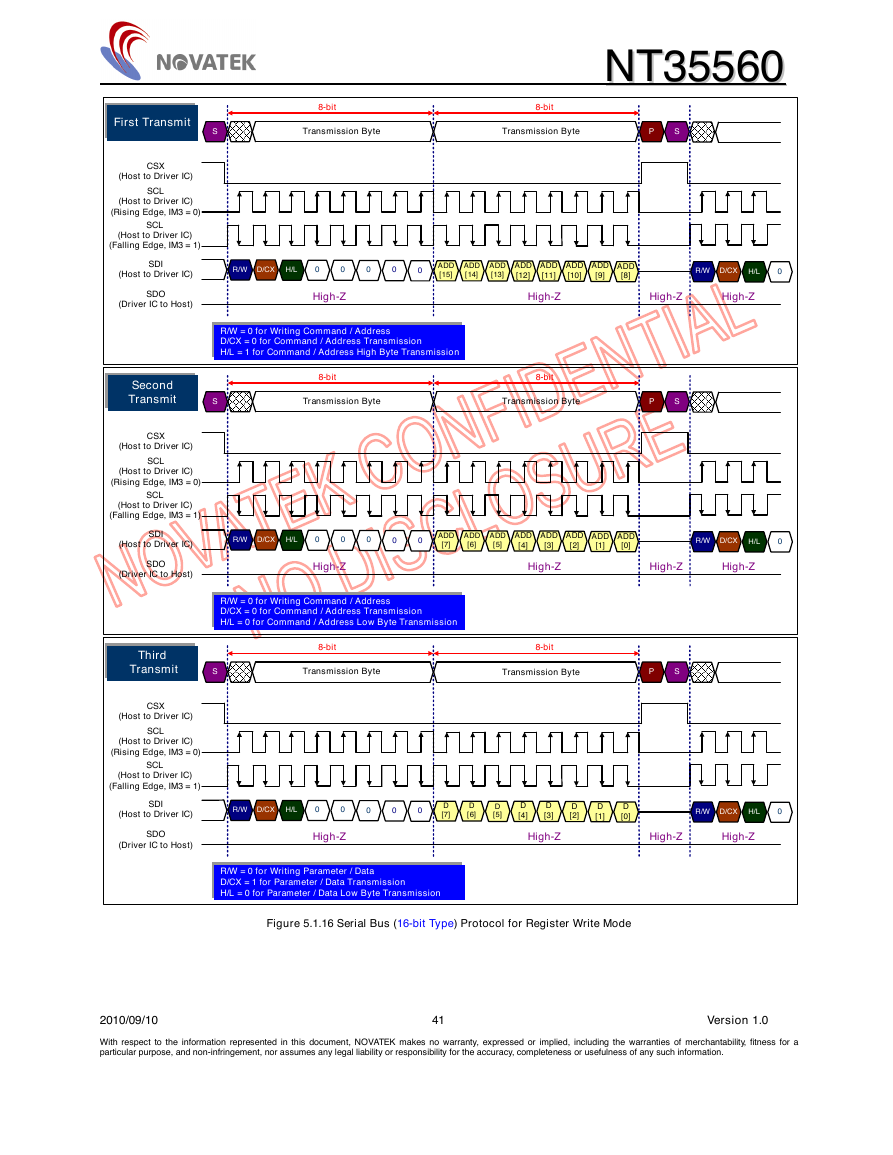
The write mode of the interface means the micro controller writes commands and data to the NT35560. The serial interface is initialized when
CSX is high. In this state, SCL clock pulse or SDI data have no effect. A falling edge on CSX enables the serial interface and indicates the start of
data transmission.
When CSX is high, SCL clock is ignored. During the high time of CSX, the serial interface is initialized. At the falling CSX edge, SCL can be
high or low (See Fig 5.1.16). SDI / SDO is sampled at the rising (or falling) edge of SCL. R/W bit of SPI packet indicates whether the byte is read
command (R/W = '1') or write command (R/W = '0'). It is sampled when first rising (or falling) SCL edge. If CSX stays low after the last bit of
command/data byte, the serial interface expects the R/W bit of the next byte at the next rising (or falling) edge of SCL.
2010/09/10 40 Version 1.0
With respect to the information represented in this document, NOVATEK makes no warranty, expressed or implied, including the warranties of merchantability, fitness for a
particular purpose, and non-infringement, nor assumes any legal liability or responsibility for the accuracy, completeness or usefulness of any such information.
�
NNTT3355556600
8bit
8bit
S
Transmission Byte
Transmission Byte
P
S
First Transmit
CSX
(Host to Driver IC)
SCL
(Host to Driver IC)
(Rising Edge, IM3 = 0)
SCL
(Host to Driver IC)
(Falling Edge, IM3 = 1)
R/W D/CX H/L
0
0
0
0
0
ADD
[15]
ADD
[14]
ADD
[13]
ADD
[12]
ADD
[11]
ADD
[10]
ADD
[9]
ADD
[8]
R/W
D/CX H/L
0
HighZ
HighZ
HighZ
HighZ
R/W = 0 for Writing Command / Address
D/CX = 0 for Command / Address Transmission
H/L = 1 for Command / Address High Byte Transmission
8bit
8bit
S
Transmission Byte
Transmission Byte
P
S
SDI
(Host to Driver IC)
SDO
(Driver IC to Host)
Second
Transmit
CSX
(Host to Driver IC)
SCL
(Host to Driver IC)
(Rising Edge, IM3 = 0)
SCL
(Host to Driver IC)
(Falling Edge, IM3 = 1)
R/W D/CX H/L
0
0
0
0
0
ADD
[7]
ADD
[6]
ADD
[5]
ADD
[4]
ADD
[3]
ADD
[2]
ADD
[1]
ADD
[0]
R/W
D/CX H/L
0
HighZ
HighZ
HighZ
HighZ
R/W = 0 for Writing Command / Address
D/CX = 0 for Command / Address Transmission
H/L = 0 for Command / Address Low Byte Transmission
8bit
8bit
S
Transmission Byte
Transmission Byte
P
S
SDI
(Host to Driver IC)
SDO
(Driver IC to Host)
Third
Transmit
CSX
(Host to Driver IC)
SCL
(Host to Driver IC)
(Rising Edge, IM3 = 0)
SCL
(Host to Driver IC)
(Falling Edge, IM3 = 1)
SDI
(Host to Driver IC)
SDO
(Driver IC to Host)
R/W D/CX H/L
0
0
0
0
0
D
[7]
D
[6]
D
[5]
D
[4]
D
[3]
D
[2]
D
[1]
D
[0]
R/W
D/CX H/L
0
HighZ
HighZ
HighZ
HighZ
R/W = 0 for Writing Parameter / Data
D/CX = 1 for Parameter / Data Transmission
H/L = 0 for Parameter / Data Low Byte Transmission
Figure 5.1.16 Serial Bus (16-bit Type) Protocol for Register Write Mode
2010/09/10 41 Version 1.0
With respect to the information represented in this document, NOVATEK makes no warranty, expressed or implied, including the warranties of merchantability, fitness for a
particular purpose, and non-infringement, nor assumes any legal liability or responsibility for the accuracy, completeness or usefulness of any such information.
�
NNTT3355556600
Figure 5.1.17 Serial Bus (16-bit Type) Protocol for RAM Data Write Mode (An Example with 8-8-8 Pixel Format)
2010/09/10 42 Version 1.0
With respect to the information represented in this document, NOVATEK makes no warranty, expressed or implied, including the warranties of merchantability, fitness for a
particular purpose, and non-infringement, nor assumes any legal liability or responsibility for the accuracy, completeness or usefulness of any such information.
�
NNTT3355556600
5.1.4.2 Read Mode (16-bit Type)
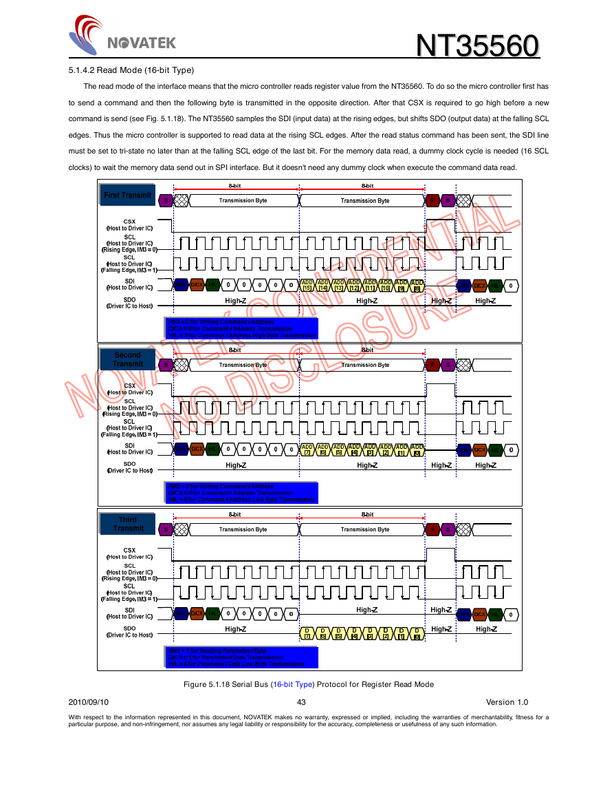
The read mode of the interface means that the micro controller reads register value from the NT35560. To do so the micro controller first has
to send a command and then the following byte is transmitted in the opposite direction. After that CSX is required to go high before a new
command is send (see Fig. 5.1.18). The NT35560 samples the SDI (input data) at the rising edges, but shifts SDO (output data) at the falling SCL
edges. Thus the micro controller is supported to read data at the rising SCL edges. After the read status command has been sent, the SDI line
must be set to tri-state no later than at the falling SCL edge of the last bit. For the memory data read, a dummy clock cycle is needed (16 SCL
clocks) to wait the memory data send out in SPI interface. But it doesn't need any dummy clock when execute the command data read.
Figure 5.1.18 Serial Bus (16-bit Type) Protocol for Register Read Mode
2010/09/10 43 Version 1.0
With respect to the information represented in this document, NOVATEK makes no warranty, expressed or implied, including the warranties of merchantability, fitness for a
particular purpose, and non-infringement, nor assumes any legal liability or responsibility for the accuracy, completeness or usefulness of any such information.
�
NNTT3355556600
5.1.5 Serial Interface (8-bit Type SPI)
The NT35560 provides 8-bit type, 3-wires SPI, it’s also called “LoSSI”. LoSSI supports 8-bit address with 8-bit type parameter(s). When SPI
interface is selected, the “IM4 = 0” is used to setting the 8-bit type, 3-wires SPI. And select IM3 = 0 or 1 to decide the trigger edge of serial clock
(SCL) is rising edge or falling edge. The chip-select CSX (active low) enables and disables the serial interface. RESX (active low) is an external
reset signal. SCL is the serial data clock and SDA is serial data.
Serial data must be input to SDA in the sequence D/CX, D7 to D0. The external host reads the data at the rising / falling edge of SCL signal.
The first bit of serial data D/CX is data/command flag. When D/CX = "1", D7 to D0 bits are display RAM data or command parameters. When
D/CX = "0" D7 to D0 bits are commands.
SCL is not a continuous clock and it can be stopped by the host CPU when SCL is low or high after a rising / falling edge of SCL for D0 in the
writing mode. SCL and SDA can be high or low when there is a falling or rising edge of the CSX.
5.1.5.1 Command Write for LoSSI (8-bit Type SPI)
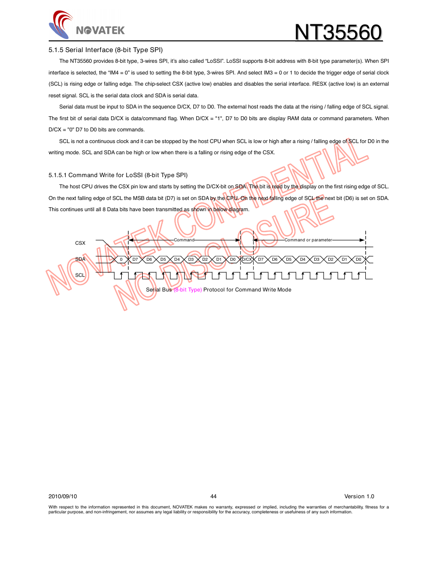
The host CPU drives the CSX pin low and starts by setting the D/CX-bit on SDA. The bit is read by the display on the first rising edge of SCL.
On the next falling edge of SCL the MSB data bit (D7) is set on SDA by the CPU. On the next falling edge of SCL the next bit (D6) is set on SDA.
This continues until all 8 Data bits have been transmitted as shown in below diagram.
CSX
SDA
SCL
Command
Command or parameter
0
D7
D6
D5
D4
D3
D2
D1
D0
D/CX
D7
D6
D5
D4
D3
D2
D1
D0
Serial Bus (8-bit Type) Protocol for Command Write Mode
2010/09/10 44 Version 1.0
With respect to the information represented in this document, NOVATEK makes no warranty, expressed or implied, including the warranties of merchantability, fitness for a
particular purpose, and non-infringement, nor assumes any legal liability or responsibility for the accuracy, completeness or usefulness of any such information.
�
NNTT3355556600
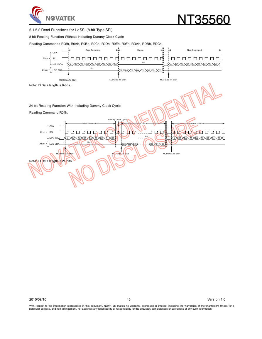
5.1.5.2 Read Functions for LoSSI (8-bit Type SPI)
8-bit Reading Function Without Including Dummy Clock Cycle
Reading Commands R05h, R0Ah, R0Bh, R0Ch, R0Dh, R0Eh, R0Fh, RDAh, RDBh, RDCh.
CSX
SCL
Host
Read Command
ID data
Next Command
MPU SDA
0
D7
D6
D5
D4
D3
D2
D1
D0
Hi-z
0
D7
D6
D5
D4
D3
D2
D1
D0
Driver
LCD SDA
Hi-z
D7
D6
D5
D4
D3
D2
D1
D0
MCU Data Tx Start
LCD Data Tx Start
MCU Data Tx Start
Note: ID Data length is 8-bits.
24-bit Reading Function With Including Dummy Clock Cycle
Reading Command R04h.
Read Command
Dummy Clock Cycle
CSX
SCL
Host
MPU SDA
0
D7
D6
D5
D4
D3
D2
D1
D0
ID data
Hi-z
Next Command
0
D7
D6
D5
D4
D3
D2
D1
D0
Driver
LCD SDA
Hi-z
D23
D22 D21
D2
D1
D0
MCU Data Tx Start
LCD Data Tx Start
MCU Data Tx Start
Note: ID Data length is 24-bits.
2010/09/10 45 Version 1.0
With respect to the information represented in this document, NOVATEK makes no warranty, expressed or implied, including the warranties of merchantability, fitness for a
particular purpose, and non-infringement, nor assumes any legal liability or responsibility for the accuracy, completeness or usefulness of any such information.
�
NNTT3355556600
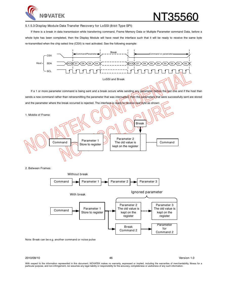
5.1.5.3 Display Module Data Transfer Recovery for LoSSI (8-bit Type SPI)
If there is a break in data transmission while transferring command, Frame Memory Data or Multiple Parameter command Data, before a
whole byte has been completed, then the Display Module will have reset the interface such that it will be ready to receive the same byte
re-transmitted when the chip select line (CSX) is next activated. See the following example:
CSX
Command/Parameter
Break
Command or parameter
Host
SDA
D/CX
D7
D6
D5
D4
D/CX
D7
D6
D5
D4
D3
D2
D1
D0
SCL
LoSSI and Break
If a 1 or more parameter command is being sent and a break occurs while sending any parameter before the last one and if the host then
sends a new command rather than retransmitting the parameter that was interrupted, then the parameters that were successfully sent are stored
and the parameter where the break occurred is rejected. The interface is ready to receive next byte as shown:
1. Middle of Frame:
2. Between Frames:
Break
Command
Parameter 1
Store to register
Parameter 2
The old value is
kept on the register
Command
Without break
Command
Parameter 1
Parameter 2
Parameter 3
With break
Ignored parameter
Command
Parameter 1
Store to register
Parameter 2
The old value is
kept on the
register
Parameter 3
The old value is
kept on the
register
Note: Break can be e.g. another command or noise pulse
Break
Command 2
Parameter
for
Command 2
2010/09/10 46 Version 1.0
With respect to the information represented in this document, NOVATEK makes no warranty, expressed or implied, including the warranties of merchantability, fitness for a
particular purpose, and non-infringement, nor assumes any legal liability or responsibility for the accuracy, completeness or usefulness of any such information.
�
NNTT3355556600
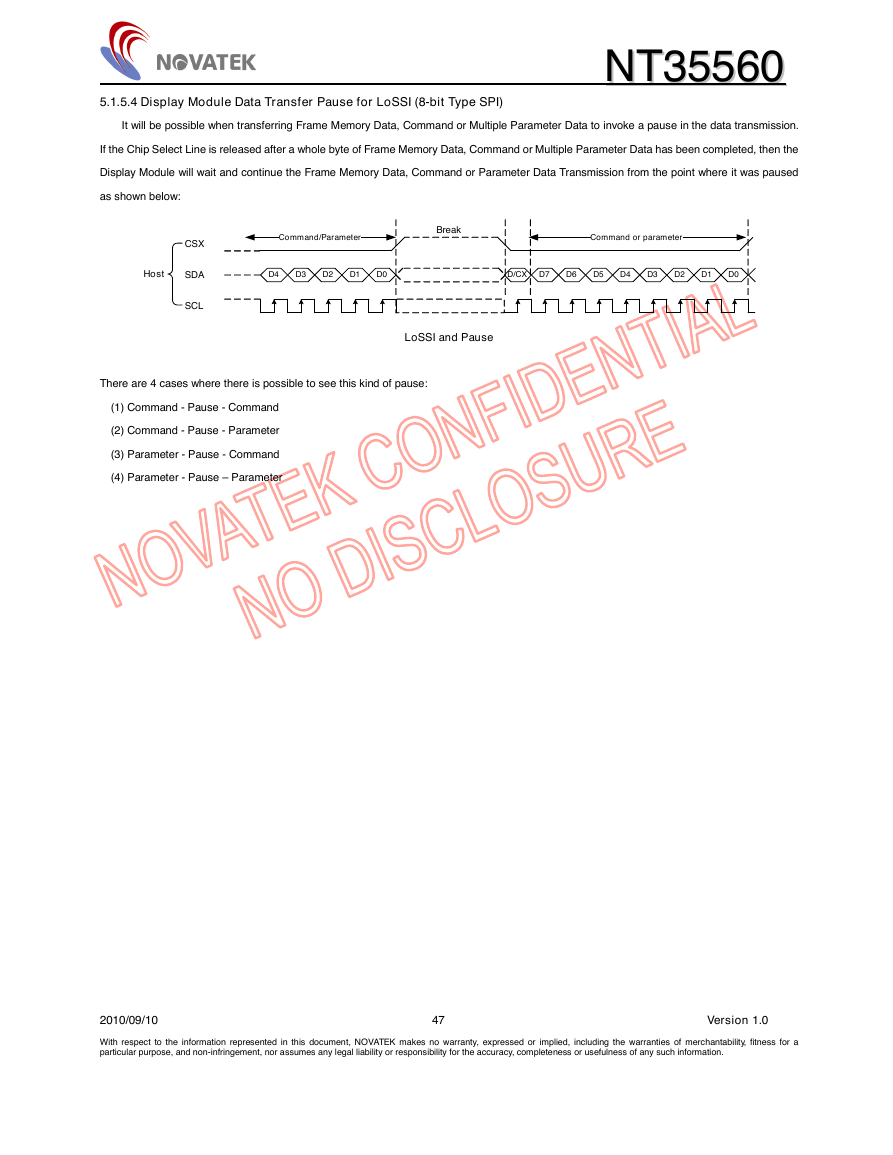
5.1.5.4 Display Module Data Transfer Pause for LoSSI (8-bit Type SPI)
It will be possible when transferring Frame Memory Data, Command or Multiple Parameter Data to invoke a pause in the data transmission.
If the Chip Select Line is released after a whole byte of Frame Memory Data, Command or Multiple Parameter Data has been completed, then the
Display Module will wait and continue the Frame Memory Data, Command or Parameter Data Transmission from the point where it was paused
as shown below:
CSX
Command/Parameter
Break
Command or parameter
Host
SDA
D4
D3
D2
D1
D0
D/CX
D7
D6
D5
D4
D3
D2
D1
D0
SCL
LoSSI and Pause
There are 4 cases where there is possible to see this kind of pause:
(1) Command - Pause - Command
(2) Command - Pause - Parameter
(3) Parameter - Pause - Command
(4) Parameter - Pause – Parameter
2010/09/10 47 Version 1.0
With respect to the information represented in this document, NOVATEK makes no warranty, expressed or implied, including the warranties of merchantability, fitness for a
particular purpose, and non-infringement, nor assumes any legal liability or responsibility for the accuracy, completeness or usefulness of any such information.
�



 2023年江西萍乡中考道德与法治真题及答案.doc
 2012年重庆南川中考生物真题及答案.doc
 2013年江西师范大学地理学综合及文艺理论基础考研真题.doc
 2020年四川甘孜小升初语文真题及答案I卷.doc
 2020年注册岩土工程师专业基础考试真题及答案.doc
 2023-2024学年福建省厦门市九年级上学期数学月考试题及答案.doc
 2021-2022学年辽宁省沈阳市大东区九年级上学期语文期末试题及答案.doc
 2022-2023学年北京东城区初三第一学期物理期末试卷及答案.doc
 2018上半年江西教师资格初中地理学科知识与教学能力真题及答案.doc
 2012年河北国家公务员申论考试真题及答案-省级.doc
 2020-2021学年江苏省扬州市江都区邵樊片九年级上学期数学第一次质量检测试题及答案.doc
 2022下半年黑龙江教师资格证中学综合素质真题及答案.doc