logo资料库

JESD209-3C_Low Power Double Data Rate 3 (LPDDR3).pdf

第1页 / 共158页
第2页 / 共158页
第3页 / 共158页
第4页 / 共158页
第5页 / 共158页
第6页 / 共158页
第7页 / 共158页
第8页 / 共158页
资料共158页,剩余部分请下载后查看
1 Scope
2 Package ballout & Pin Definition
2.1 POP FBGA Ball-outs
2.1.1 216-ball 12 mm x 12 mm, 0.4 mm Pitch Dual-Channel POP FBGA (top view) Using Variation VCCCDB for MO-273
2.1.2 216-ball 12 mm x 12 mm, 0.4 mm Pitch Single Channel A POP FBGA (top view) Using Variation VCCCDB for MO-273
2.1.3 216-ball 12 mm x 12 mm, 0.4 mm Pitch Single Channel B POP FBGA (top view) Using Variation VCCCDB for MO-273
2.1.4 256-ball 14 mm x 14 mm, 0.4 mm Pitch Dual-Channel POP FBGA (top view) Using Variation VEECDB for MO-273
2.1.5 256-ball 14 mm x 14 mm, 0.4 mm Pitch Single Channel-A POP FBGA (top view) Using Variation VEECDB for MO-273
2.1.6 168-ball 12 mm x 12 mm, 0.5 mm pitch single channel x32 PoP with optional e•MMC using Variation VCCBCB for MO-273
2.1.7 272-ball 15 mm x 15 mm, 0.4 mm pitch, Dual-Channel POP FBGA (top view) Using Variation VFFCDB for MO-273
2.1.8 136-ball 10 mm x 10 mm, 0.50 mm pitch POP (e•MMC5.0 + LPDDR3) FBGA (top view), Using Variation xAABCB for MO-273C
2.2 FBGA Package Ball-outs
2.2.1 253-Ball 0.5 mm Pitch Discrete Dual-Channel FBGA (top view) Using Variation EA for MO-276
2.2.2 178-Ball Discrete Single-Channel FBGA (top view) Using Variation AA for MO-311
2.2.3 346-ball 0.5 mm Pitch Dual-Channel Multi-Chip Package (MCP) FBGA (top view) Using Variation AP for MO-276
2.2.4 221-ball 0.5 mm Pitch Multi-Chip Package LPDDR3 x32+eMMC/NAND MCP (top view) Using Variation EB for MO276
2.3 LPDDR3 Pad Sequence
Table 1 — LPDDR3 Pad Sequence
2.4 LPDDDR3 Pad Definition and Description
Table 2 — Pad Definition and Description
3 LPDDR3 Functional Description
3.1 LPDDR3 SDRAM Addressing
Table 3 — LPDDR3 SDRAM Addressing
3.2 Simplified LPDDR3 State Diagram
Figure 1 — LPDDR3: Simplified Bus Interface State Diagram
3.3 Power-up, Initialization, and Power-off
3.3.1 Voltage Ramp and Device Initialization
Table 4 — Voltage Ramp Conditions
Figure 2 — Voltage Ramp and Initialization Sequence
Table 5 — Initialization Timing Parameters
3.3.1.1 Initialization After RESET (without voltage ramp):
3.3.2 Power-off Sequence
Table 6 — Power Supply Conditions
3.3.2.1 Uncontrolled Power-Off Sequence
Table 7 — Timing Parameters Power-Off
3.4 Mode Register Definition
3.4.1 Mode Register Assignment and Definition in LPDDR3 SDRAM
Table 8 — Mode Register Assignment in LPDDR3 SDRAM
MR0 _Device Information (MA<7:0> = 00H):
MR1 _Device Feature 1 (MA<7:0> = 01H):
Table 9 — Burst Sequence
MR2 _Device Feature 2 (MA<7:0> = 02H):
MR3 _I/O Configuration 1 (MA<7:0> = 03H):
MR4 _Device Temperature (MA<7:0> = 04H)
MR5 _Basic Configuration 1 (MA<7:0> = 05H):
MR6 _Basic Configuration 2 (MA<7:0> = 06H):
MR7 _Basic Configuration 3 (MA<7:0> = 07H):
MR8 _Basic Configuration 4 (MA<7:0> = 08BH):
MR9 _Test Mode (MA<7:0> = 09H):
MR10 _Calibration (MA<7:0> = 0AH):
MR11 _ODT Control (MA<7:0> = 0BH:
MR12 :15_(Reserved) (MA<7:0> = 0CH-0FH):
MR16 _PASR_Bank Mask (MA<7:0> = 010H):
MR17 _PASR_Segment Mask (MA<7:0> = 011H):
MR18 -31_Reserved (MA<7:0> = 012H - 01FH):
MR32 _DQ Calibration Pattern A (MA<7:0> = 20H):
MR33 :39_(Do Not Use) (MA<7:0> = 21H-27H):
MR40 _DQ Calibration Pattern B (MA<7:0> = 28H):
MR41 _CA Training_1 (MA<7:0> = 29H):
MR42 _CA Training_2 (MA<7:0> = 2AH):
MR43 :47_(Do Not Use) (MA<7:0> = 2BH-2FH):
MR48 _CA_Training_3 (MA<7:0> = 30H):
MR49 :62_(Reserved) (MA<7:0>=31H-3EH:
MR63 _Reset (MA<7:0> = 3FH): MRW only
MR64 :255_(Reserved) (MA<7:0> = 40H-FFH):
4 LPDDR3 Command Definitions and Timing Diagrams
4.1 Activate Command
Figure 3 — ACTIVATE Command
4.1.1 8-Bank Device Operation
Figure 4 — LPDDR3 tFAW Timing
4.2 LPDDR3 Command Input Signal Timing Definition
Figure 5 — LPDDR3: Command Input Setup and Hold Timing
4.2.1 LPDDR3 CKE Input Setup and Hold Timing
Figure 6 — LPDDR3: Command Input Setup and Hold Timing
4.3 Read and Write access modes
4.4 Burst Read Operation
Figure 7 — Read Output Timing
Figure 8 — Burst Read: RL = 12, BL = 8, tDQSCK > tCK
Figure 9 — Burst Read: RL = 12, BL = 8, tDQSCK < tCK
Figure 10 — LPDDR3: tDQSCKDL timing
Figure 11 — LPDDR3: tDQSCKDM timing
Figure 12 — LPDDR3: tDQSCKDS timing
Figure 13 — Burst Read Followed By Burst Write:
Figure 14 — Seamless Burst Read:
4.5 Burst Write Operation
Figure 15 — Data input (write) timing
Figure 16 — LPDDR3: Burst Write
4.5.1 tWPRECalculation
Figure 17 — Method for Calculating tWPRE Transitions and Endpoints
4.5.2 tWPST Calculation
Figure 18 — Method for Calculating tWPST Transitions and Endpoints
Figure 19 — LPDDR3: Burst Write Followed By Burst Read
Figure 20 — LPDDR3: Seamless burst write: WL = 4, tCCD = 4
4.6 Write Data Mask
Figure 21 — Data Mask Timing
4.7 Precharge Operation
Table 10 — Bank selection for Precharge by address bits
4.7.1 Burst Read operation followed by Precharge
Figure 22 — LPDDR3: Burst Read Followed by Precharge
4.7.2 Burst Write followed by Precharge
Figure 23 — LPDDR3: Burst Write Followed by Precharge
4.7.3 Auto Precharge operation
4.7.3.1 Burst Read with Auto-Precharge
Figure 24 — Burst Read with Auto Precharge
4.7.3.2 Burst write with Auto-Precharge
Figure 25 — Burst Write with Auto Precharge
Table 11 — Precharge & Auto Precharge clarification
4.8 Refresh command
Table 12 — REFRESH Command Scheduling Separation Requirements
Figure 26 — Refresh Command Timing
Figure 27 — Postponing Refresh Commands
Figure 28 — Pulling-in Refresh Commands
4.8.1 Refresh Requirements
Figure 29 — All-Bank REFRESH Operation
Figure 30 — Per-Bank REFRESH Operation
4.9 Self Refresh operation
Figure 31 — LPDDR3: Self-Refresh Operation
4.9.1 Partial Array Self-Refresh (PASR)
4.9.1.1 PASR Bank Masking
4.9.1.2 PASR Segment Masking
Table 13 — Example of Bank and Segment Masking use in LPDDR3 devices
4.10 Mode Register Read (MRR) Command
Figure 32 — Mode Register Read timing example: RL = 8
Figure 33 — xREAD to MRR Timing
Figure 34 — Burst Write Followed by MRR
4.10.0.1 MRR Following Idle Power-Down State
Figure 35 — MRR Following Power-Down Idle State
4.10.1 Temperature Sensor
Table 14 — Temperature Sensor
Figure 36 — Temp Sensor Timing
4.10.2 DQ Calibration
Table 15 — Data Calibration Pattern Description
Figure 37 — DQ Calibration Timing
4.11 Mode Register Write (MRW) Command
Figure 38 — Mode Register Write Timing
4.11.1 Mode Register Write
4.11.1.1 MRW RESET
Table 16 — Truth Table for Mode Register Read (MRR) and Mode Register Write (MRW)
Figure 39 — Mode Register Write Timing for MRW RESET
4.11.2 Mode Register Write ZQ Calibration Command
Figure 40 — ZQ Initialization Timing
Figure 41 — ZQ Calibration Short Timing
Figure 42 — ZQ Calibration Long Timing
Figure 43 — ZQ Calibration Reset Timing
4.11.2.1 ZQ External Resistor Value, Tolerance, and Capacitive Loading
4.11.3 Mode Register Write - CA Training Mode
4.11.3.1 CA Training Sequence
Figure 44 — CA Training Timing Chart
Table 17 — CA Training mode enable ( MR41(29H, 0010 1001B), OP=A4H(1010 0100B) )
Table 18 — CA Training mode disable (MR42(2AH,0010 1010B),OP=A8H(1010 1000B) )
Table 19 — CA to DQ mapping (CA Training mode enabled with MR41)
Table 20 — CA Training mode enable ( MR48(30H, 0011 0000B), OP=C0H(1100 0000B) )
Table 21 — CA to DQ mapping (CA Training mode is enabled with MR48)
4.11.4 Mode Register Write - WR Leveling Mode
Figure 45 — Write Leveling Timing
4.12 On-Die Termination
Figure 46 — Functional Representation of ODT
4.12.1 ODT Mode Register
4.12.2 Asynchronous ODT
4.12.3 ODT During Read Operations (RD or MRR)
4.12.4 ODT During Power Down
4.12.5 ODT During Self Refresh
4.12.6 ODT During Deep Power Down
4.12.7 ODT During CA Training and Write Leveling
Table 22 — DRAM Termination Function In Write Leveling Mode
Table 23 — ODT States Truth Table
Figure 47 — Asynchronous ODT Timing Example for RL = 12
Figure 48 — Automatic ODT Timing During READ Operation Example for RL = m
Figure 49 — ODT Timing During Power Down, Self Refresh, Deep Power Down Entry/Exit Example
4.13 Power-down
Figure 50 — Basic Power-Down Entry and Exit Timing
Figure 51 — CKE-Intensive Environment
Figure 52 — REFRESH-to-REFRESH Timing in CKE-Intensive Environments
Figure 53 — READ to Power-Down Entry
Figure 54 — READ with Auto Precharge to Power-Down Entry
Figure 55 — WRITE to Power-Down Entry
Figure 56 — WRITE with Auto Precharge to Power-Down Entry
Figure 57 — REFRESH Command to Power-Down Entry
Figure 58 — ACTIVATE Command to Power-Down Entry
Figure 59 — PRECHARGE Command to Power-Down Entry
Figure 60 — MRR to Power-Down Entry
Figure 61 — MRW to Power-Down Entry
4.14 Deep Power-Down
Figure 62 — LPDDR3: Deep power down entry and exit timing diagram
4.15 Input clock stop and frequency change
4.16 No Operation command
4.17 Truth tables
4.17.1 Command Truth Table
Table 24 — Command Truth Table
4.17.2 CKE Truth Table
Table 25 — LPDDR3: CKE Table1,2
4.17.3 State Truth Tables
Table 26 — Current State Bank n - Command to Bank n
Table 27 — Current State Bank n - Command to Bank m
4.17.3.1 Data Mask Truth Table
Table 28 — DM truth table
5 Absolute Maximum Ratings
5.1 Absolute Maximum DC Ratings
Table 29 — Absolute Maximum DC Ratings
6 AC & DC Operating Conditions
6.1 Recommended DC Operating Conditions
Table 30 — Recommended DC Operating Conditions
6.2 Input Leakage Current
Table 31 — Input Leakage Current
6.3 Operating Temperature Range
Table 32 — Operating Temperature Range
7 AC and DC Input Measurement Levels
7.1 AC and DC Logic Input Levels for Single-Ended Signals
7.1.1 AC and DC Input Levels for Single-Ended CA and CS_n Signals
Table 33 — Single-Ended AC and DC Input Levels for CA and CS_n Inputs
7.1.2 AC and DC Input Levels for CKE
Table 34 — Single-Ended AC and DC Input Levels for CKE
7.1.3 AC and DC Input Levels for Single-Ended Data Signals
Table 35 — Single-Ended AC and DC Input Levels for DQ and DM
7.2 Vref Tolerances
Figure 63 — Illustration of VRef(DC) tolerance and VRef ac-noise limits
7.3 Input Signal
Figure 64 — LPDDR3 Input Signal
7.4 AC and DC Logic Input Levels for Differential Signals
7.4.1 Differential signal definition
Figure 65 — Definition of differential ac-swing and “time above ac-level” tDVAC
7.4.2 Differential swing requirements for clock (CK_t - CK_c) and strobe (DQS_t - DQS_c)
Table 36 — Differential AC and DC Input Levels
Table 37 — Allowed time before ringback tDVAC for DQS_t/DQS_c
Table 38 — Allowed time before ringback tDVAC for CK_t/CK_c
7.4.3 Single-ended requirements for differential signals
Figure 66 — Single-ended requirement for differential signals.
Table 39 — Single-ended levels for CK_t, DQS_t, CK_c, DQS_c
7.5 Differential Input Cross Point Voltage
Figure 67 — VIX Definition
Table 40 — Cross point voltage for differential input signals (CK, DQS)
7.6 Slew Rate Definitions for Single-Ended Input Signals
7.7 Slew Rate Definitions for Differential Input Signals
Table 41 — Differential Input Slew Rate Definition
Figure 68 — Differential Input Slew Rate Definition for DQS_t, DQS_c and CK_t, CK_c
8 AC and DC Output Measurement Levels
8.1 Single Ended AC and DC Output Levels
Table 42 — Single-ended AC and DC Output Levels
8.2 Differential AC and DC Output Levels
Table 43 — Differential AC and DC Output Levels
8.3 Single Ended Output Slew Rate
Table 44 — Single-ended Output Slew Rate Definition
Figure 69 — Single Ended Output Slew Rate Definition
Table 45 — Output Slew Rate (single-ended)
8.4 Differential Output Slew Rate
Table 46 — Differential Output Slew Rate Definition
Figure 70 — Differential Output Slew Rate Definition
Table 47 — Differential Output Slew Rate
8.5 Overshoot and Undershoot Specifications
Table 48 — AC Overshoot/Undershoot Specification
Figure 71 — Overshoot and Undershoot Definition
8.6 Output buffer characteristics
8.6.1 HSUL_12 Driver Output Timing Reference Load
Figure 72 — HSUL_12 Driver Output Reference Load for Timing and Slew Rate
8.7 RONPU and RONPD Resistor Definition
Figure 73 — Output Driver: Definition of Voltages and Currents
8.7.1 RONPU and RONPD Characteristics with ZQ Calibration
Table 49 — Output Driver DC Electrical Characteristics with ZQ Calibration
8.7.2 Output Driver Temperature and Voltage Sensitivity
Table 50 — Output Driver Sensitivity Definition
Table 51 — Output Driver Temperature and Voltage Sensitivity
8.7.3 RONPU and RONPD Characteristics without ZQ Calibration
Table 52 — Output Driver DC Electrical Characteristics without ZQ Calibration
8.7.4 RZQ I-V Curve
Table 53 — RZQ I-V Curve
Figure 74 — I-V Curve After ZQ Reset
Figure 75 — I-V Curve After Calibration
8.7.5 ODT Levels and I-V Characteristics
Figure 76 — Functional representation of On-Die Termination
Table 54 — ODT DC Electrical Characteristics, assuming RZQ = 240 ohm after proper ZQ calibration
9 Input/Output Capacitance
9.1 Input/Output Capacitance Tables
Table 55 — Input/output capacitance
10 IDD Specification Parameters and Test Conditions
10.1 IDD Measurement Conditions
Table 56 — Definition of Switching for CA Input Signals
Table 57 — Definition of Switching for IDD4R
Table 58 — Definition of Switching for IDD4W
10.2 IDD Specifications
Table 59 — IDD Specification Parameters and Operating Conditions
Table 60 — IDD6 Partial Array Self-Refresh Current
11 Electrical Characteristics and AC Timing
11.1 Clock Specification
11.1.1 Definition for tCK(avg) and nCK
11.1.2 Definition for tCK(abs)
11.1.3 Definition for tCH(avg) and tCL(avg)
11.1.4 Definition for tJIT(per)
11.1.5 Definition for tJIT(cc)
11.1.6 Definition for tERR(nper)
11.1.7 Definition for duty cycle jitter tJIT(duty)
11.1.8 Definition for tCK(abs), tCH(abs) and tCL(abs)
Table 61 — Definition for tCK(abs), tCH(abs), and tCL(abs)
11.2 Period Clock Jitter
11.2.1 Clock period jitter effects on core timing parameters (tRCD, tRP, tRTP, tWR, tWRA, tWTR, tRC, tRAS, tRRD, tFAW )
11.2.1.1 Cycle time de-rating for core timing parameters
11.2.1.2 Clock Cycle de-rating for core timing parameters
11.2.2 Clock jitter effects on Command/Address timing parameters (tISCA, tIHCA, tISCS, tIHCS,tISCKE, tIHCKE, tISb, tIHb, tISCKEb, tIHCKEb)
11.2.3 Clock jitter effects on Read timing parameters
11.2.3.1 tRPRE
11.2.3.2 tLZ(DQ), tHZ(DQ), tDQSCK, tLZ(DQS), tHZ(DQS)
11.2.3.3 tQSH, tQSL
11.2.3.4 tRPST
11.2.4 Clock jitter effects on Write timing parameters
11.2.4.1 tDS, tDH
11.2.4.2 tDSS, tDSH
11.2.4.3 tDQSS
11.3 LPDDR3 Refresh Requirements by Device Density
Table 62 — LPDDR3 Refresh Requirement Parameters (per density)
Table 63 — LPDDR3 Read and Write Latencies
11.4 AC Timing
Table 64 — AC Timing
11.5 CA and CS_n Setup, Hold and Derating
Table 65 — CA Setup and Hold Base-Values
Table 66 — CS_n Setup and Hold Base-Values
Table 67 — Derating values tIS/tIH - ac/dc based AC150
Table 68 — Derating values tIS/tIH - ac/dc based AC135
Table 69 — Required time tVAC above VIH(ac) {below VIL(ac)} for valid transition for CA
Figure 77 — Illustration of nominal slew rate and tVAC for setup time tIS for CA and CS_n with respect to clock.
Figure 78 — Illustration of nominal slew rate for hold time tIH for CA and CS_n with respect to clock
Figure 79 — Illustration of tangent line for setup time tIS for CA and CS_n with respect to clock
Figure 80 — Illustration of tangent line for for hold time tIH for CA and CS_n with respect to clock
11.6 Data Setup, Hold and Slew Rate Derating
Table 70 — Data Setup and Hold Base-Values
Table 71 — Derating values LPDDR3 tDS/tDH - ac/dc based AC150
Table 72 — Derating values LPDDR3 tDS/tDH - ac/dc based AC135
Table 73 — Required time tVAC above VIH(ac) {below VIL(ac)} for valid transition for DQ, DM
Figure 81 — Illustration of nominal slew rate and tVAC for setup time tDS for DQ with respect to strobe
Figure 82 — Illustration of nominal slew rate for hold time tDH for DQ with respect to strobe
Figure 83 — Illustration of tangent line for setup time tDS for DQ with respect to strobe
Figure 84 — Illustration of tangent line for for hold time tDH for DQ with respect to strobe
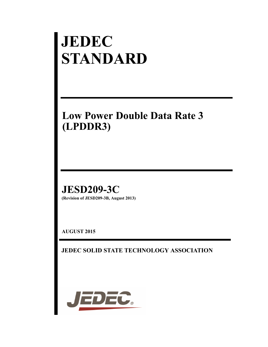
JEDEC STANDARD Low Power Double Data Rate 3 (LPDDR3) JESD209-3C (Revision of JESD209-3B, August 2013) AUGUST 2015 JEDEC SOLID STATE TECHNOLOGY ASSOCIATION
JEDEC standards and publications contain material that has been prepared, reviewed, and approved through the JEDEC Board of Directors level and subsequently reviewed and approved by the JEDEC legal counsel. NOTICE JEDEC standards and publications are designed to serve the public interest through eliminating misunderstandings between manufacturers and purchasers, facilitating interchangeability and improvement of products, and assisting the purchaser in selecting and obtaining with minimum delay the proper product for use by those other than JEDEC members, whether the standard is to be used either domestically or internationally. JEDEC standards and publications are adopted without regard to whether or not their adoption may involve patents or articles, materials, or processes. By such action JEDEC does not assume any liability to any patent owner, nor does it assume any obligation whatever to parties adopting the JEDEC standards or publications. The information included in JEDEC standards and publications represents a sound approach to product specification and application, principally from the solid state device manufacturer viewpoint. Within the JEDEC organization there are procedures whereby a JEDEC standard or publication may be further processed and ultimately become an ANSI standard. No claims to be in conformance with this standard may be made unless all requirements stated in the standard are met. Inquiries, comments, and suggestions relative to the content of this JEDEC standard or publication should be addressed to JEDEC at the address below, or refer to www.jedec.org under Standards and Documents for alternative contact information. Published by ©JEDEC Solid State Technology Association 2015 3103 North 10th Street Suite 240 South Arlington, VA 22201-2107 This document may be downloaded free of charge; however JEDEC retains the copyright on this material. By downloading this file the individual agrees not to charge for or resell the resulting material. PRICE: Contact JEDEC Printed in the U.S.A. All rights reserved
PLEASE! DON'T VIOLATE THE LAW! This document is copyrighted by JEDEC and may not be reproduced without permission. For information, contact: JEDEC Solid State Technology Association 3103 North 10th Street Suite 240 South Arlington, VA 22201-2107 or refer to www.jedec.org under Standards-Documents/Copyright Information.
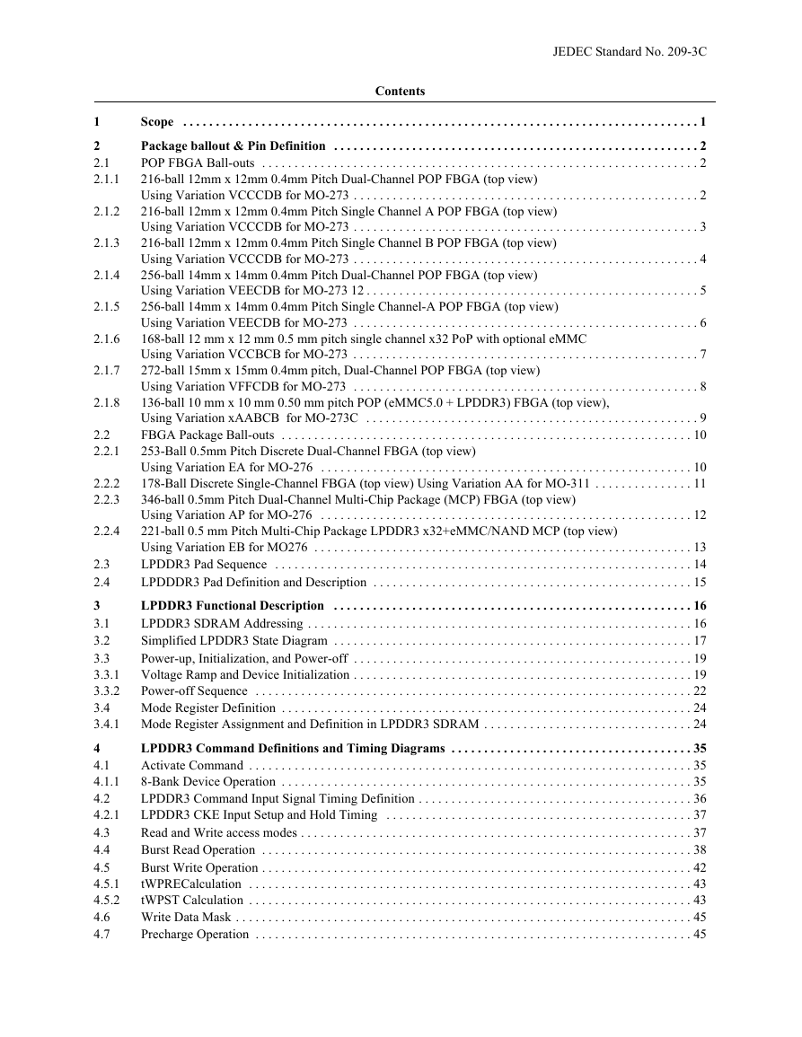
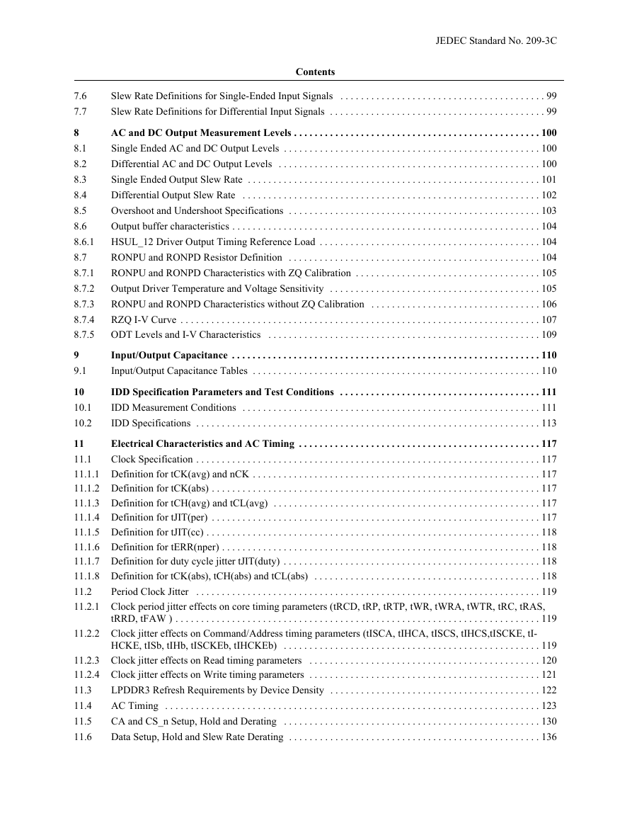
JEDEC Standard No. 209-3C Contents 2.1.2 2.1.3 2.1.4 2.1.5 2.2.4 2.1.8 2.2 2.2.1 2.1.6 2.1.7 2.2.2 2.2.3 1 2 2.1 2.1.1 Scope . . . . . . . . . . . . . . . . . . . . . . . . . . . . . . . . . . . . . . . . . . . . . . . . . . . . . . . . . . . . . . . . . . . . . . . . . . . . . . . 1 Package ballout & Pin Definition . . . . . . . . . . . . . . . . . . . . . . . . . . . . . . . . . . . . . . . . . . . . . . . . . . . . . . . . 2 POP FBGA Ball-outs . . . . . . . . . . . . . . . . . . . . . . . . . . . . . . . . . . . . . . . . . . . . . . . . . . . . . . . . . . . . . . . . . . . 2 216-ball 12mm x 12mm 0.4mm Pitch Dual-Channel POP FBGA (top view) Using Variation VCCCDB for MO-273 . . . . . . . . . . . . . . . . . . . . . . . . . . . . . . . . . . . . . . . . . . . . . . . . . . . . . 2 216-ball 12mm x 12mm 0.4mm Pitch Single Channel A POP FBGA (top view) Using Variation VCCCDB for MO-273 . . . . . . . . . . . . . . . . . . . . . . . . . . . . . . . . . . . . . . . . . . . . . . . . . . . . . 3 216-ball 12mm x 12mm 0.4mm Pitch Single Channel B POP FBGA (top view) Using Variation VCCCDB for MO-273 . . . . . . . . . . . . . . . . . . . . . . . . . . . . . . . . . . . . . . . . . . . . . . . . . . . . . 4 256-ball 14mm x 14mm 0.4mm Pitch Dual-Channel POP FBGA (top view) Using Variation VEECDB for MO-273 12 . . . . . . . . . . . . . . . . . . . . . . . . . . . . . . . . . . . . . . . . . . . . . . . . . . . 5 256-ball 14mm x 14mm 0.4mm Pitch Single Channel-A POP FBGA (top view) Using Variation VEECDB for MO-273 . . . . . . . . . . . . . . . . . . . . . . . . . . . . . . . . . . . . . . . . . . . . . . . . . . . . . 6 168-ball 12 mm x 12 mm 0.5 mm pitch single channel x32 PoP with optional eMMC Using Variation VCCBCB for MO-273 . . . . . . . . . . . . . . . . . . . . . . . . . . . . . . . . . . . . . . . . . . . . . . . . . . . . . 7 272-ball 15mm x 15mm 0.4mm pitch, Dual-Channel POP FBGA (top view) Using Variation VFFCDB for MO-273 . . . . . . . . . . . . . . . . . . . . . . . . . . . . . . . . . . . . . . . . . . . . . . . . . . . . . 8 136-ball 10 mm x 10 mm 0.50 mm pitch POP (eMMC5.0 + LPDDR3) FBGA (top view), Using Variation xAABCB for MO-273C . . . . . . . . . . . . . . . . . . . . . . . . . . . . . . . . . . . . . . . . . . . . . . . . . . . 9 FBGA Package Ball-outs . . . . . . . . . . . . . . . . . . . . . . . . . . . . . . . . . . . . . . . . . . . . . . . . . . . . . . . . . . . . . . . 10 253-Ball 0.5mm Pitch Discrete Dual-Channel FBGA (top view) Using Variation EA for MO-276 . . . . . . . . . . . . . . . . . . . . . . . . . . . . . . . . . . . . . . . . . . . . . . . . . . . . . . . . . 10 178-Ball Discrete Single-Channel FBGA (top view) Using Variation AA for MO-311 . . . . . . . . . . . . . . . 11 346-ball 0.5mm Pitch Dual-Channel Multi-Chip Package (MCP) FBGA (top view) Using Variation AP for MO-276 . . . . . . . . . . . . . . . . . . . . . . . . . . . . . . . . . . . . . . . . . . . . . . . . . . . . . . . . . 12 221-ball 0.5 mm Pitch Multi-Chip Package LPDDR3 x32+eMMC/NAND MCP (top view) Using Variation EB for MO276 . . . . . . . . . . . . . . . . . . . . . . . . . . . . . . . . . . . . . . . . . . . . . . . . . . . . . . . . . . 13 LPDDR3 Pad Sequence . . . . . . . . . . . . . . . . . . . . . . . . . . . . . . . . . . . . . . . . . . . . . . . . . . . . . . . . . . . . . . . . 14 2.3 LPDDDR3 Pad Definition and Description . . . . . . . . . . . . . . . . . . . . . . . . . . . . . . . . . . . . . . . . . . . . . . . . . 15 2.4 LPDDR3 Functional Description . . . . . . . . . . . . . . . . . . . . . . . . . . . . . . . . . . . . . . . . . . . . . . . . . . . . . . . 16 3 LPDDR3 SDRAM Addressing . . . . . . . . . . . . . . . . . . . . . . . . . . . . . . . . . . . . . . . . . . . . . . . . . . . . . . . . . . . 16 3.1 Simplified LPDDR3 State Diagram . . . . . . . . . . . . . . . . . . . . . . . . . . . . . . . . . . . . . . . . . . . . . . . . . . . . . . . 17 3.2 3.3 Power-up, Initialization, and Power-off . . . . . . . . . . . . . . . . . . . . . . . . . . . . . . . . . . . . . . . . . . . . . . . . . . . . 19 3.3.1 Voltage Ramp and Device Initialization . . . . . . . . . . . . . . . . . . . . . . . . . . . . . . . . . . . . . . . . . . . . . . . . . . . . 19 3.3.2 Power-off Sequence . . . . . . . . . . . . . . . . . . . . . . . . . . . . . . . . . . . . . . . . . . . . . . . . . . . . . . . . . . . . . . . . . . . 22 3.4 Mode Register Definition . . . . . . . . . . . . . . . . . . . . . . . . . . . . . . . . . . . . . . . . . . . . . . . . . . . . . . . . . . . . . . . 24 3.4.1 Mode Register Assignment and Definition in LPDDR3 SDRAM . . . . . . . . . . . . . . . . . . . . . . . . . . . . . . . . 24 LPDDR3 Command Definitions and Timing Diagrams . . . . . . . . . . . . . . . . . . . . . . . . . . . . . . . . . . . . . 35 4 4.1 Activate Command . . . . . . . . . . . . . . . . . . . . . . . . . . . . . . . . . . . . . . . . . . . . . . . . . . . . . . . . . . . . . . . . . . . . 35 8-Bank Device Operation . . . . . . . . . . . . . . . . . . . . . . . . . . . . . . . . . . . . . . . . . . . . . . . . . . . . . . . . . . . . . . . 35 4.1.1 LPDDR3 Command Input Signal Timing Definition . . . . . . . . . . . . . . . . . . . . . . . . . . . . . . . . . . . . . . . . . . 36 4.2 LPDDR3 CKE Input Setup and Hold Timing . . . . . . . . . . . . . . . . . . . . . . . . . . . . . . . . . . . . . . . . . . . . . . . 37 4.2.1 4.3 Read and Write access modes . . . . . . . . . . . . . . . . . . . . . . . . . . . . . . . . . . . . . . . . . . . . . . . . . . . . . . . . . . . . 37 Burst Read Operation . . . . . . . . . . . . . . . . . . . . . . . . . . . . . . . . . . . . . . . . . . . . . . . . . . . . . . . . . . . . . . . . . . 38 4.4 Burst Write Operation . . . . . . . . . . . . . . . . . . . . . . . . . . . . . . . . . . . . . . . . . . . . . . . . . . . . . . . . . . . . . . . . . . 42 4.5 4.5.1 tWPRECalculation . . . . . . . . . . . . . . . . . . . . . . . . . . . . . . . . . . . . . . . . . . . . . . . . . . . . . . . . . . . . . . . . . . . . 43 tWPST Calculation . . . . . . . . . . . . . . . . . . . . . . . . . . . . . . . . . . . . . . . . . . . . . . . . . . . . . . . . . . . . . . . . . . . . 43 4.5.2 Write Data Mask . . . . . . . . . . . . . . . . . . . . . . . . . . . . . . . . . . . . . . . . . . . . . . . . . . . . . . . . . . . . . . . . . . . . . . 45 4.6 4.7 Precharge Operation . . . . . . . . . . . . . . . . . . . . . . . . . . . . . . . . . . . . . . . . . . . . . . . . . . . . . . . . . . . . . . . . . . . 45
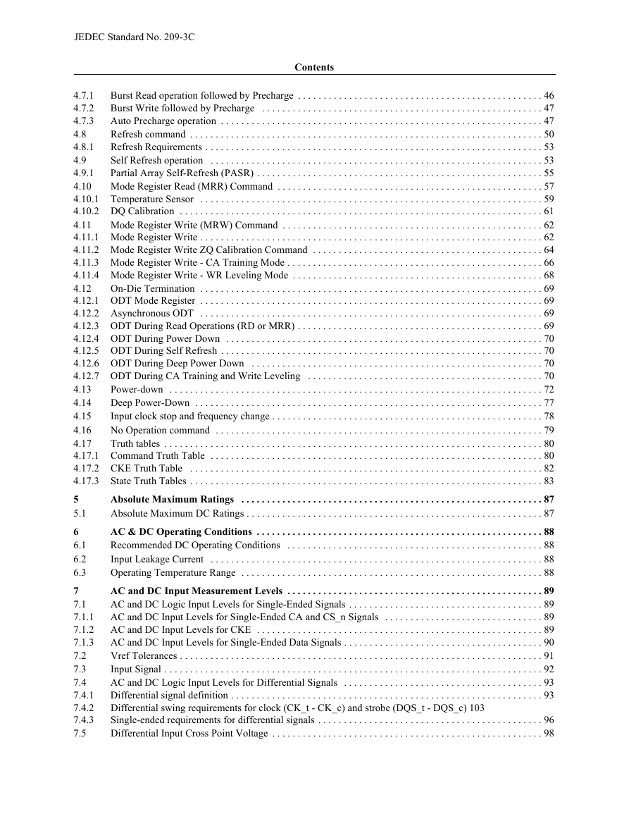
JEDEC Standard No. 209-3C Contents Burst Read operation followed by Precharge . . . . . . . . . . . . . . . . . . . . . . . . . . . . . . . . . . . . . . . . . . . . . . . . 46 4.7.1 4.7.2 Burst Write followed by Precharge . . . . . . . . . . . . . . . . . . . . . . . . . . . . . . . . . . . . . . . . . . . . . . . . . . . . . . . 47 4.7.3 Auto Precharge operation . . . . . . . . . . . . . . . . . . . . . . . . . . . . . . . . . . . . . . . . . . . . . . . . . . . . . . . . . . . . . . . 47 4.8 Refresh command . . . . . . . . . . . . . . . . . . . . . . . . . . . . . . . . . . . . . . . . . . . . . . . . . . . . . . . . . . . . . . . . . . . . . 50 Refresh Requirements . . . . . . . . . . . . . . . . . . . . . . . . . . . . . . . . . . . . . . . . . . . . . . . . . . . . . . . . . . . . . . . . . . 53 4.8.1 Self Refresh operation . . . . . . . . . . . . . . . . . . . . . . . . . . . . . . . . . . . . . . . . . . . . . . . . . . . . . . . . . . . . . . . . . 53 4.9 4.9.1 Partial Array Self-Refresh (PASR) . . . . . . . . . . . . . . . . . . . . . . . . . . . . . . . . . . . . . . . . . . . . . . . . . . . . . . . . 55 4.10 Mode Register Read (MRR) Command . . . . . . . . . . . . . . . . . . . . . . . . . . . . . . . . . . . . . . . . . . . . . . . . . . . . 57 4.10.1 Temperature Sensor . . . . . . . . . . . . . . . . . . . . . . . . . . . . . . . . . . . . . . . . . . . . . . . . . . . . . . . . . . . . . . . . . . . 59 4.10.2 DQ Calibration . . . . . . . . . . . . . . . . . . . . . . . . . . . . . . . . . . . . . . . . . . . . . . . . . . . . . . . . . . . . . . . . . . . . . . . 61 4.11 Mode Register Write (MRW) Command . . . . . . . . . . . . . . . . . . . . . . . . . . . . . . . . . . . . . . . . . . . . . . . . . . . 62 4.11.1 Mode Register Write . . . . . . . . . . . . . . . . . . . . . . . . . . . . . . . . . . . . . . . . . . . . . . . . . . . . . . . . . . . . . . . . . . . 62 4.11.2 Mode Register Write ZQ Calibration Command . . . . . . . . . . . . . . . . . . . . . . . . . . . . . . . . . . . . . . . . . . . . . 64 4.11.3 Mode Register Write - CA Training Mode . . . . . . . . . . . . . . . . . . . . . . . . . . . . . . . . . . . . . . . . . . . . . . . . . . 66 4.11.4 Mode Register Write - WR Leveling Mode . . . . . . . . . . . . . . . . . . . . . . . . . . . . . . . . . . . . . . . . . . . . . . . . . 68 4.12 On-Die Termination . . . . . . . . . . . . . . . . . . . . . . . . . . . . . . . . . . . . . . . . . . . . . . . . . . . . . . . . . . . . . . . . . . . 69 4.12.1 ODT Mode Register . . . . . . . . . . . . . . . . . . . . . . . . . . . . . . . . . . . . . . . . . . . . . . . . . . . . . . . . . . . . . . . . . . . 69 4.12.2 Asynchronous ODT . . . . . . . . . . . . . . . . . . . . . . . . . . . . . . . . . . . . . . . . . . . . . . . . . . . . . . . . . . . . . . . . . . . 69 4.12.3 ODT During Read Operations (RD or MRR) . . . . . . . . . . . . . . . . . . . . . . . . . . . . . . . . . . . . . . . . . . . . . . . . 69 4.12.4 ODT During Power Down . . . . . . . . . . . . . . . . . . . . . . . . . . . . . . . . . . . . . . . . . . . . . . . . . . . . . . . . . . . . . . 70 4.12.5 ODT During Self Refresh . . . . . . . . . . . . . . . . . . . . . . . . . . . . . . . . . . . . . . . . . . . . . . . . . . . . . . . . . . . . . . . 70 4.12.6 ODT During Deep Power Down . . . . . . . . . . . . . . . . . . . . . . . . . . . . . . . . . . . . . . . . . . . . . . . . . . . . . . . . . 70 4.12.7 ODT During CA Training and Write Leveling . . . . . . . . . . . . . . . . . . . . . . . . . . . . . . . . . . . . . . . . . . . . . . 70 4.13 Power-down . . . . . . . . . . . . . . . . . . . . . . . . . . . . . . . . . . . . . . . . . . . . . . . . . . . . . . . . . . . . . . . . . . . . . . . . . 72 Deep Power-Down . . . . . . . . . . . . . . . . . . . . . . . . . . . . . . . . . . . . . . . . . . . . . . . . . . . . . . . . . . . . . . . . . . . . 77 4.14 Input clock stop and frequency change . . . . . . . . . . . . . . . . . . . . . . . . . . . . . . . . . . . . . . . . . . . . . . . . . . . . . 78 4.15 4.16 No Operation command . . . . . . . . . . . . . . . . . . . . . . . . . . . . . . . . . . . . . . . . . . . . . . . . . . . . . . . . . . . . . . . . 79 4.17 Truth tables . . . . . . . . . . . . . . . . . . . . . . . . . . . . . . . . . . . . . . . . . . . . . . . . . . . . . . . . . . . . . . . . . . . . . . . . . . 80 4.17.1 Command Truth Table . . . . . . . . . . . . . . . . . . . . . . . . . . . . . . . . . . . . . . . . . . . . . . . . . . . . . . . . . . . . . . . . . 80 4.17.2 CKE Truth Table . . . . . . . . . . . . . . . . . . . . . . . . . . . . . . . . . . . . . . . . . . . . . . . . . . . . . . . . . . . . . . . . . . . . . 82 4.17.3 State Truth Tables . . . . . . . . . . . . . . . . . . . . . . . . . . . . . . . . . . . . . . . . . . . . . . . . . . . . . . . . . . . . . . . . . . . . . 83 5 Absolute Maximum Ratings . . . . . . . . . . . . . . . . . . . . . . . . . . . . . . . . . . . . . . . . . . . . . . . . . . . . . . . . . . . 87 Absolute Maximum DC Ratings . . . . . . . . . . . . . . . . . . . . . . . . . . . . . . . . . . . . . . . . . . . . . . . . . . . . . . . . . . 87 5.1 AC & DC Operating Conditions . . . . . . . . . . . . . . . . . . . . . . . . . . . . . . . . . . . . . . . . . . . . . . . . . . . . . . . . 88 6 6.1 Recommended DC Operating Conditions . . . . . . . . . . . . . . . . . . . . . . . . . . . . . . . . . . . . . . . . . . . . . . . . . . 88 Input Leakage Current . . . . . . . . . . . . . . . . . . . . . . . . . . . . . . . . . . . . . . . . . . . . . . . . . . . . . . . . . . . . . . . . . 88 6.2 Operating Temperature Range . . . . . . . . . . . . . . . . . . . . . . . . . . . . . . . . . . . . . . . . . . . . . . . . . . . . . . . . . . . 88 6.3 7 AC and DC Input Measurement Levels . . . . . . . . . . . . . . . . . . . . . . . . . . . . . . . . . . . . . . . . . . . . . . . . . . 89 7.1 AC and DC Logic Input Levels for Single-Ended Signals . . . . . . . . . . . . . . . . . . . . . . . . . . . . . . . . . . . . . . 89 7.1.1 AC and DC Input Levels for Single-Ended CA and CS_n Signals . . . . . . . . . . . . . . . . . . . . . . . . . . . . . . . 89 7.1.2 AC and DC Input Levels for CKE . . . . . . . . . . . . . . . . . . . . . . . . . . . . . . . . . . . . . . . . . . . . . . . . . . . . . . . . 89 7.1.3 AC and DC Input Levels for Single-Ended Data Signals . . . . . . . . . . . . . . . . . . . . . . . . . . . . . . . . . . . . . . . 90 Vref Tolerances . . . . . . . . . . . . . . . . . . . . . . . . . . . . . . . . . . . . . . . . . . . . . . . . . . . . . . . . . . . . . . . . . . . . . . . 91 7.2 Input Signal . . . . . . . . . . . . . . . . . . . . . . . . . . . . . . . . . . . . . . . . . . . . . . . . . . . . . . . . . . . . . . . . . . . . . . . . . . 92 7.3 7.4 AC and DC Logic Input Levels for Differential Signals . . . . . . . . . . . . . . . . . . . . . . . . . . . . . . . . . . . . . . . 93 7.4.1 Differential signal definition . . . . . . . . . . . . . . . . . . . . . . . . . . . . . . . . . . . . . . . . . . . . . . . . . . . . . . . . . . . . . 93 7.4.2 Differential swing requirements for clock (CK_t - CK_c) and strobe (DQS_t - DQS_c) 103 7.4.3 7.5 Single-ended requirements for differential signals . . . . . . . . . . . . . . . . . . . . . . . . . . . . . . . . . . . . . . . . . . . . 96 Differential Input Cross Point Voltage . . . . . . . . . . . . . . . . . . . . . . . . . . . . . . . . . . . . . . . . . . . . . . . . . . . . . 98
JEDEC Standard No. 209-3C Contents 7.6 7.7 Slew Rate Definitions for Single-Ended Input Signals . . . . . . . . . . . . . . . . . . . . . . . . . . . . . . . . . . . . . . . . 99 Slew Rate Definitions for Differential Input Signals . . . . . . . . . . . . . . . . . . . . . . . . . . . . . . . . . . . . . . . . . . 99 AC and DC Output Measurement Levels . . . . . . . . . . . . . . . . . . . . . . . . . . . . . . . . . . . . . . . . . . . . . . . . 100 8 Single Ended AC and DC Output Levels . . . . . . . . . . . . . . . . . . . . . . . . . . . . . . . . . . . . . . . . . . . . . . . . . . 100 8.1 Differential AC and DC Output Levels . . . . . . . . . . . . . . . . . . . . . . . . . . . . . . . . . . . . . . . . . . . . . . . . . . . 100 8.2 Single Ended Output Slew Rate . . . . . . . . . . . . . . . . . . . . . . . . . . . . . . . . . . . . . . . . . . . . . . . . . . . . . . . . . 101 8.3 Differential Output Slew Rate . . . . . . . . . . . . . . . . . . . . . . . . . . . . . . . . . . . . . . . . . . . . . . . . . . . . . . . . . . 102 8.4 Overshoot and Undershoot Specifications . . . . . . . . . . . . . . . . . . . . . . . . . . . . . . . . . . . . . . . . . . . . . . . . . 103 8.5 8.6 Output buffer characteristics . . . . . . . . . . . . . . . . . . . . . . . . . . . . . . . . . . . . . . . . . . . . . . . . . . . . . . . . . . . . 104 8.6.1 HSUL_12 Driver Output Timing Reference Load . . . . . . . . . . . . . . . . . . . . . . . . . . . . . . . . . . . . . . . . . . . 104 RONPU and RONPD Resistor Definition . . . . . . . . . . . . . . . . . . . . . . . . . . . . . . . . . . . . . . . . . . . . . . . . . 104 8.7 8.7.1 RONPU and RONPD Characteristics with ZQ Calibration . . . . . . . . . . . . . . . . . . . . . . . . . . . . . . . . . . . . 105 8.7.2 Output Driver Temperature and Voltage Sensitivity . . . . . . . . . . . . . . . . . . . . . . . . . . . . . . . . . . . . . . . . . 105 RONPU and RONPD Characteristics without ZQ Calibration . . . . . . . . . . . . . . . . . . . . . . . . . . . . . . . . . 106 8.7.3 8.7.4 RZQ I-V Curve . . . . . . . . . . . . . . . . . . . . . . . . . . . . . . . . . . . . . . . . . . . . . . . . . . . . . . . . . . . . . . . . . . . . . . 107 8.7.5 ODT Levels and I-V Characteristics . . . . . . . . . . . . . . . . . . . . . . . . . . . . . . . . . . . . . . . . . . . . . . . . . . . . . 109 9 9.1 10 10.1 10.2 Input/Output Capacitance . . . . . . . . . . . . . . . . . . . . . . . . . . . . . . . . . . . . . . . . . . . . . . . . . . . . . . . . . . . . 110 Input/Output Capacitance Tables . . . . . . . . . . . . . . . . . . . . . . . . . . . . . . . . . . . . . . . . . . . . . . . . . . . . . . . . 110 IDD Specification Parameters and Test Conditions . . . . . . . . . . . . . . . . . . . . . . . . . . . . . . . . . . . . . . . 111 IDD Measurement Conditions . . . . . . . . . . . . . . . . . . . . . . . . . . . . . . . . . . . . . . . . . . . . . . . . . . . . . . . . . . 111 IDD Specifications . . . . . . . . . . . . . . . . . . . . . . . . . . . . . . . . . . . . . . . . . . . . . . . . . . . . . . . . . . . . . . . . . . . 113 Electrical Characteristics and AC Timing . . . . . . . . . . . . . . . . . . . . . . . . . . . . . . . . . . . . . . . . . . . . . . . 117 11 11.1 Clock Specification . . . . . . . . . . . . . . . . . . . . . . . . . . . . . . . . . . . . . . . . . . . . . . . . . . . . . . . . . . . . . . . . . . . 117 11.1.1 Definition for tCK(avg) and nCK . . . . . . . . . . . . . . . . . . . . . . . . . . . . . . . . . . . . . . . . . . . . . . . . . . . . . . . . 117 11.1.2 Definition for tCK(abs) . . . . . . . . . . . . . . . . . . . . . . . . . . . . . . . . . . . . . . . . . . . . . . . . . . . . . . . . . . . . . . . . 117 11.1.3 Definition for tCH(avg) and tCL(avg) . . . . . . . . . . . . . . . . . . . . . . . . . . . . . . . . . . . . . . . . . . . . . . . . . . . . 117 11.1.4 Definition for tJIT(per) . . . . . . . . . . . . . . . . . . . . . . . . . . . . . . . . . . . . . . . . . . . . . . . . . . . . . . . . . . . . . . . . 117 11.1.5 Definition for tJIT(cc) . . . . . . . . . . . . . . . . . . . . . . . . . . . . . . . . . . . . . . . . . . . . . . . . . . . . . . . . . . . . . . . . . 118 11.1.6 Definition for tERR(nper) . . . . . . . . . . . . . . . . . . . . . . . . . . . . . . . . . . . . . . . . . . . . . . . . . . . . . . . . . . . . . . 118 11.1.7 Definition for duty cycle jitter tJIT(duty) . . . . . . . . . . . . . . . . . . . . . . . . . . . . . . . . . . . . . . . . . . . . . . . . . . 118 11.1.8 Definition for tCK(abs), tCH(abs) and tCL(abs) . . . . . . . . . . . . . . . . . . . . . . . . . . . . . . . . . . . . . . . . . . . . 118 11.2 Period Clock Jitter . . . . . . . . . . . . . . . . . . . . . . . . . . . . . . . . . . . . . . . . . . . . . . . . . . . . . . . . . . . . . . . . . . . 119 11.2.1 Clock period jitter effects on core timing parameters (tRCD, tRP, tRTP, tWR, tWRA, tWTR, tRC, tRAS, tRRD, tFAW ) . . . . . . . . . . . . . . . . . . . . . . . . . . . . . . . . . . . . . . . . . . . . . . . . . . . . . . . . . . . . . . . . . . . . . . . 119 11.2.2 Clock jitter effects on Command/Address timing parameters (tISCA, tIHCA, tISCS, tIHCS,tISCKE, tI- HCKE, tISb, tIHb, tISCKEb, tIHCKEb) . . . . . . . . . . . . . . . . . . . . . . . . . . . . . . . . . . . . . . . . . . . . . . . . . . 119 11.2.3 Clock jitter effects on Read timing parameters . . . . . . . . . . . . . . . . . . . . . . . . . . . . . . . . . . . . . . . . . . . . . 120 11.2.4 Clock jitter effects on Write timing parameters . . . . . . . . . . . . . . . . . . . . . . . . . . . . . . . . . . . . . . . . . . . . . 121 LPDDR3 Refresh Requirements by Device Density . . . . . . . . . . . . . . . . . . . . . . . . . . . . . . . . . . . . . . . . . 122 11.3 11.4 AC Timing . . . . . . . . . . . . . . . . . . . . . . . . . . . . . . . . . . . . . . . . . . . . . . . . . . . . . . . . . . . . . . . . . . . . . . . . . 123 CA and CS_n Setup, Hold and Derating . . . . . . . . . . . . . . . . . . . . . . . . . . . . . . . . . . . . . . . . . . . . . . . . . . 130 11.5 11.6 Data Setup, Hold and Slew Rate Derating . . . . . . . . . . . . . . . . . . . . . . . . . . . . . . . . . . . . . . . . . . . . . . . . . 136
JEDEC Standard No. 209-3C Contents Annex A Recoginition Page . . . . . . . . . . . . . . . . . . . . . . . . . . . . . . . . . . . . . . . . . . . . . . . . . . . . . . . . . . . . . . . . . . . 142 Annex B Differences between revisions . . . . . . . . . . . . . . . . . . . . . . . . . . . . . . . . . . . . . . . . . . . . . . . . . . . . . . . . . 143
分享到:
收藏