High Speed Serdes Devices and Applications
�
David R. Stauffer • Jeanne Trinko Mechler
Michael Sorna • Kent Dramstad
Clarence R. Ogilvie • Amanullah Mohammad
James Rockrohr
High Speed Serdes Devices
and Applications
�
High Speed Serdes Devices and Applications
Jeanne T. Mechler
IBM Corporation
Essex Junction, VT
USA
Clarence R. Ogilvie
IBM Corporation
Essex Junction, VT
USA
James D. Rockrohr
IBM Microelectronics
Hopewell Junction, NY
USA
iv
David R. Stauffer
IBM Corporation
Essex Junction, VT
USA
Kent Dramstad
IBM Corporation
Essex Junction, VT
USA
Amanullah Mohammad
IBM Corporation
Research Triangle Park, NC
USA
Michael A. Sorna
IBM Microelectronics
Hopewell Junction, NY
USA
ISBN 978-0-387-79833-2
e-ISBN 978-0-387-79834-9
Library of Congress Control Number: 2008925643
© 2008 Springer Science+Business Media, LLC
All rights reserved. This work may not be translated or copied in whole or in part without the written per-
mission of the publisher (Springer Science+Business Media, LLC, 233 Spring Street, New York, NY 10013,
USA), except for brief excerpts in connection with reviews or scholarly analysis. Use in connection with any
form of information storage and retrieval, electronic adaptation, computer software, or by similar or dissimilar
methodology now known or heareafter developed is forbidden. The use in this publication of trade names,
trademarks, service marks, and similar terms, even if they are not identified as such, is not to be taken as an
expression of opinion as to whether or not they are subject to proprietary rights.
While the advice and information in this book are believed to be true and accurate at the date of going to
press, neither the authors nor the editors nor the publisher can accept any legal responsibility for any errors
or omissions that may be made. The publisher makes no warranty, express or implied, with respect to the
material contained herein.
Printed on acid-free paper.
9 8 7 6 5 4 3 2 1
springer.com
�
v
Preface
The simplest method of transferring data through the inputs or outputs of a
silicon chip is to directly connect each bit of the datapath from one chip to the
next chip. Once upon a time this was an acceptable approach. However, one
aspect (and perhaps the only aspect) of chip design which has not changed
during the career of the authors is Moore’s Law, which has dictated substantial
increases in the number of circuits that can be manufactured on a chip. The pin
densities of chip packaging technologies have not increased at the same pace
as has silicon density, and this has led to a prevalence of High Speed Serdes
(HSS) devices as an inherent part of almost any chip design.
HSS devices are the dominant form of input/output for many (if not most)
high-integration chips, moving serial data between chips at speeds up to 10
Gbps and beyond. Chip designers with a background in digital logic design
tend to view HSS devices as simply complex digital input/output cells. This
view ignores the complexity associated with serially moving billions of bits of
data per second. At these data rates, the assumptions associated with digital
signals break down and analog factors demand consideration. The chip
designer who oversimplifies the problem does so at his or her own peril.
Despite this, many chip designers who undertake using HSS cores in their
design do not have a sufficient background to make informed decisions on the
use of HSS features in their application, and to appreciate the potential pitfalls
that result from ignoring the analog nature of the application. Databooks
describe the detailed features of specific HSS devices, but usually assume that
the reader already understands the fundamentals. This is the equivalent of
providing detailed descriptions of the trees, but leaving the reader struggling to
get an overview of the forest.
This text is intended to bridge this gap, and provide the reader with a broad
understanding of HSS device usage. Topics typically taught in a variety of
courses using multiple texts are consolidated in this text to provide sufficient
background for the chip designer that is using HSS devices on his or her chip.
This text may be viewed as consisting of four sections as outlined below.
The first three chapters relate to the features, functions, and design of HSS
devices. Chapter 1 introduces the reader to the basic concepts and the resulting
features and functions typical of HSS devices. Chapter 2 builds upon these
concepts by describing an example of an HSS core, thereby giving the reader
a concrete implementation to use as a framework for topics throughout the
remainder of the text. Although loosely based on the HSS designs offered in
IBM ASIC products, this HSS EX10 is a simplified tutorial example and shares
many features/functions with product offerings from other vendors. Finally,
Chap. 3 introduces interested readers to the architecture and design of HSS
cores using the HSS EX10 as an example.
The next two chapters describe the features and functions of protocol logic
used to implement various network protocol interface standards. Chapter 4
v
�
vi
introduces concepts related to interface standards, as well as design
architectures for various protocol logic functions. Chapter 5 provides an
overview of various protocol standards in which HSS cores are used.
High Speed Serdes Devices and Applications
The next four chapters cover specialized topics related to HSS cores.
Chapter 6 describes clock architectures for the reference clock network which
supplies clocks to the HSS core, as well as floorplanning and signal integrity
analysis of these networks. Chapter 7 covers various topics related to testing
HSS cores and diagnostics using HSS cores. Chapter 8 covers basic concepts
regarding signal integrity, and signal integrity analysis methods. Chapter 9
covers power dissipation concepts and how these relate to HSS cores.
Finally, any HSS core is not complete without a set of design kit models to
facilitate integration within the chip design. Chapter 10 discusses various
topics regarding the design kit models that require special consideration when
applied to HSS cores.
�
vii
Acknowledgments
The authors wish to thank the following IBM colleagues without whose
contributions and reviews this text would not be possible: William Clark,
Nanju Na, Stephen Kessler, Ed Pillai, M. Chandrika, Peter Jenkins, Douglas
Massey, Suzanne Granato, Della Budell, and Jack Smith.
In addition, the authors would like to thank Thucydides Xanthopoulos of
Cavium Networks for his detailed and insightful review of this text, and
Andrea Kosich for making it possible to utilize material from Optical
Internetworking Forum Interoperability Agreements.
vii
�
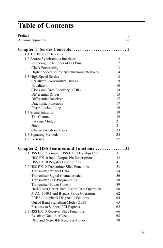
Table of Contents
Table of Contents
Preface
Acknowledgments
ix
v
vii
Chapter 1: Serdes Concepts. . . . . . . . . . . . . . . . . . . . . . . . . 1
1.1 The Parallel Data Bus
1.2 Source Synchronous Interfaces
Reducing the Number of I/O Pins
Clock Forwarding
Higher Speed Source Synchronous Interfaces
1.3 High-Speed Serdes
Serializer / Deserializer Blocks
Equalizers
Clock and Data Recovery (CDR)
Differential Driver
Differential Receiver
Diagnostic Functions
Phase-Locked Loop
1.4 Signal Integrity
The Channel
Package Models
Jitter
Channel Analysis Tools
1.5 Signaling Methods
1.6 Exercises
1
2
2
3
4
8
9
10
14
15
17
17
19
19
19
21
21
23
24
27
31
32
41
53
54
56
58
59
60
62
64
65
65
66
68
70
Chapter 2: HSS Features and Functions . . . . . . . . . . . . . 31
2.1 HSS Core Example: HSS EX10 10-Gbps Core
HSS EX10 Input/Output Pin Descriptions
HSS EX10 Register Descriptions
2.2 HSS EX10 Transmitter Slice Functions
Transmitter Parallel Data
Transmitter Signal Characteristics
Transmitter FFE Programming
Transmitter Power Control
Half-Rate/Quarter-Rate/Eighth-Rate Operation
JTAG 1149.1 and Bypass Mode Operation
PRBS / Loopback Diagnostic Features
Out of Band Signalling Mode (OBS)
Features to Support PCI Express
2.3 HSS EX10 Receiver Slice Functions
Receiver Data Interface
DFE and Non-DFE Receiver Modes
ix
�
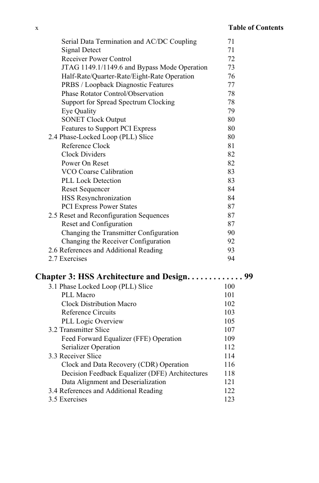
x
Serial Data Termination and AC/DC Coupling
Signal Detect
Receiver Power Control
JTAG 1149.1/1149.6 and Bypass Mode Operation
Half-Rate/Quarter-Rate/Eight-Rate Operation
PRBS / Loopback Diagnostic Features
Phase Rotator Control/Observation
Support for Spread Spectrum Clocking
Eye Quality
SONET Clock Output
Features to Support PCI Express
2.4 Phase-Locked Loop (PLL) Slice
Reference Clock
Clock Dividers
Power On Reset
VCO Coarse Calibration
PLL Lock Detection
Reset Sequencer
HSS Resynchronization
PCI Express Power States
2.5 Reset and Reconfiguration Sequences
Reset and Configuration
Changing the Transmitter Configuration
Changing the Receiver Configuration
2.6 References and Additional Reading
2.7 Exercises
Table of Contents
71
71
72
73
76
77
78
78
79
80
80
80
81
82
82
83
83
84
84
87
87
87
90
92
93
94
Chapter 3: HSS Architecture and Design. . . . . . . . . . . . . 99
3.1 Phase Locked Loop (PLL) Slice
PLL Macro
Clock Distribution Macro
Reference Circuits
PLL Logic Overview
3.2 Transmitter Slice
Feed Forward Equalizer (FFE) Operation
Serializer Operation
3.3 Receiver Slice
Clock and Data Recovery (CDR) Operation
Decision Feedback Equalizer (DFE) Architectures
Data Alignment and Deserialization
3.4 References and Additional Reading
3.5 Exercises
100
101
102
103
105
107
109
112
114
116
118
121
122
123
�




 2023年江西萍乡中考道德与法治真题及答案.doc
 2012年重庆南川中考生物真题及答案.doc
 2013年江西师范大学地理学综合及文艺理论基础考研真题.doc
 2020年四川甘孜小升初语文真题及答案I卷.doc
 2020年注册岩土工程师专业基础考试真题及答案.doc
 2023-2024学年福建省厦门市九年级上学期数学月考试题及答案.doc
 2021-2022学年辽宁省沈阳市大东区九年级上学期语文期末试题及答案.doc
 2022-2023学年北京东城区初三第一学期物理期末试卷及答案.doc
 2018上半年江西教师资格初中地理学科知识与教学能力真题及答案.doc
 2012年河北国家公务员申论考试真题及答案-省级.doc
 2020-2021学年江苏省扬州市江都区邵樊片九年级上学期数学第一次质量检测试题及答案.doc
 2022下半年黑龙江教师资格证中学综合素质真题及答案.doc