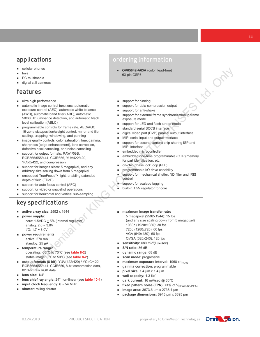
applications
features
key specifications
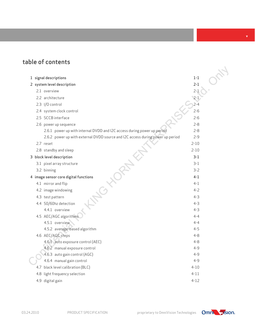
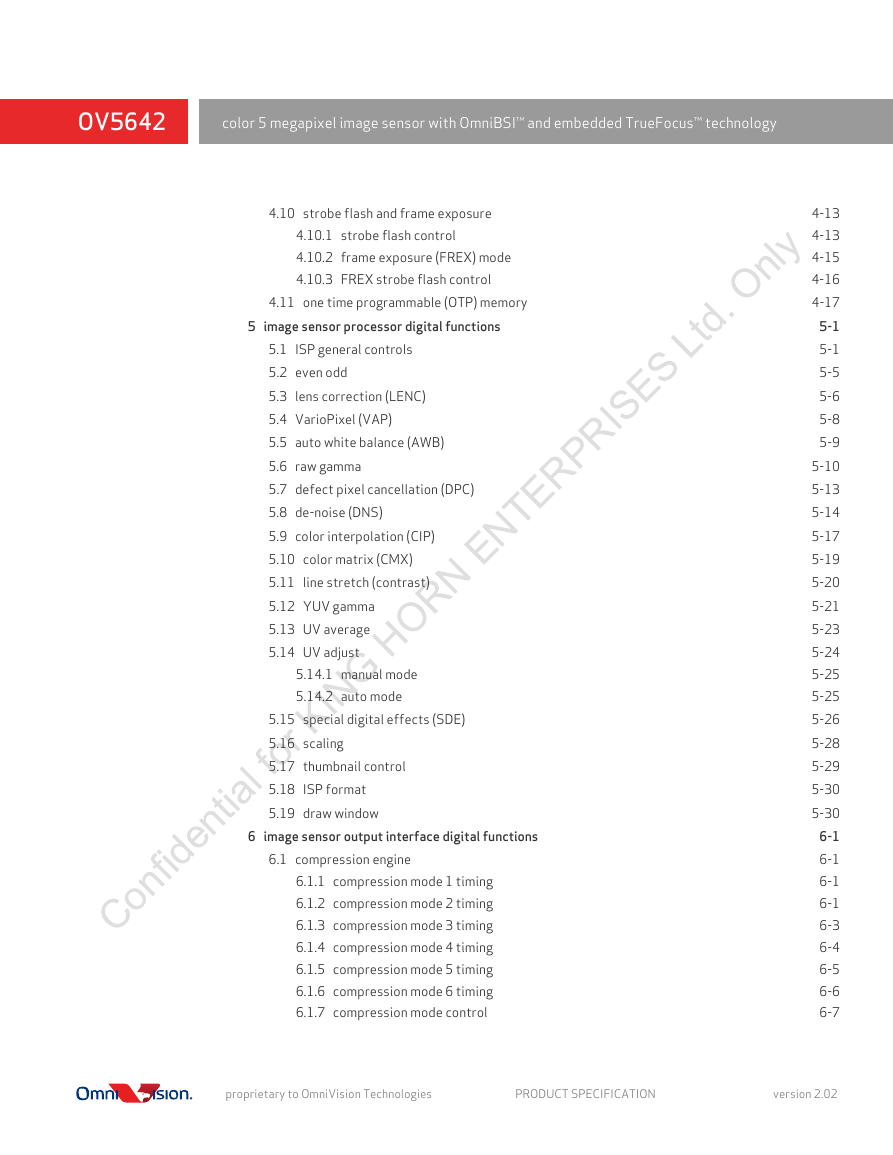
table of contents
list of figures
list of tables
1 signal descriptions
table 1-1 signal descriptions (sheet 1 of 3)
figure 1-1 pin diagram
2 system level description
2.1 overview
2.2 architecture
figure 2-1 OV5642 block diagram
figure 2-2 reference design schematic
2.3 I/O control
table 2-1 driving capability and direction control for I/O pads (sheet 1 of 2)
2.4 system clock control
2.5 SCCB interface
table 2-2 group sharing registers
table 2-3 group write register
2.6 power up sequence
2.6.1 power up with internal DVDD and I2C access during power up period
figure 2-3 power up timing with internal DVDD and I2C access during power up period
2.6.2 power up with external DVDD source and I2C access during power up period
figure 2-4 power up timing with external DVDD source and I2C access during power up period
2.7 reset
2.8 standby and sleep
3 block level description
3.1 pixel array structure
figure 3-1 sensor array region color filter layout
3.2 binning
figure 3-2 example of 2x2 binning
table 3-1 binning-related registers
4 image sensor core digital functions
4.1 mirror and flip
figure 4-1 mirror and flip samples
table 4-1 mirror and flip registers
4.2 image windowing
figure 4-2 image windowing
table 4-2 image windowing registers
4.3 test pattern
figure 4-3 test pattern
table 4-3 test pattern selection control
4.4 50/60hz detection
4.4.1 overview
4.5 AEC/AGC algorithms
4.5.1 overview
table 4-4 AEC/AGC control functions
4.5.2 average-based algorithm
figure 4-4 desired convergence
table 4-5 AEC/AGC control functions
figure 4-5 average-based window definition
table 4-6 average-based algorithm functions
4.6 AEC/AGC steps
4.6.1 auto exposure control (AEC)
4.6.2 manual exposure control
4.6.3 auto gain control (AGC)
4.6.4 manual gain control
4.7 black level calibration (BLC)
table 4-7 BLC control functions (sheet 1 of 2)
4.8 light frequency selection
table 4-8 light frequency registers
4.9 digital gain
table 4-9 digital gain control functions
4.10 strobe flash and frame exposure
4.10.1 strobe flash control
table 4-10 flashlight modes
figure 4-6 xenon flash mode
figure 4-7 LED 1 & 2 mode - one pulse output
figure 4-8 LED 1 & 2 mode - multiple pulse output
figure 4-9 LED 3 mode
4.10.2 frame exposure (FREX) mode
figure 4-10 FREX modes
4.10.3 FREX strobe flash control
table 4-11 FREX strobe control functions
4.11 one time programmable (OTP) memory
table 4-12 OTP control functions
5 image sensor processor digital functions
5.1 ISP general controls
table 5-1 ISP general control registers (sheet 1 of 4)
5.2 even odd
table 5-2 even odd control registers
5.3 lens correction (LENC)
table 5-3 LENC control registers (sheet 1 of 2)
5.4 VarioPixel (VAP)
table 5-4 VAP control registers
5.5 auto white balance (AWB)
table 5-5 AWB control registers
5.6 raw gamma
table 5-6 raw gamma control registers (sheet 1 of 3)
5.7 defect pixel cancellation (DPC)
table 5-7 DPC control registers
5.8 de-noise (DNS)
table 5-8 DNS control registers (sheet 1 of 3)
5.9 color interpolation (CIP)
table 5-9 CIP control registers (sheet 1 of 2)
5.10 color matrix (CMX)
table 5-10 CMX control registers (sheet 1 of 2)
5.11 line stretch (contrast)
table 5-11 line stretch (contrast) control registers (sheet 1 of 2)
5.12 YUV gamma
table 5-12 YUV gamma control registers (sheet 1 of 3)
5.13 UV average
table 5-13 UV average register
5.14 UV adjust
table 5-14 UV adjust control registers
5.14.1 manual mode
5.14.2 auto mode
figure 5-1 UV adjust graph
5.15 special digital effects (SDE)
table 5-15 SDE control registers (sheet 1 of 2)
5.16 scaling
table 5-16 scaling control registers
5.17 thumbnail control
table 5-17 DCW control registers
5.18 ISP format
table 5-18 ISP format control registers
5.19 draw window
table 5-19 draw window registers (sheet 1 of 2)
6 image sensor output interface digital functions
6.1 compression engine
6.1.1 compression mode 1 timing
figure 6-1 compression mode 1 timing
6.1.2 compression mode 2 timing
figure 6-2 compression mode 2 timing
figure 6-3 compression mode 2 (with thumbnail data) timing
figure 6-4 image footer
6.1.3 compression mode 3 timing
figure 6-5 compression mode 3 timing
6.1.4 compression mode 4 timing
figure 6-6 compression mode 4 timing
6.1.5 compression mode 5 timing
figure 6-7 compression mode 5 timing
6.1.6 compression mode 6 timing
figure 6-8 compression mode 6 timing
6.1.7 compression mode control
table 6-1 compression control registers (sheet 1 of 2)
6.2 system control
table 6-2 system control registers (sheet 1 of 3)
6.3 microcontroller unit (MCU)
table 6-3 MCU control registers (sheet 1 of 2)
6.4 camera interface (CIF)
table 6-4 CIF control registers
6.5 frame control (FC)
table 6-5 FC control registers
6.6 format description
table 6-6 FORMAT control registers (sheet 1 of 5)
6.7 digital video port (DVP)
6.7.1 overview
table 6-7 DVP control registers (sheet 1 of 2)
6.7.2 DVP timing
figure 6-9 DVP timing diagram
table 6-8 DVP timing specifications (sheet 1 of 2)
6.8 mobile industry processor interface (MIPI)
table 6-9 MIPI receiver registers
table 6-10 MIPI transmitter registers (sheet 1 of 5)
7 register tables
table 7-1 system and IO pad control registers (sheet 1 of 7)
table 7-2 SCCB control registers
table 7-3 group write control registers
table 7-4 AWB (for power keep domain in AWB gain) registers
table 7-5 AEC/AGC (for power keep domain in AEC/AGC) registers
table 7-6 sensor control registers
table 7-7 timing control registers (sheet 1 of 3)
table 7-8 power down domain AEC/AGC registers (sheet 1 of 4)
table 7-9 FREX strobe registers
table 7-10 light frequency registers
table 7-11 OTP registers
table 7-12 MCU registers (sheet 1 of 2)
table 7-13 BLC registers (sheet 1 of 2)
table 7-14 CIF registers
table 7-15 frame control registers
table 7-16 format registers (sheet 1 of 5)
table 7-17 compression registers (sheet 1 of 2)
table 7-18 IFIFO control registers
table 7-19 VFIFO registers
table 7-20 DVP registers (sheet 1 of 2)
table 7-21 MIPI transmitter (TX) registers (sheet 1 of 6)
table 7-22 ISP frame control registers
table 7-23 MIPI receiver (RX) registers
table 7-24 ISP top control registers (sheet 1 of 6)
table 7-25 AWB registers (sheet 1 of 3)
table 7-26 de-noise (DNS) registers (sheet 1 of 3)
table 7-27 CIP registers (sheet 1 of 2)
table 7-28 CMX registers (sheet 1 of 2)
table 7-29 stretch registers (sheet 1 of 2)
table 7-30 raw gamma / Y gamma registers
table 7-31 UV gamma registers (sheet 1 of 2)
table 7-32 UV adjust registers
table 7-33 SDE registers
table 7-34 scale/average registers (sheet 1 of 2)
table 7-35 DCW and DPC registers (sheet 1 of 3)
table 7-36 LENC registers (sheet 1 of 7)
table 7-37 AFC control registers (sheet 1 of 5)
8 operating specifications
8.1 absolute maximum ratings
table 8-1 absolute maximum ratings
8.2 functional temperature
table 8-2 functional temperature
8.3 DC characteristics
table 8-3 DC characteristics (-20°C < TA < 70°C) (sheet 1 of 2)
8.4 AC characteristics
table 8-4 AC characteristics (TA = 25°C, VDD-A = 2.8V)
table 8-5 timing characteristics
figure 8-1 SCCB interface timing
table 8-6 SCCB interface timing specifications
figure 8-2 line/pixel output timing
table 8-7 pixel timing specifications
9 mechanical specifications
9.1 physical specifications
figure 9-1 package specifications
table 9-1 package dimensions
9.2 IR reflow specifications
figure 9-2 IR reflow ramp rate requirements
table 9-2 reflow conditions
10 optical specifications
10.1 sensor array center
figure 10-1 sensor array center
10.2 lens chief ray angle (CRA)
figure 10-2 chief ray angle (CRA)
table 10-1 CRA versus image height plot (sheet 1 of 2)
revision history



 2023年江西萍乡中考道德与法治真题及答案.doc
 2012年重庆南川中考生物真题及答案.doc
 2013年江西师范大学地理学综合及文艺理论基础考研真题.doc
 2020年四川甘孜小升初语文真题及答案I卷.doc
 2020年注册岩土工程师专业基础考试真题及答案.doc
 2023-2024学年福建省厦门市九年级上学期数学月考试题及答案.doc
 2021-2022学年辽宁省沈阳市大东区九年级上学期语文期末试题及答案.doc
 2022-2023学年北京东城区初三第一学期物理期末试卷及答案.doc
 2018上半年江西教师资格初中地理学科知识与教学能力真题及答案.doc
 2012年河北国家公务员申论考试真题及答案-省级.doc
 2020-2021学年江苏省扬州市江都区邵樊片九年级上学期数学第一次质量检测试题及答案.doc
 2022下半年黑龙江教师资格证中学综合素质真题及答案.doc