32418_fm.pdf
Front Matter
About the Author
Preface
Table of Contents
Index
A
B
C
D
E
F
G
H
I
J
K
L
M
N
O
P
Q
R
S
T
U
V
W
X
Y
Z
32418_toc.pdf
Front Matter
Preface
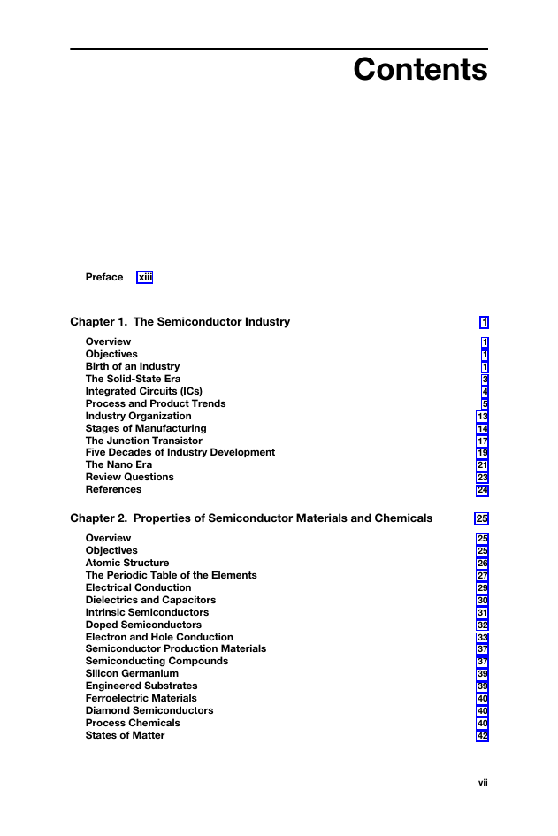
Table of Contents
1. The Semiconductor Industry
1.1 Overview
1.2 Objectives
1.3 Birth of an Industry
1.4 The Solid-State Era
1.5 Integrated Circuits (ICs)
1.6 Process and Product Trends
1.7 Industry Organization
1.8 Stages of Manufacturing
1.9 The Junction Transistor
1.10 Five Decades of Industry Development
1.11 The Nano Era
1.12 Review Questions
1.13 References
2. Properties of Semiconductor Materials and Chemicals
2.1 Overview
2.2 Objectives
2.3 Atomic Structure
2.4 The Periodic Table of the Elements
2.5 Electrical Conduction
2.6 Dielectrics and Capacitors
2.7 Intrinsic Semiconductors
2.8 Doped Semiconductors
2.9 Electron and Hole Conduction
2.10 Semiconductor Production Materials
2.11 Semiconducting Compounds
2.12 Silicon Germanium
2.13 Engineered Substrates
2.14 Ferroelectric Materials
2.15 Diamond Semiconductors
2.16 Process Chemicals
2.17 States of Matter
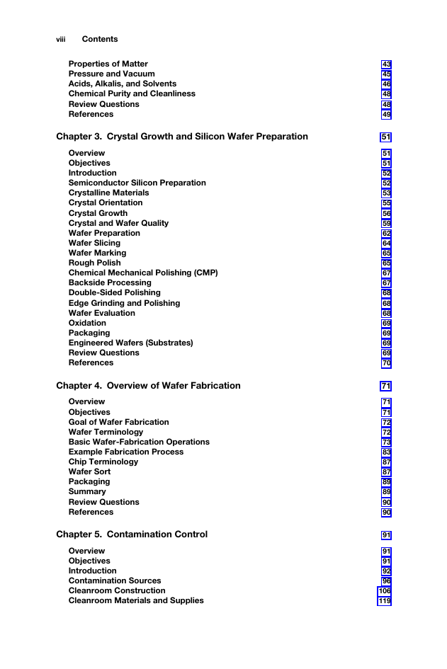
2.18 Properties of Matter
2.19 Pressure and Vacuum
2.20 Acids, Alkalis, and Solvents
2.21 Chemical Purity and Cleanliness
2.22 Review Questions
2.23 References
3. Crystal Growth and Silicon Wafer Preparation
3.1 Overview
3.2 Objectives
3.3 Introduction
3.4 Semiconductor Silicon Preparation
3.5 Crystalline Materials
3.6 Crystal Orientation
3.7 Crystal Growth
3.8 Crystal and Wafer Quality
3.9 Wafer Preparation
3.10 Wafer Slicing
3.11 Wafer Marking
3.12 Rough Polish
3.13 Chemical Mechanical Polishing (CMP)
3.14 Backside Processing
3.15 Double-Sided Polishing
3.16 Edge Grinding and Polishing
3.17 Wafer Evaluation
3.18 Oxidation
3.19 Packaging
3.20 Engineered Wafers (Substrates)
3.21 Review Questions
3.22 References
4. Overview of Wafer Fabrication
4.1 Overview
4.2 Objectives
4.3 Goal of Wafer Fabrication
4.4 Wafer Terminology
4.5 Basic Wafer-Fabrication Operations
4.6 Example Fabrication Process
4.7 Chip Terminology
4.8 Wafer Sort
4.9 Packaging
4.10 Summary
4.11 Review Questions
4.12 References
5. Contamination Control
5.1 Overview
5.2 Objectives
5.3 Introduction
5.4 Contamination Sources
5.5 Cleanroom Construction
5.6 Cleanroom Materials and Supplies
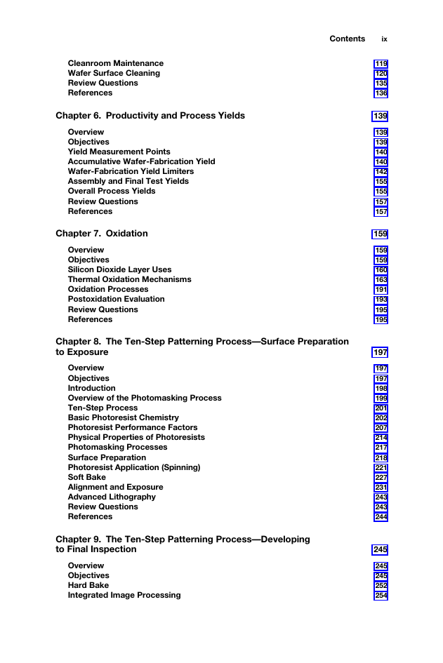
5.7 Cleanroom Maintenance
5.8 Wafer Surface Cleaning
5.9 Review Questions
5.10 References
6. Productivity and Process Yields
6.1 Overview
6.2 Objectives
6.3 Yield Measurement Points
6.4 Accumulative Wafer-Fabrication Yield
6.5 Wafer-Fabrication Yield Limiters
6.6 Assembly and Final Test Yields
6.7 Overall Process Yields
6.8 Review Questions
6.9 References
7. Oxidation
7.1 Overview
7.2 Objectives
7.3 Silicon Dioxide Layer Uses
7.4 Thermal Oxidation Mechanisms
7.5 Oxidation Processes
7.6 Postoxidation Evaluation
7.7 Review Questions
7.8 References
8. The Ten-Step Patterning Process - Surface Preparation to Exposure
8.1 Overview
8.2 Objectives
8.3 Introduction
8.4 Overview of the Photomasking Process
8.5 Ten-Step Process
8.6 Basic Photoresist Chemistry
8.7 Photoresist Performance Factors
8.8 Physical Properties of Photoresists
8.9 Photomasking Processes
8.10 Surface Preparation
8.11 Photoresist Application (Spinning)
8.12 Soft Bake
8.13 Alignment and Exposure
8.14 Advanced Lithography
8.15 Review Questions
8.16 References
9. The Ten-Step Patterning Process - Developing to Final Inspection
9.1 Overview
9.2 Objectives
9.3 Hard Bake
9.4 Integrated Image Processing
9.5 Etch
9.6 Wet Etching
9.7 Dry Etch
9.8 Resist Stripping
9.9 Final Inspection
9.10 Mask Making
9.11 Summary
9.12 Review Questions
9.13 References
10. Advanced Photolithography Processes
10.1 Overview
10.2 Objectives
10.3 Issues of VLSI/ULSI Patterning
10.4 Other Exposure Issues
10.5 Surface Problems
10.6 Antireflective Coatings
10.7 Photoresist Process Advances
10.8 Improving Etch Definition
10.9 Self-Aligned Structures
10.10 Etch Profile Control
10.11 Review Questions
10.12 References
11. Doping
11.1 Overview
11.2 Objectives
11.3 Introduction
11.4 Formation of a Doped Region by Diffusion
11.5 Formation of a Doped Region and Junction by Diffusion
11.6 Diffusion Process Steps
11.7 Deposition
11.8 Drive-in Oxidation
11.9 Introduction to Ion Implantation
11.10 Concept of Ion Implantation
11.11 Ion Implantation System
11.12 Dopant Concentration in Implanted Regions
11.13 Evaluation of Implanted Layers
11.14 Uses of Ion Implantation
11.15 The Future of Doping
11.16 Review Questions
11.17 References
12. Layer Deposition
12.1 Overview
12.2 Objectives
12.3 Introduction
12.4 Chemical Vapor Deposition Basics
12.5 CVD Process Steps
12.6 CVD System Types
12.7 Atmospheric-Pressure CVD Systems
12.8 Low-Pressure Chemical Vapor Deposition (LPCVD)
12.9 Atomic Layer Deposition (ALD)
12.10 Vapor Phase Epitaxy (VPE)
12.11 Molecular Beam Epitaxy (MBE)
12.12 Metalorganic CVD (MOCVD)
12.13 Deposited Films
12.14 Deposited Semiconductors
12.15 Epitaxial Silicon
12.16 Polysilicon and Amorphous Silicon Deposition
12.17 SOS and SOI
12.18 Gallium Arsenide on Silicon
12.19 Insulators and Dielectrics
12.20 Conductors
12.21 Review Questions
12.22 References
13. Metallization
13.1 Overview
13.2 Objectives
13.3 Introduction
13.4 Conductors - Single-Level Metal
13.5 Conductors - Multilevel Metal Schemes
13.6 Conductors
13.7 Electrochemical Plating (ECP)
13.8 Chemical Mechanical Processing
13.9 Metal Film Uses
13.10 Deposition Methods
13.11 Vacuum Pumps
13.12 Summary
13.13 Review Questions
13.14 References
14. Process and Device Evaluation
14.1 Overview
14.2 Objectives
14.3 Introduction
14.4 Wafer Electrical Measurements
14.5 Process and Device Evaluation
14.6 Physical Measurement Methods
14.7 Layer Thickness Measurements
14.8 Junction Depth
14.9 Contamination and Defect Detection
14.10 General Surface Characterization
14.11 Contamination Identification
14.12 Device Electrical Measurements
14.13 Review Questions
14.14 References
15. The Business of Wafer Fabrication
15.1 Overview
15.2 Objectives
15.3 Wafer Fabrication Costs
15.4 Equipment
15.5 Automation
15.6 Factory-Level Automation
15.7 Equipment Standards
15.8 Statistical Process Control (SPC)
15.9 Inventory Control
15.10 Quality Control and Certification - ISO 9000
15.11 Line Organization
15.12 Review Questions
15.13 References
16. Introduction to Devices and Integrated Circuit Formation
16.1 Overview
16.2 Objectives
16.3 Semiconductor-Device Formation
16.4 Alternative (Scaled) Transistor Designs
16.5 Integrated-Circuit Formation
16.6 Bi-MOS
16.7 Superconductors
16.8 Review Questions
16.9 References
17. Introduction to Integrated Circuits
17.1 Overview
17.2 Objectives
17.3 Introduction
17.4 Circuit Basics
17.5 Integrated Circuit Types
17.6 The Next Generation
17.7 Review Questions
17.8 References
18. Packaging
18.1 Overview
18.2 Objectives
18.3 Introduction
18.4 Chip Characteristics
18.5 Package Functions and Design
18.6 Overview of Packaging Operations
18.7 Packaging Processes
18.8 Alternative Process
18.9 Transfer to Packaging Area
18.10 Package Process Flows
18.11 Package/Bare Die Strategies
18.12 Package Design
18.13 Package Type/Technology Summary
18.14 Review Questions
18.15 References
Glossary
Index
A
B
C
D
E
F
G
H
I
J
K
L
M
N
O
P
Q
R
S
T
U
V
W
X
Y
Z
32418_01.pdf
Front Matter
Table of Contents
1. The Semiconductor Industry
1.1 Overview
1.2 Objectives
1.3 Birth of an Industry
1.4 The Solid-State Era
1.5 Integrated Circuits (ICs)
1.6 Process and Product Trends
1.7 Industry Organization
1.8 Stages of Manufacturing
1.9 The Junction Transistor
1.10 Five Decades of Industry Development
1.11 The Nano Era
1.12 Review Questions
1.13 References
Index
A
B
C
D
E
F
G
H
I
J
K
L
M
N
O
P
Q
R
S
T
U
V
W
X
Y
Z
32418_02.pdf
Front Matter
Table of Contents
2. Properties of Semiconductor Materials and Chemicals
2.1 Overview
2.2 Objectives
2.3 Atomic Structure
2.4 The Periodic Table of the Elements
2.5 Electrical Conduction
2.6 Dielectrics and Capacitors
2.7 Intrinsic Semiconductors
2.8 Doped Semiconductors
2.9 Electron and Hole Conduction
2.10 Semiconductor Production Materials
2.11 Semiconducting Compounds
2.12 Silicon Germanium
2.13 Engineered Substrates
2.14 Ferroelectric Materials
2.15 Diamond Semiconductors
2.16 Process Chemicals
2.17 States of Matter
2.18 Properties of Matter
2.19 Pressure and Vacuum
2.20 Acids, Alkalis, and Solvents
2.21 Chemical Purity and Cleanliness
2.22 Review Questions
2.23 References
Index
A
B
C
D
E
F
G
H
I
J
K
L
M
N
O
P
Q
R
S
T
U
V
W
X
Y
Z
32418_03.pdf
Front Matter
Table of Contents
3. Crystal Growth and Silicon Wafer Preparation
3.1 Overview
3.2 Objectives
3.3 Introduction
3.4 Semiconductor Silicon Preparation
3.5 Crystalline Materials
3.6 Crystal Orientation
3.7 Crystal Growth
3.8 Crystal and Wafer Quality
3.9 Wafer Preparation
3.10 Wafer Slicing
3.11 Wafer Marking
3.12 Rough Polish
3.13 Chemical Mechanical Polishing (CMP)
3.14 Backside Processing
3.15 Double-Sided Polishing
3.16 Edge Grinding and Polishing
3.17 Wafer Evaluation
3.18 Oxidation
3.19 Packaging
3.20 Engineered Wafers (Substrates)
3.21 Review Questions
3.22 References
Index
A
B
C
D
E
F
G
H
I
J
K
L
M
N
O
P
Q
R
S
T
U
V
W
X
Y
Z
32418_04.pdf
Front Matter
Table of Contents
4. Overview of Wafer Fabrication
4.1 Overview
4.2 Objectives
4.3 Goal of Wafer Fabrication
4.4 Wafer Terminology
4.5 Basic Wafer-Fabrication Operations
4.6 Example Fabrication Process
4.7 Chip Terminology
4.8 Wafer Sort
4.9 Packaging
4.10 Summary
4.11 Review Questions
4.12 References
Index
A
B
C
D
E
F
G
H
I
J
K
L
M
N
O
P
Q
R
S
T
U
V
W
X
Y
Z
32418_05.pdf
Front Matter
Table of Contents
5. Contamination Control
5.1 Overview
5.2 Objectives
5.3 Introduction
5.4 Contamination Sources
5.5 Cleanroom Construction
5.6 Cleanroom Materials and Supplies
5.7 Cleanroom Maintenance
5.8 Wafer Surface Cleaning
5.9 Review Questions
5.10 References
Index
A
B
C
D
E
F
G
H
I
J
K
L
M
N
O
P
Q
R
S
T
U
V
W
X
Y
Z
32418_06.pdf
Front Matter
Table of Contents
6. Productivity and Process Yields
6.1 Overview
6.2 Objectives
6.3 Yield Measurement Points
6.4 Accumulative Wafer-Fabrication Yield
6.5 Wafer-Fabrication Yield Limiters
6.6 Assembly and Final Test Yields
6.7 Overall Process Yields
6.8 Review Questions
6.9 References
Index
A
B
C
D
E
F
G
H
I
J
K
L
M
N
O
P
Q
R
S
T
U
V
W
X
Y
Z
32418_07.pdf
Front Matter
Table of Contents
7. Oxidation
7.1 Overview
7.2 Objectives
7.3 Silicon Dioxide Layer Uses
7.4 Thermal Oxidation Mechanisms
7.5 Oxidation Processes
7.6 Postoxidation Evaluation
7.7 Review Questions
7.8 References
Index
A
B
C
D
E
F
G
H
I
J
K
L
M
N
O
P
Q
R
S
T
U
V
W
X
Y
Z
32418_08.pdf
Front Matter
Table of Contents
8. The Ten-Step Patterning Process - Surface Preparation to Exposure
8.1 Overview
8.2 Objectives
8.3 Introduction
8.4 Overview of the Photomasking Process
8.5 Ten-Step Process
8.6 Basic Photoresist Chemistry
8.7 Photoresist Performance Factors
8.8 Physical Properties of Photoresists
8.9 Photomasking Processes
8.10 Surface Preparation
8.11 Photoresist Application (Spinning)
8.12 Soft Bake
8.13 Alignment and Exposure
8.14 Advanced Lithography
8.15 Review Questions
8.16 References
Index
A
B
C
D
E
F
G
H
I
J
K
L
M
N
O
P
Q
R
S
T
U
V
W
X
Y
Z
32418_09.pdf
Front Matter
Table of Contents
9. The Ten-Step Patterning Process - Developing to Final Inspection
9.1 Overview
9.2 Objectives
9.3 Hard Bake
9.4 Integrated Image Processing
9.5 Etch
9.6 Wet Etching
9.7 Dry Etch
9.8 Resist Stripping
9.9 Final Inspection
9.10 Mask Making
9.11 Summary
9.12 Review Questions
9.13 References
Index
A
B
C
D
E
F
G
H
I
J
K
L
M
N
O
P
Q
R
S
T
U
V
W
X
Y
Z
32418_10.pdf
Front Matter
Table of Contents
10. Advanced Photolithography Processes
10.1 Overview
10.2 Objectives
10.3 Issues of VLSI/ULSI Patterning
10.4 Other Exposure Issues
10.5 Surface Problems
10.6 Antireflective Coatings
10.7 Photoresist Process Advances
10.8 Improving Etch Definition
10.9 Self-Aligned Structures
10.10 Etch Profile Control
10.11 Review Questions
10.12 References
Index
A
B
C
D
E
F
G
H
I
J
K
L
M
N
O
P
Q
R
S
T
U
V
W
X
Y
Z
32418_11.pdf
Front Matter
Table of Contents
11. Doping
11.1 Overview
11.2 Objectives
11.3 Introduction
11.4 Formation of a Doped Region by Diffusion
11.5 Formation of a Doped Region and Junction by Diffusion
11.6 Diffusion Process Steps
11.7 Deposition
11.8 Drive-in Oxidation
11.9 Introduction to Ion Implantation
11.10 Concept of Ion Implantation
11.11 Ion Implantation System
11.12 Dopant Concentration in Implanted Regions
11.13 Evaluation of Implanted Layers
11.14 Uses of Ion Implantation
11.15 The Future of Doping
11.16 Review Questions
11.17 References
Index
A
B
C
D
E
F
G
H
I
J
K
L
M
N
O
P
Q
R
S
T
U
V
W
X
Y
Z
32418_12.pdf
Front Matter
Table of Contents
12. Layer Deposition
12.1 Overview
12.2 Objectives
12.3 Introduction
12.4 Chemical Vapor Deposition Basics
12.5 CVD Process Steps
12.6 CVD System Types
12.7 Atmospheric-Pressure CVD Systems
12.8 Low-Pressure Chemical Vapor Deposition (LPCVD)
12.9 Atomic Layer Deposition (ALD)
12.10 Vapor Phase Epitaxy (VPE)
12.11 Molecular Beam Epitaxy (MBE)
12.12 Metalorganic CVD (MOCVD)
12.13 Deposited Films
12.14 Deposited Semiconductors
12.15 Epitaxial Silicon
12.16 Polysilicon and Amorphous Silicon Deposition
12.17 SOS and SOI
12.18 Gallium Arsenide on Silicon
12.19 Insulators and Dielectrics
12.20 Conductors
12.21 Review Questions
12.22 References
Index
A
B
C
D
E
F
G
H
I
J
K
L
M
N
O
P
Q
R
S
T
U
V
W
X
Y
Z
32418_13.pdf
Front Matter
Table of Contents
13. Metallization
13.1 Overview
13.2 Objectives
13.3 Introduction
13.4 Conductors - Single-Level Metal
13.5 Conductors - Multilevel Metal Schemes
13.6 Conductors
13.7 Electrochemical Plating (ECP)
13.8 Chemical Mechanical Processing
13.9 Metal Film Uses
13.10 Deposition Methods
13.11 Vacuum Pumps
13.12 Summary
13.13 Review Questions
13.14 References
Index
A
B
C
D
E
F
G
H
I
J
K
L
M
N
O
P
Q
R
S
T
U
V
W
X
Y
Z
32418_14.pdf
Front Matter
Table of Contents
14. Process and Device Evaluation
14.1 Overview
14.2 Objectives
14.3 Introduction
14.4 Wafer Electrical Measurements
14.5 Process and Device Evaluation
14.6 Physical Measurement Methods
14.7 Layer Thickness Measurements
14.8 Junction Depth
14.9 Contamination and Defect Detection
14.10 General Surface Characterization
14.11 Contamination Identification
14.12 Device Electrical Measurements
14.13 Review Questions
14.14 References
Index
A
B
C
D
E
F
G
H
I
J
K
L
M
N
O
P
Q
R
S
T
U
V
W
X
Y
Z
32418_15.pdf
Front Matter
Table of Contents
15. The Business of Wafer Fabrication
15.1 Overview
15.2 Objectives
15.3 Wafer Fabrication Costs
15.4 Equipment
15.5 Automation
15.6 Factory-Level Automation
15.7 Equipment Standards
15.8 Statistical Process Control (SPC)
15.9 Inventory Control
15.10 Quality Control and Certification - ISO 9000
15.11 Line Organization
15.12 Review Questions
15.13 References
Index
A
B
C
D
E
F
G
H
I
J
K
L
M
N
O
P
Q
R
S
T
U
V
W
X
Y
Z
32418_16.pdf
Front Matter
Table of Contents
16. Introduction to Devices and Integrated Circuit Formation
16.1 Overview
16.2 Objectives
16.3 Semiconductor-Device Formation
16.4 Alternative (Scaled) Transistor Designs
16.5 Integrated-Circuit Formation
16.6 Bi-MOS
16.7 Superconductors
16.8 Review Questions
16.9 References
Index
A
B
C
D
E
F
G
H
I
J
K
L
M
N
O
P
Q
R
S
T
U
V
W
X
Y
Z
32418_17.pdf
Front Matter
Table of Contents
17. Introduction to Integrated Circuits
17.1 Overview
17.2 Objectives
17.3 Introduction
17.4 Circuit Basics
17.5 Integrated Circuit Types
17.6 The Next Generation
17.7 Review Questions
17.8 References
Index
A
B
C
D
E
F
G
H
I
J
K
L
M
N
O
P
Q
R
S
T
U
V
W
X
Y
Z
32418_18.pdf
Front Matter
Table of Contents
18. Packaging
18.1 Overview
18.2 Objectives
18.3 Introduction
18.4 Chip Characteristics
18.5 Package Functions and Design
18.6 Overview of Packaging Operations
18.7 Packaging Processes
18.8 Alternative Process
18.9 Transfer to Packaging Area
18.10 Package Process Flows
18.11 Package/Bare Die Strategies
18.12 Package Design
18.13 Package Type/Technology Summary
18.14 Review Questions
18.15 References
Index
A
B
C
D
E
F
G
H
I
J
K
L
M
N
O
P
Q
R
S
T
U
V
W
X
Y
Z
32418_glo.pdf
Front Matter
Table of Contents
Glossary
Index
A
B
C
D
E
F
G
H
I
J
K
L
M
N
O
P
Q
R
S
T
U
V
W
X
Y
Z
32418_indx.pdf
Front Matter
Table of Contents
Index
A
B
C
D
E
F
G
H
I
J
K
L
M
N
O
P
Q
R
S
T
U
V
W
X
Y
Z



 2023年江西萍乡中考道德与法治真题及答案.doc
 2012年重庆南川中考生物真题及答案.doc
 2013年江西师范大学地理学综合及文艺理论基础考研真题.doc
 2020年四川甘孜小升初语文真题及答案I卷.doc
 2020年注册岩土工程师专业基础考试真题及答案.doc
 2023-2024学年福建省厦门市九年级上学期数学月考试题及答案.doc
 2021-2022学年辽宁省沈阳市大东区九年级上学期语文期末试题及答案.doc
 2022-2023学年北京东城区初三第一学期物理期末试卷及答案.doc
 2018上半年江西教师资格初中地理学科知识与教学能力真题及答案.doc
 2012年河北国家公务员申论考试真题及答案-省级.doc
 2020-2021学年江苏省扬州市江都区邵樊片九年级上学期数学第一次质量检测试题及答案.doc
 2022下半年黑龙江教师资格证中学综合素质真题及答案.doc