acam-messelectronic gmbH
is now
Member of the
ams Group
The technical content of this acam-messelectronic document is still valid.
Contact information:
Headquarters:
ams AG
Tobelbaderstrasse 30
8141 Unterpremstaetten, Austria
Tel: +43 (0) 3136 500 0
e-Mail: ams_sales@ams.com
Please visit our website at www.ams.com
�
®
Data Sheet
PCapØ2A
Single-chip Solution for Capacitance Measurement
Volume 1: General Data and Front-end Description
May 29, 2014, Version 1.6
Document-No: DB_PCapØ2A_Vol1_en.pdf
Member of the ams Group�
®
PCapØ2A
P u b l i s h e d b y a c a m - m e s s e l e c t r o n i c g m b h
©acam-messelectronic gmbh 2014
L i m i t a t i o n o f L i a b i l i t y / W a r r a n t y / C o p y r i g h t
The information and data contained in this document are believed to be accurate and
reliable. acam assumes no liability for errors and gives no warranty representation or
guarantee regarding the suitability of its products for any particular purpose due to these
specifications. Any information and data which may be provided in the document can and
do vary in different applications, and actual performance may vary over time. All operating
parameters must be validated for each customer application by customers’ technical
experts.
The information contained therein may be protected by copyright, patent, trademark
and/or other intellectual property rights of acam. acam does not assume responsibility for
patent infringements or other rights of third parties which may result from its use.
acam reserves the right to review this document and to make changes to the document’s
content at any time without obligation to notify any person or entity of such revision or
changes. “Preliminary” product information describes a product which is not in full
production so that full information about the product is not available yet.
Do not use our products in life-supporting systems, aviation and aerospace applications!
Unless explicitly agreed to otherwise in writing between the parties, acam’ products are
not designed, intended or authorized for use as components in systems intended for
surgical implants into the body, or other applications intended to support or sustain life, or
for any other application in which the failure of the product could create a situation where
personal injury or death could occur.
No part of this publication may be reproduced, photocopied, stored on a retrieval system
or transmitted without the express written consent of acam.
All rights not expressly granted remain reserved by acam., , and
are registered trademarks of acam. All other brand and product names in this
document are trademarks or service marks of their respective owners.
S u p p o r t / C o n t a c t
For a complete listing of Direct Sales, Distributor and Sales Representative contacts, visit
the acam web site at:
http://www.acam.de/sales/distributors/
For technical support you can contact the acam support team in the headquarters in
Germany or the Distributor in your country. The contact details of acam in Germany are:
support@acam.de
or by phone
+49-7244-74190.
acam messelectronic gmbh - Friedrich-List-Str.4 - 76297 Stutensee - Germany - www.acam.de
Member of the ams Group�
PCapØ2A
Content
1 Overview .................................................................................................. 1-1
1.1
Features ............................................................................................. 1-1
1.2 Applications ........................................................................................ 1-2
1.3 Blockdiagram ...................................................................................... 1-2
2 Characteristics & Specifications ................................................................... 2-1
2.1
Electrical Characteristics ....................................................................... 2-1
2.2 CDC Precision ..................................................................................... 2-2
2.3 RDC Precision ..................................................................................... 2-3
2.4 Oscillators .......................................................................................... 2-4
2.5 Power Consumption .............................................................................. 2-1
2.6 Package Information ............................................................................. 2-2
2.7 QFN Packages ..................................................................................... 2-4
3 Converter Frontend .................................................................................... 3-1
3.1 CDC, Capacitance-to-Digital Converter ...................................................... 3-1
3.2 CDC Compensation Options .................................................................... 3-7
3.3 CDC Important Parameters .................................................................... 3-9
3.4 RDC Resistance-to-Digital Converter ...................................................... 3-12
3.5 RDC Important Parameters .................................................................. 3-15
4
Interfaces (Serial & PDM/PWM) .................................................................. 4-1
4.1
4.2
4.3
4.4
Serial Interfaces................................................................................... 4-1
I²C Compatible Interface ........................................................................ 4-2
SPI interface ....................................................................................... 4-3
Special Timings .................................................................................... 4-5
4.5 OTP Timings ........................................................................................ 4-7
4.6 GPIO and PDM/PWM ......................................................................... 4-10
4.7
Interfaces Parameters ........................................................................ 4-15
5 Configuration & Read Registers .................................................................... 5-1
5.1 Configuration registers .......................................................................... 5-1
5.2 Configuration Registers in Detail ............................................................. 5-4
5.3 Oscillator Configuration ....................................................................... 5-20
5.4
Low Battery Detection (LBD) ................................................................ 5-21
5.5 Read Registers .................................................................................. 5-22
6 DSP & Memory.......................................................................................... 6-1
6.1 Memory Map ....................................................................................... 6-2
6.2 Memory Management ........................................................................... 6-3
6.3 Getting started .................................................................................... 6-5
acam messelectronic gmbh - Friedrich-List-Str.4 - 76297 Stutensee - Germany - www.acam.de
1
Member of the ams Group�
®
PCapØ2A
7 Miscellaneous ........................................................................................... 7-1
7.1 Bug Report ......................................................................................... 7-1
7.2
7.3
I²C Bug with POR directly after rd/wr OTP/SRAM ...................................... 7-1
Limitation of Parameter2 ....................................................................... 7-1
7.4 History ............................................................................................... 7-2
2
acam messelectronic gmbh - Friedrich-List-Str.4 - 76297 Stutensee - Germany - www.acam.de
Member of the ams Group�
PCapØ2A
1 Overview
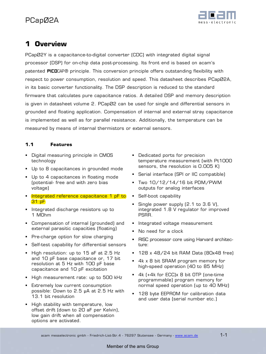
PCapØ2Y is a capacitance-to-digital converter (CDC) with integrated digital signal
processor (DSP) for on-chip data post-processing. Its front end is based on acam‘s
patented ® principle. This conversion principle offers outstanding flexibility with
respect to power consumption, resolution and speed. This datasheet describes PCapØ2A,
in its basic converter functionality. The DSP description is reduced to the standard
firmware that calculates pure capacitance ratios. A detail ed DSP and memory description
is given in datasheet volume 2. PCapØ2 can be used for single and differential sensors in
grounded and floating application. Compensation of internal and external stray capacitance
is implemented as well as for parallel resistance. Additionally, the temperature can be
measured by means of internal thermistors or external sensors.
1.1
Features
Digital measuring principle in CMOS
Dedicated ports for precision
technology
Up to 8 capacitances in grounded mode
Up to 4 capacitances in floating mode
temperature measurement (with Pt1000
sensors, the resolution is 0.005 K)
Serial interface (SPI or IIC compatible)
(potential- free and with zero bias
voltage)
Two 10/12/14/16 bit PDM/PWM
outputs for analog interfaces
Integrated reference capacitance 1 pF to
31 pF
Integrated discharge resistors up to
1 MOhm
Self-boot capability
Single power supply (2.1 to 3.6 V),
integrated 1.8 V regulator for improved
PSRR.
Compensation of internal (grounded) and
Integrated voltage measurement
external parasitic capacities (floating)
Pre-charge option for slow charging
No need for a clock
RISC processor core using Harvard architec-
Self-test capability for differential sensors
ture:
High resolution: up to 15 aF at 2.5 Hz
and 10 pF base capacitance or, 17 bit
resolution at 5 Hz with 100 pF base
capacitance and 10 pF excitation
High measurement rate: up to 500 kHz
Extremely low current consumption
possible: Down to 2.5 μA at 2.5 Hz with
13.1 bit resolution
High stability with temperature, low
offset drift (down to 20 aF per Kelvin),
low gain drift when all compensation
options are activated.
128 x 48/24 bit RAM Data (80x48 free)
4k x 8 bit SRAM program memory for
high-speed operation (40 to 85 MHz)
4k (+4k for ECC)x 8 bit OTP (one-time
programmable) program memory for
normal speed operation (up to 40 MHz)
128 byte EEPROM for calibration data
and user data (serial number etc.)
acam messelectronic gmbh - Friedrich-List-Str.4 - 76297 Stutensee - Germany - www.acam.de
1-1
Member of the ams Group�
PCapØ2A
Tilt sensors
Angle sensors
Wireless applications
Level sensors
Microphones
MEMS sensors
®
1.2
应用
Humidity sensors
Position sensors
Pressure sensors
Force sensors
Acceleration sensors
Inclination sensors
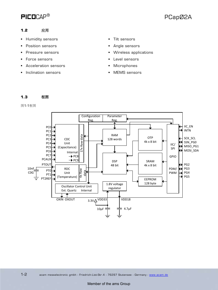
1.3
框图
图1-1框图
1-2
acam messelectronic gmbh - Friedrich-List-Str.4 - 76297 Stutensee - Germany - www.acam.de
RDCUnit(Temperature)4x Raw dataCDCUnit(Capacitance)17x Raw dataRAM128 wordsDSP48 bitConfigurationReg. ParameterReg. OTP4k x 8 bitSRAM4k x 8 bitEEPROM128 byte1.8V voltageregulatorOscillator Control UnitExt. Quartz InternalIIC/SPIGPIOPDM/PWMPC0PC1PC2PC3PC4PC5PC6PC7PCAUXPT0PT1PT2REFIIC_ENINTNSCK_SCLSSN_PG0MISO_PG1MOSI_SDAPG2PG3PG4PG5VDD18VDD33OXIN OXOUTInternal:PC8PC910µF4.7µFPTOUT10nFC0G3.3VMember of the ams Group�
PCapØ2A
2 Characteristics & Specifications
2.1
Electrical Characteristics
2.1.1
Absolute Maximum Ratings
Supply voltage VDD-to-GND
- 0.3 to 4.0 V
Storage temperature Tstg
- 55 to 150 °C
ESD rating (HBM), each pin
> 2 kV
Junction temperature (Tj)
max. 125 °C
OTP Data Retention Period
10 years at 95 °C temperature
EEPROM Data Retention Period
10 years at 95 °C temperature
2.1.2
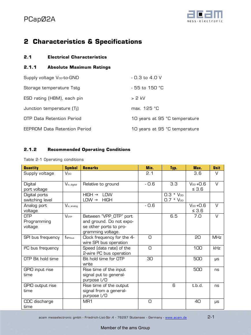
Recommended Operating Conditions
Table 2-1 Operating conditions
Quantity
Supply voltage
Symbol Remarks
VDD
Min.
2.1
Typ.
Max.
3.6
Unit
V
Vio_digital
Relative to ground
- 0.6
3.3
VDD +0.6
V
HIGH LOW
LOW HIGH
Between “VPP_OTP” port
and ground. Do not expo-
se other ports to pro-
gramming voltage.
Clock frequency for the 4-
wire SPI bus operation
Speed (data rate) of the
2-wire I²C bus operation
Bit hold time for OTP
write
Rise time of the input
signal put to general-
purpose I/O
Rise time of the output
signal from a general-
purpose I/O
MR1
≤ 3.6
0.3 * VDD
0.7 * VDD
- 0.6
VDD +0.6
≤ 3.6
7.0
V
V
6.5
0
0
30
20
MHz
100
kHz
500
500
μs
ns
6
t.b.d.
ns
0
40
µs
Digital
port voltage
Digital ports
switching level
Analog port
voltage
OTP
Programming
voltage
Vio_analog
VOTP
SPI bus frequency
fSPI-bus
I²C bus frequency
OTP Bit hold time
GPIO input rise
time
GPIO output rise
time
CDC discharge
time
acam messelectronic gmbh - Friedrich-List-Str.4 - 76297 Stutensee - Germany - www.acam.de
2-1
Member of the ams Group�




 2023年江西萍乡中考道德与法治真题及答案.doc
 2012年重庆南川中考生物真题及答案.doc
 2013年江西师范大学地理学综合及文艺理论基础考研真题.doc
 2020年四川甘孜小升初语文真题及答案I卷.doc
 2020年注册岩土工程师专业基础考试真题及答案.doc
 2023-2024学年福建省厦门市九年级上学期数学月考试题及答案.doc
 2021-2022学年辽宁省沈阳市大东区九年级上学期语文期末试题及答案.doc
 2022-2023学年北京东城区初三第一学期物理期末试卷及答案.doc
 2018上半年江西教师资格初中地理学科知识与教学能力真题及答案.doc
 2012年河北国家公务员申论考试真题及答案-省级.doc
 2020-2021学年江苏省扬州市江都区邵樊片九年级上学期数学第一次质量检测试题及答案.doc
 2022下半年黑龙江教师资格证中学综合素质真题及答案.doc