BCM2837 ARM Peripherals
V2.1
Revised edition by FA on 2018/03/20 partially based on the valuable errata information available in:
https://elinux.org/BCM2835_datasheet_errata and starting from a previous updated document done
by a professor at Stanford: https://web.stanford.edu/class/cs140e/docs/BCM2837-ARM-Peripherals.pdf
© 2012 Broadcom Corporation.
All rights reserved
Broadcom Europe Ltd. 406 Science Park Milton Road Cambridge CB4 0WW
�
Table of Contents
Introduction
Overview
Address map
1
1.1
1.2
1.2.1
1.2.2
1.2.3
1.2.4
1.3
Diagrammatic overview
ARM virtual addresses (standard Linux kernel only)
ARM physical addresses
Bus addresses
Peripheral access precautions for correct memory ordering
Overview
Mini UART
AUX registers
2 Auxiliaries: UART1 & SPI1, SPI2
2.1
2.1.1
2.2
2.2.1
2.2.2
2.3
2.3.1
2.3.2
2.3.3
2.3.4
SPI implementation details
Interrupts
Long bit streams
SPI register details.
Universal SPI Master (2x)
Mini UART implementation details.
Mini UART register details.
3 BSC
3.1
3.2
3.3
Introduction
Register View
10 Bit Addressing
Overview
DMA Controller Registers
4 DMA Controller
4.1
4.2
4.2.1
4.3
4.4
4.5
AXI Bursts
Error Handling
DMA LITE Engines
DMA Channel Register Address Map
5
o
o
External Mass Media Controller
Introduction
Registers
6 General Purpose I/O (GPIO)
6.1
6.2
6.3
Register View
Alternative Function Assignments
General Purpose GPIO Clocks
7
7.1
7.2
7.3
7.4
7.5
Interrupts
Introduction
Interrupt pending.
Fast Interrupt (FIQ).
Interrupt priority.
Registers
PCM / I2S Audio
Block Diagram
Typical Timing
Operation
Software Operation
8
8.1
8.2
8.3
8.4
8.4.1
8.4.2
06 February 2012 Broadcom Europe Ltd. 406 Science Park Milton Road Cambridge CB4 0WW
Operating in Polled mode
Operating in Interrupt mode
© 2012 Broadcom Corporation. All rights reserved
4
4
4
4
6
6
6
7
8
8
9
10
11
11
20
20
21
21
22
28
28
28
36
38
38
39
40
63
63
63
65
65
66
89
90
102
105
109
109
110
110
110
112
119
120
120
121
122
122
123
Page ii
�
8.4.3
8.5
8.6
8.7
8.8
DMA
Error Handling.
PDM Input Mode Operation
GRAY Code Input Mode Operation
PCM Register Map
9
9.1
9.2
9.3
9.4
9.5
9.6
Pulse Width Modulator
Overview
Block Diagram
PWM Implementation
Modes of Operation
Quick Reference
Control and Status Registers
10 SPI
10.1
10.2
10.2.1
10.2.2
10.3
10.3.1
10.3.2
10.3.3
10.3.4
10.3.5
10.4
10.5
10.6
10.6.1
10.6.2
10.6.3
10.6.4
Introduction
SPI Master Mode
Standard mode
Bidirectional mode
LoSSI mode
Command write
Parameter write
Byte read commands
24bit read command
32bit read command
Block Diagram
SPI Register Map
Software Operation
Polled
Interrupt
DMA
Notes
11 SPI/BSC SLAVE
11.1
Introduction
11.2
Registers
12 System Timer
12.1
System Timer Registers
13 UART
13.1
13.2
13.3
13.4
Variations from the 16C650 UART
Primary UART Inputs and Outputs
UART Interrupts
Register View
14 Timer (ARM side)
14.1
14.2
Introduction
Timer Registers:
15 USB
15.1
15.2
Configuration
Extra / Adapted registers.
123
123
124
124
125
138
138
138
139
139
140
141
148
148
148
148
149
150
150
150
151
151
151
152
152
158
158
158
158
159
160
160
160
172
172
175
175
176
176
177
196
196
196
200
200
202
06 February 2012 Broadcom Europe Ltd. 406 Science Park Milton Road Cambridge CB4 0WW
Page iii
© 2012 Broadcom Corporation. All rights reserved
�
1
Introduction
1.1 Overview
BCM2835 contains the following peripherals which may safely be accessed by the ARM:
Interrupt controller
• Timers
•
• GPIO
• USB
• PCM / I2S
• DMA controller
•
•
• SPI0, SPI1, SPI2
• PWM
• UART0, UART1
I2C master
I2C / SPI slave
The purpose of this datasheet is to provide documentation for these peripherals in sufficient
detail to allow a developer to port an operating system to BCM2835.
There are a number of peripherals which are intended to be controlled by the GPU. These are
omitted from this datasheet. Accessing these peripherals from the ARM is not recommended.
1.2 Address map
1.2.1 Diagrammatic overview
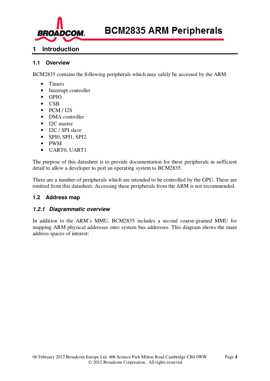
In addition to the ARM’s MMU, BCM2835 includes a second coarse-grained MMU for
mapping ARM physical addresses onto system bus addresses. This diagram shows the main
address spaces of interest:
06 February 2012 Broadcom Europe Ltd. 406 Science Park Milton Road Cambridge CB4 0WW
Page 4
© 2012 Broadcom Corporation. All rights reserved
�
06 February 2012 Broadcom Europe Ltd. 406 Science Park Milton Road Cambridge CB4 0WW
Page 5
© 2012 Broadcom Corporation. All rights reserved
�
Addresses in ARM Linux are:
issued as virtual addresses by the ARM core, then
•
• mapped into a physical address by the ARM MMU, then
• mapped into a bus address by the ARM mapping MMU, and finally
• used to select the appropriate peripheral or location in RAM.
1.2.2 ARM virtual addresses (standard Linux kernel only)
As is standard practice, the standard BCM2835 Linux kernel provides a contiguous mapping
over the whole of available RAM at the top of memory. The kernel is configured for a
1GB/3GB split between kernel and user-space memory.
The split between ARM and GPU memory is selected by installing one of the supplied
start*.elf files as start.elf in the FAT32 boot partition of the SD card. The minimum amount
of memory which can be given to the GPU is 32MB, but that will restrict the multimedia
performance; for example, 32MB does not provide enough buffering for the GPU to do
1080p30 video decoding.
Virtual addresses in kernel mode will range between 0xC0000000 and 0xEFFFFFFF.
Virtual addresses in user mode (i.e. seen by processes running in ARM Linux) will range
between 0x00000000 and 0xBFFFFFFF.
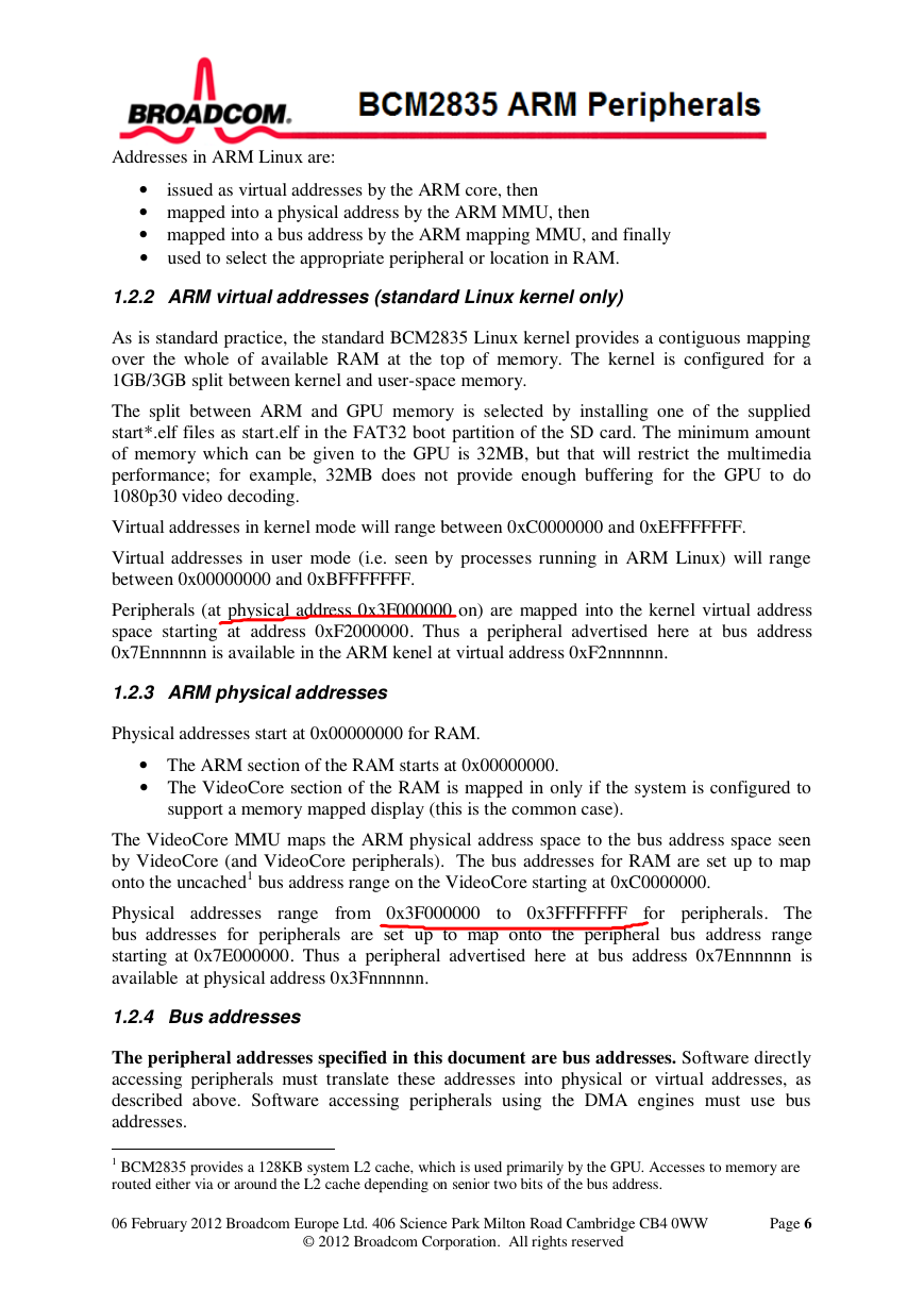
Peripherals (at physical address 0x3F000000 on) are mapped into the kernel virtual address
space starting at address 0xF2000000. Thus a peripheral advertised here at bus address
0x7Ennnnnn is available in the ARM kenel at virtual address 0xF2nnnnnn.
1.2.3 ARM physical addresses
Physical addresses start at 0x00000000 for RAM.
• The ARM section of the RAM starts at 0x00000000.
• The VideoCore section of the RAM is mapped in only if the system is configured to
support a memory mapped display (this is the common case).
The VideoCore MMU maps the ARM physical address space to the bus address space seen
by VideoCore (and VideoCore peripherals). The bus addresses for RAM are set up to map
onto the uncached1 bus address range on the VideoCore starting at 0xC0000000.
Physical addresses range from 0x3F000000 to 0x3FFFFFFF for peripherals. The
bus addresses for peripherals are set up to map onto the peripheral bus address range
starting at 0x7E000000. Thus a peripheral advertised here at bus address 0x7Ennnnnn is
available at physical address 0x3Fnnnnnn.
1.2.4 Bus addresses
The peripheral addresses specified in this document are bus addresses. Software directly
accessing peripherals must translate these addresses into physical or virtual addresses, as
described above. Software accessing peripherals using the DMA engines must use bus
addresses.
1 BCM2835 provides a 128KB system L2 cache, which is used primarily by the GPU. Accesses to memory are
routed either via or around the L2 cache depending on senior two bits of the bus address.
06 February 2012 Broadcom Europe Ltd. 406 Science Park Milton Road Cambridge CB4 0WW
Page 6
© 2012 Broadcom Corporation. All rights reserved
�
Software accessing RAM directly must use physical addresses (based at 0x00000000).
Software accessing RAM using the DMA engines must use bus addresses (based at
0xC0000000).
1.3 Peripheral access precautions for correct memory ordering
The BCM2835 system uses an AMBA AXI-compatible interface structure. In order to keep
the system complexity low and data throughput high, the BCM2835 AXI system does not
always return read data in-order2. The GPU has special logic to cope with data arriving out-
of-order; however the ARM core does not contain such logic. Therefore some precautions
must be taken when using the ARM to access peripherals.
Accesses to the same peripheral will always arrive and return in-order. It is only when
switching from one peripheral to another that data can arrive out-of-order. The simplest way
to make sure that data is processed in-order is to place a memory barrier instruction at critical
positions in the code. You should place:
• A memory write barrier before the first write to a peripheral.
• A memory read barrier after the last read of a peripheral.
It is not required to put a memory barrier instruction after each read or write access. Only at
those places in the code where it is possible that a peripheral read or write may be followed
by a read or write of a different peripheral. This is normally at the entry and exit points of the
peripheral service code.
As interrupts can appear anywhere in the code so you should safeguard those. If an interrupt
routine reads from a peripheral the routine should start with a memory read barrier. If an
interrupt routine writes to a peripheral the routine should end with a memory write barrier.
2Normally a processor assumes that if it executes two read operations the data will arrive in order. So a read
from location X followed by a read from location Y should return the data of location X first, followed by the
data of location Y. Data arriving out of order can have disastrous consequences. For example:
a_status = *pointer_to_peripheral_a;
b_status = *pointer_to_peripheral_b;
Without precautions the values ending up in the variables a_status and b_status can be swapped around.
It is theoretical possible for writes to go ‘wrong’ but that is far more difficult to achieve. The AXI system
makes sure the data always arrives in-order at its intended destination. So:
*pointer_to_peripheral_a = value_a;
*pointer_to_peripheral_b = value_b;
will always give the expected result. The only time write data can arrive out-of-order is if two different
peripherals are connected to the same external equipment.
06 February 2012 Broadcom Europe Ltd. 406 Science Park Milton Road Cambridge CB4 0WW
Page 7
© 2012 Broadcom Corporation. All rights reserved
�
2 Auxiliaries: UART1 & SPI1, SPI2
2.1 Overview
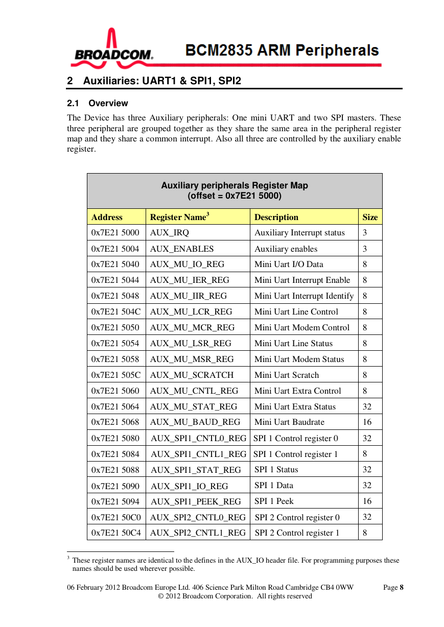
The Device has three Auxiliary peripherals: One mini UART and two SPI masters. These
three peripheral are grouped together as they share the same area in the peripheral register
map and they share a common interrupt. Also all three are controlled by the auxiliary enable
register.
Auxiliary peripherals Register Map
(offset = 0x7E21 5000)
Address
Register Name3
Description
Size
0x7E21 5000 AUX_IRQ
Auxiliary Interrupt status
0x7E21 5004 AUX_ENABLES
Auxiliary enables
0x7E21 5040 AUX_MU_IO_REG
Mini Uart I/O Data
0x7E21 5044 AUX_MU_IER_REG
Mini Uart Interrupt Enable
3
3
8
8
0x7E21 5048 AUX_MU_IIR_REG
Mini Uart Interrupt Identify 8
0x7E21 504C AUX_MU_LCR_REG
Mini Uart Line Control
0x7E21 5050 AUX_MU_MCR_REG
Mini Uart Modem Control
0x7E21 5054 AUX_MU_LSR_REG
Mini Uart Line Status
0x7E21 5058 AUX_MU_MSR_REG
Mini Uart Modem Status
0x7E21 505C AUX_MU_SCRATCH
Mini Uart Scratch
0x7E21 5060 AUX_MU_CNTL_REG Mini Uart Extra Control
0x7E21 5064 AUX_MU_STAT_REG Mini Uart Extra Status
0x7E21 5068 AUX_MU_BAUD_REG Mini Uart Baudrate
0x7E21 5080 AUX_SPI1_CNTL0_REG SPI 1 Control register 0
0x7E21 5084 AUX_SPI1_CNTL1_REG SPI 1 Control register 1
0x7E21 5088 AUX_SPI1_STAT_REG
SPI 1 Status
0x7E21 5090 AUX_SPI1_IO_REG
SPI 1 Data
0x7E21 5094 AUX_SPI1_PEEK_REG
SPI 1 Peek
0x7E21 50C0 AUX_SPI2_CNTL0_REG SPI 2 Control register 0
0x7E21 50C4 AUX_SPI2_CNTL1_REG SPI 2 Control register 1
8
8
8
8
8
8
32
16
32
8
32
32
16
32
8
3 These register names are identical to the defines in the AUX_IO header file. For programming purposes these
names should be used wherever possible.
06 February 2012 Broadcom Europe Ltd. 406 Science Park Milton Road Cambridge CB4 0WW
Page 8
© 2012 Broadcom Corporation. All rights reserved
�



 2023年江西萍乡中考道德与法治真题及答案.doc
 2012年重庆南川中考生物真题及答案.doc
 2013年江西师范大学地理学综合及文艺理论基础考研真题.doc
 2020年四川甘孜小升初语文真题及答案I卷.doc
 2020年注册岩土工程师专业基础考试真题及答案.doc
 2023-2024学年福建省厦门市九年级上学期数学月考试题及答案.doc
 2021-2022学年辽宁省沈阳市大东区九年级上学期语文期末试题及答案.doc
 2022-2023学年北京东城区初三第一学期物理期末试卷及答案.doc
 2018上半年江西教师资格初中地理学科知识与教学能力真题及答案.doc
 2012年河北国家公务员申论考试真题及答案-省级.doc
 2020-2021学年江苏省扬州市江都区邵樊片九年级上学期数学第一次质量检测试题及答案.doc
 2022下半年黑龙江教师资格证中学综合素质真题及答案.doc