< Dual-In-Line Package Intelligent Power Module >
PSS25SA2FT
INSULATED TYPE
TRANSFER MOLDING TYPE
OUTLINE
MAIN FEATURES AND RATINGS
● 3 phase DC/AC inverter
● 1200V / 25A
● Built-in LPT-CSTBT (6th generation IGBT)
● Built-in bootstrap diodes with current limiting resistor
● Insulated transfer molding package
● N-side IGBT open emitter
APPLICATION
● AC 400V class motor control
: Drive circuit, High voltage high-speed level shifting, Control supply under-voltage (UV) protection
: Drive circuit, Control supply under-voltage protection (UV), Short circuit protection (SC)
INTEGRATED DRIVE, PROTECTION AND SYSTEM CONTROL FUNCTIONS
● For P-side
● For N-side
● Fault signaling : Corresponding to SC fault (N-side IGBT), UV fault (N-side supply)
● Temperature output : Outputting LVIC temperature by analog signal
● Input interface : 5V line, Schmitt trigger receiver circuit (High Active)
● UL Recognized : UL1557 File E80276
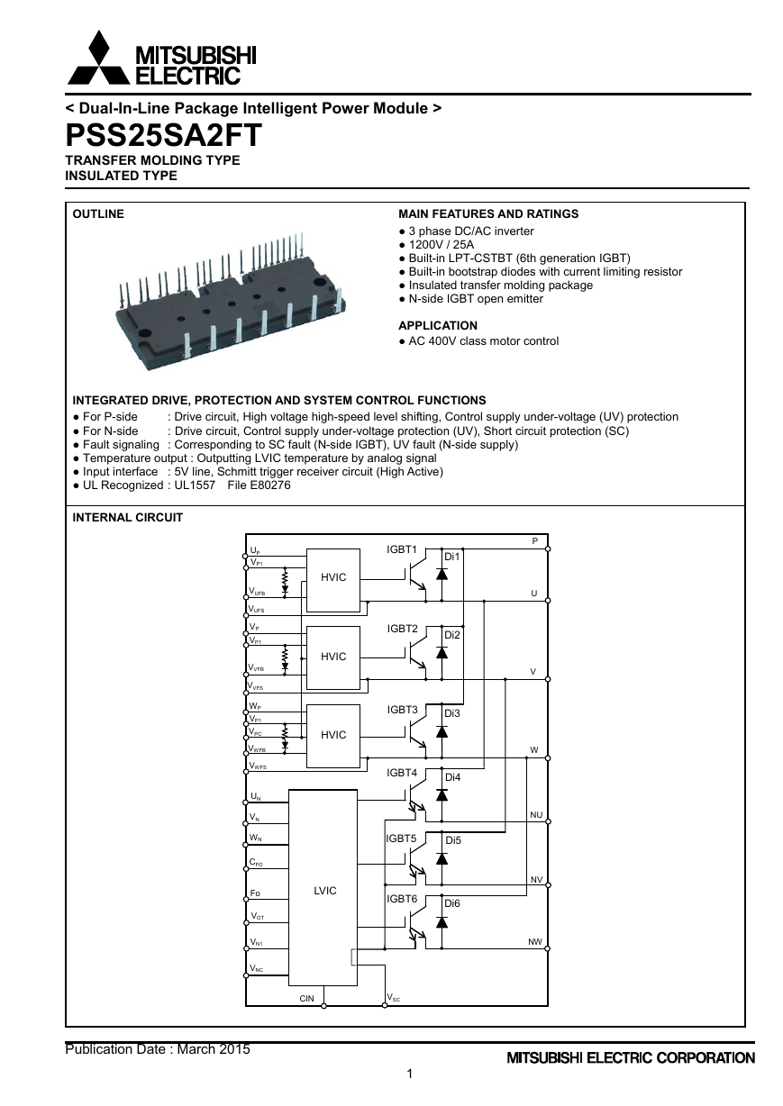
INTERNAL CIRCUIT
HVIC
HVIC
HVIC
IGBT1
Di1
IGBT2
Di2
IGBT3
Di3
IGBT4
Di4
IGBT5
Di5
LVIC
IGBT6
Di6
UP
VP1
VUFB
VUFS
VP
VP1
VVFB
VVFS
WP
VP1
VPC
VWFB
VWFS
UN
VN
WN
CFO
Fo
VOT
VN1
VNC
P
U
V
W
NU
NV
NW
Publication Date : March 2015
CIN
VSC
1
�
< Dual-In-Line Package Intelligent Power Module >
PSS25SA2FT
TRANSFER MOLDING TYPE
INSULATED TYPE
MAXIMUM RATINGS (Tj = 25°C, unless otherwise noted)
INVERTER PART
Parameter
Supply voltage
Supply voltage (surge)
Collector-emitter voltage
Each IGBT collector current
Each IGBT collector current (peak)
Collector dissipation
Junction temperature
Symbol
VCC
VCC(surge)
VCES
±IC
±ICP
PC
Tj
Note 1: Pulse width and period are limited due to junction temperature.
CONTROL (PROTECTION) PART
Parameter
Control supply voltage
Control supply voltage
Input voltage
Fault output supply voltage
Fault output current
Current sensing input voltage
Symbol
VD
VDB
VIN
VFO
IFO
VSC
Condition
Applied between P-NU,NV,NW
Applied between P-NU,NV,NW
TC= 25°C (Note 1)
TC= 25°C, up to 1ms
TC= 25°C, per 1 chip
Ratings
900
1000
1200
25
50
103
-30~+150
Condition
Applied between VP1-VPC, VN1-VNC
Applied between VUFB-VUFS, VVFB-VVFS, VWFB-VWFS
Applied between UP, VP, WP-VPC, UN, VN, WN-VNC
Applied between FO-VNC
Sink current at FO terminal
Applied between CIN-VNC
Unit
V
V
V
A
A
W
°C
Unit
V
V
V
V
mA
V
Unit
V
°C
°C
Vrms
Ratings
20
20
-0.5~VD+0.5
-0.5~VD+0.5
5
-0.5~VD+0.5
Ratings
800
-30~+100
-40~+125
2500
TOTAL SYSTEM
Parameter
Symbol
VCC(PROT) Self protection supply voltage limit
(Short circuit protection capability)
Module case operation temperature
TC
Storage temperature
Tstg
Viso
Isolation voltage
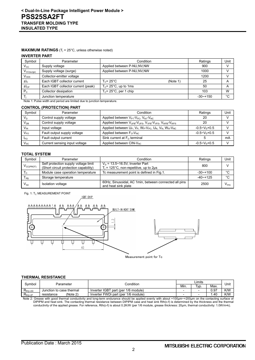
Fig. 1: TC MEASUREMENT POINT
Condition
VD = 13.5~16.5V, Inverter Part
Tj = 125°C, non-repetitive, up to 2μs
Tc measurement point is defined in Fig.1.
60Hz, Sinusoidal, AC 1min, between connected all pins
and heat sink plate
THERMAL RESISTANCE
Measurement point for Tc
Parameter
Condition
Symbol
Rth(j-c)Q
Rth(j-c)F
Note 2: Grease with good thermal conductivity and long-term endurance should be applied evenly with about +100μm~+200μm on the contacting surface of
DIPIPM and heat sink. The contacting thermal resistance between DIPIPM case and heat sink Rth(c-f) is determined by the thickness and the thermal
conductivity of the applied grease. For reference, Rth(c-f) is about 0.2K/W (per 1/6 module, grease thickness: 20μm, thermal conductivity: 1.0W/m•k).
Inverter IGBT part (per 1/6 module)
Inverter FWDi part (per 1/6 module)
Junction to case thermal
resistance (Note 2)
Unit
K/W
K/W
Max.
0.97
1.40
Min.
-
-
Limits
Typ.
-
-
Publication Date : March 2015
2
�
< Dual-In-Line Package Intelligent Power Module >
PSS25SA2FT
TRANSFER MOLDING TYPE
INSULATED TYPE
ELECTRICAL CHARACTERISTICS (Tj = 25°C, unless otherwise noted)
INVERTER PART
Symbol
Parameter
Condition
VCE(sat)
VEC
ton
tC(on)
toff
tC(off)
trr
ICES
Collector-emitter saturation
voltage
FWDi forward voltage
VD=VDB = 15V, VIN= 5V, IC= 25A
VIN= 0V, -IC= 25A
Tj= 25°C
Tj= 125°C
Switching times
VCC= 600V, VD= VDB= 15V
IC= 25A, Tj= 125°C, VIN= 0↔5V
Inductive Load (upper-lower arm)
Collector-emitter cut-off
current
VCE=VCES
Tj= 25°C
Tj= 125°C
CONTROL (PROTECTION) PART
Symbol
Parameter
ID
IDB
ISC
Circuit current
Short circuit trip level
Condition
VD=15V, VIN=0V
VD=15V, VIN=5V
VDB=15V, VIN=0V
VDB=15V, VIN=5V
Total of VP1-VPC, VN1-VNC
Each part of VUFB-VUFS,
VVFB-VVFS, VWFB-VWFS
-30°C≤Tj≤125°C, Rs=75Ω (±1%),
Not connecting outer shunt resistors to
NU,NV,NW terminals
Limits
Typ.
1.50
1.70
2.20
1.90
0.50
2.60
0.50
0.50
-
-
Min.
-
-
-
1.10
-
-
-
-
-
-
Limits
Typ.
Min.
-
-
-
-
(Note 3)
42.5
-
-
-
-
-
Unit
V
V
μs
μs
μs
μs
μs
mA
Unit
mA
Max.
2.20
2.40
2.80
2.60
0.80
3.60
0.90
-
1
10
Max.
5.60
5.60
1.10
1.10
-
A
Tj ≤125°C
Tj ≤125°C
Fault output voltage
Trip level
Reset level
Trip level
Reset level
P-side Control supply
under-voltage
protection(UV)
N-side Control supply
under-voltage
protection(UV)
UVDBt
UVDBr
UVDt
UVDr
VFOH
VFOL
tFO
IIN
Vth(on)
Vth(off)
VOT
VF
R
Note 3: Short circuit protection detects sense current divided from main current at N-side IGBT and works for N-side IGBT only. In the case that outer shunt resistor is
Fault output pulse width
Input current
ON threshold voltage
OFF threshold voltage
Temperature output
Bootstrap Di forward voltage
Built-in limiting resistance
VSC = 0V, FO terminal pulled up to 5V by 10kΩ
VSC = 1V, IFO = 1mA
CFO=22nF
VIN = 5V
LVIC temperature = 75°C
IF=10mA including voltage drop by limiting resistor
Included in bootstrap Di
-
-
-
-
-
-
2.4
1.00
10.0
10.5
10.3
10.8
4.9
-
1.6
0.70
-
0.8
2.26
0.5
16
Applied between UP, VP, WP, UN, VN, WN-VNC
V
V
V
V
V
V
ms
mA
(Note 5)
(Note 6)
12.0
12.5
12.5
13.0
-
-
0.95
1.50
3.5
-
2.51
1.3
24
-
-
2.38
0.9
20
inserted into main current path, protection current level ISC changes. For details, please refer the application note for this DIPIPM.
Note 4: Fault signal is output when short circuit or N-side control supply under-voltage protection works. The fault output pulse-width tFO depends on the capacitance of
V
V
V
Ω
(Note 4)
CFO. (CFO (typ.) = tFO x 9.1 x 10⁻⁶) [F])
Note 5: DIPIPM doesn't shut down IGBTs and output fault signal automatically when temperature rises excessively. When temperature exceeds the protective level that
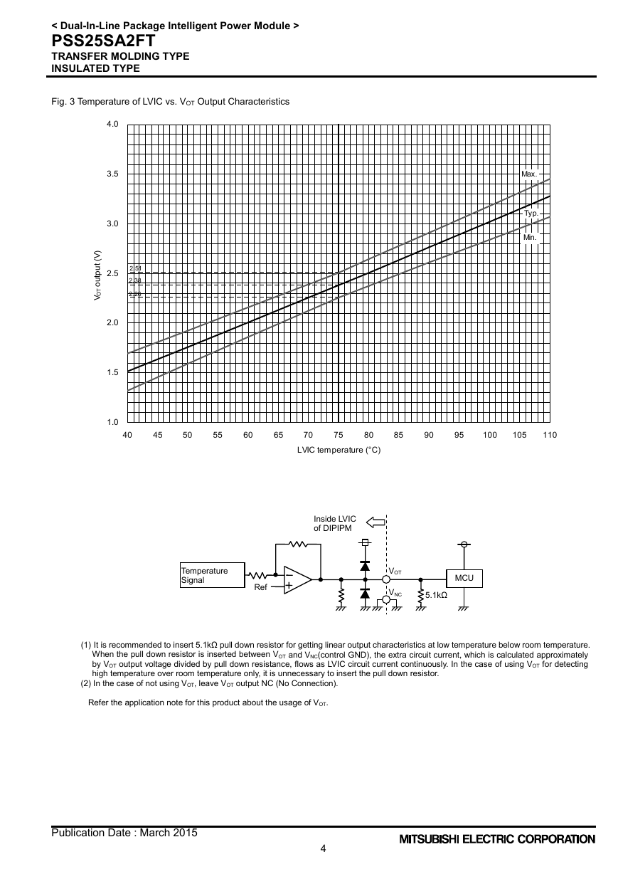
user defined, controller (MCU) should stop immediately. Temperature of LVIC vs. VOT output characteristics is described in Fig.3
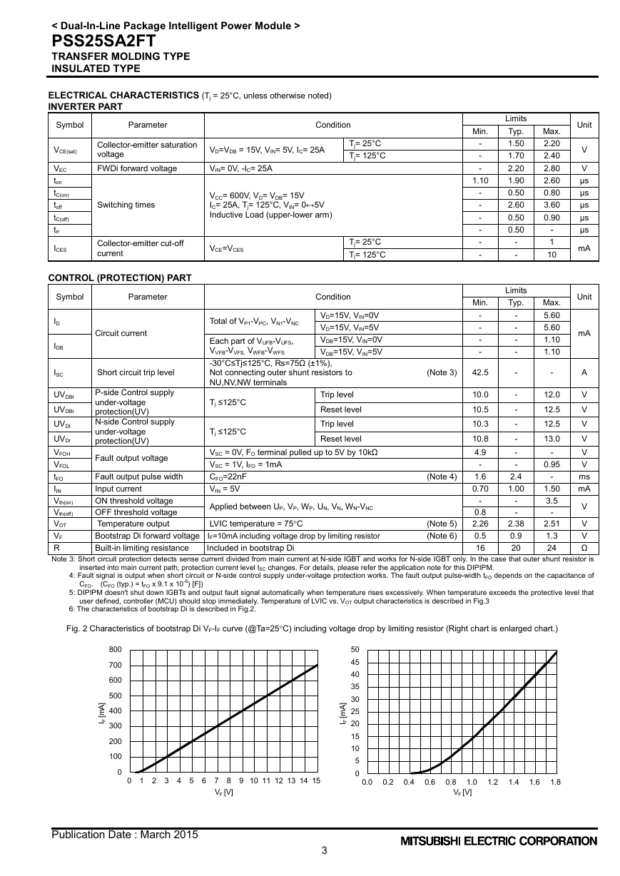
Note 6: The characteristics of bootstrap Di is described in Fig.2.
Fig. 2 Characteristics of bootstrap Di VF-IF curve (@Ta=25°C) including voltage drop by limiting resistor (Right chart is enlarged chart.)
]
A
m
[
F
I
800
700
600
500
400
300
200
100
0
0 1 2 3 4 5 6 7 8 9 10 11 12 13 14 15
VF [V]
Publication Date : March 2015
3
]
A
m
[
F
I
50
45
40
35
30
25
20
15
10
5
0
0.0 0.2 0.4 0.6 0.8 1.0 1.2 1.4 1.6 1.8
VF [V]
�
< Dual-In-Line Package Intelligent Power Module >
PSS25SA2FT
TRANSFER MOLDING TYPE
INSULATED TYPE
Fig. 3 Temperature of LVIC vs. VOT Output Characteristics
_
)
V
(
t
t
u
p
u
o
T
O
V
4.0
3.5
3.0
2.5
2.0
1.5
1.0
2.51
2.38
2.26
Max.
Typ.
Min.
40
45
50
55
60
65
70
75
80
85
90
95
100
105
110
LVIC temperature (°C)
Inside LVIC
of DIPIPM
Temperature
Signal
Ref
VOT
VNC
MCU
5.1kΩ
(1) It is recommended to insert 5.1kΩ pull down resistor for getting linear output characteristics at low temperature below room temperature.
When the pull down resistor is inserted between VOT and VNC(control GND), the extra circuit current, which is calculated approximately
by VOT output voltage divided by pull down resistance, flows as LVIC circuit current continuously. In the case of using VOT for detecting
high temperature over room temperature only, it is unnecessary to insert the pull down resistor.
(2) In the case of not using VOT, leave VOT output NC (No Connection).
Refer the application note for this product about the usage of VOT.
Publication Date : March 2015
4
�
< Dual-In-Line Package Intelligent Power Module >
PSS25SA2FT
TRANSFER MOLDING TYPE
INSULATED TYPE
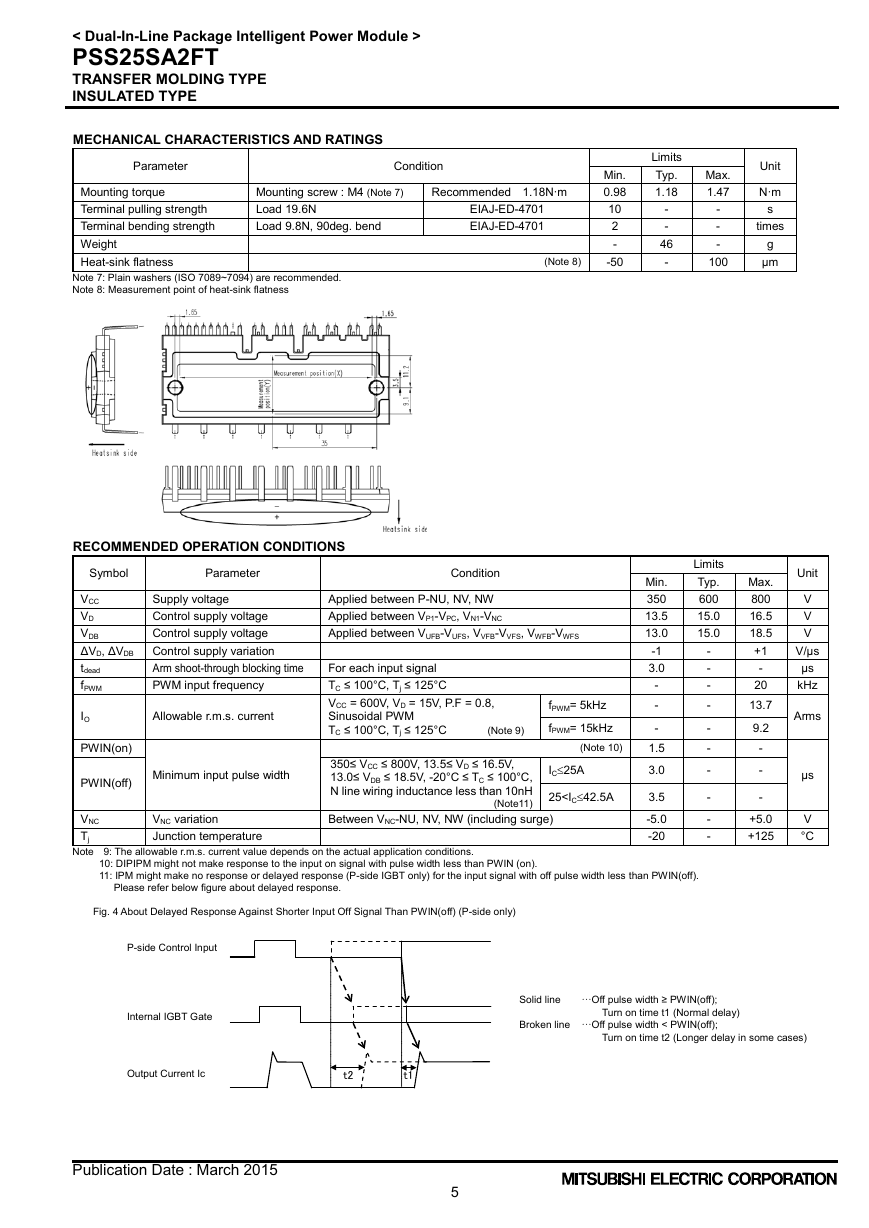
MECHANICAL CHARACTERISTICS AND RATINGS
Parameter
Mounting torque
Terminal pulling strength
Terminal bending strength
Weight
Heat-sink flatness
Condition
Mounting screw : M4 (Note 7)
Load 19.6N
Load 9.8N, 90deg. bend
Recommended 1.18N·m
EIAJ-ED-4701
EIAJ-ED-4701
(Note 8)
Limits
Typ.
1.18
-
-
46
-
Min.
0.98
10
2
-
-50
Max.
1.47
-
-
-
100
Unit
N·m
s
times
g
μm
Note 7: Plain washers (ISO 7089~7094) are recommended.
Note 8: Measurement point of heat-sink flatness
RECOMMENDED OPERATION CONDITIONS
Symbol
Parameter
Condition
VCC
Supply voltage
VD
Control supply voltage
VDB
Control supply voltage
ΔVD, ΔVDB Control supply variation
tdead
fPWM
Arm shoot-through blocking time
PWM input frequency
IO
Allowable r.m.s. current
PWIN(on)
PWIN(off)
Minimum input pulse width
Applied between P-NU, NV, NW
Applied between VP1-VPC, VN1-VNC
Applied between VUFB-VUFS, VVFB-VVFS, VWFB-VWFS
For each input signal
TC ≤ 100°C, Tj ≤ 125°C
VCC = 600V, VD = 15V, P.F = 0.8,
Sinusoidal PWM
TC ≤ 100°C, Tj ≤ 125°C (Note 9)
350≤ VCC ≤ 800V, 13.5≤ VD ≤ 16.5V,
13.0≤ VDB ≤ 18.5V, -20°C ≤ TC ≤ 100°C,
N line wiring inductance less than 10nH
(Note11)
IC≤25A
fPWM= 5kHz
fPWM= 15kHz
(Note 10)
25
< Dual-In-Line Package Intelligent Power Module >
PSS25SA2FT
TRANSFER MOLDING TYPE
INSULATED TYPE
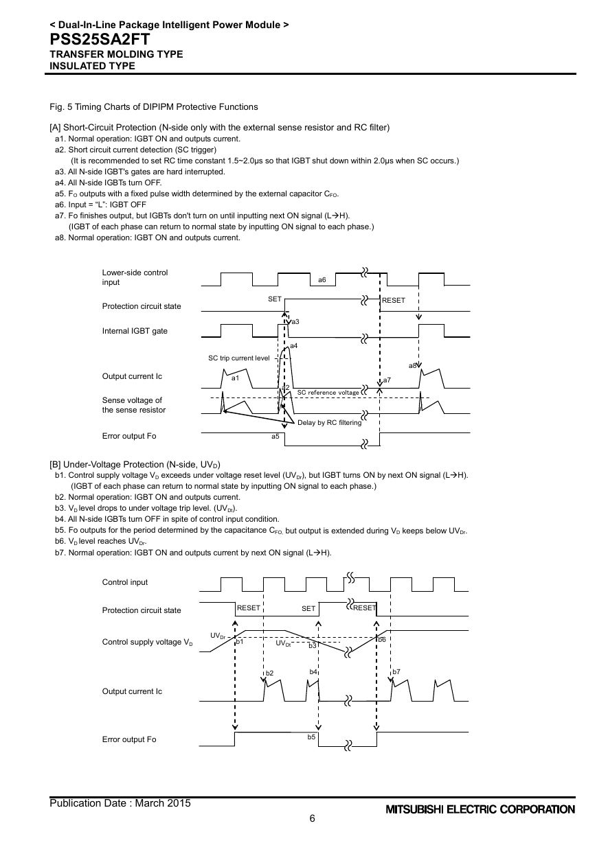
Fig. 5 Timing Charts of DIPIPM Protective Functions
[A] Short-Circuit Protection (N-side only with the external sense resistor and RC filter)
a1. Normal operation: IGBT ON and outputs current.
a2. Short circuit current detection (SC trigger)
(It is recommended to set RC time constant 1.5~2.0μs so that IGBT shut down within 2.0μs when SC occurs.)
a3. All N-side IGBT's gates are hard interrupted.
a4. All N-side IGBTs turn OFF.
a5. FO outputs with a fixed pulse width determined by the external capacitor CFO.
a6. Input = “L”: IGBT OFF
a7. Fo finishes output, but IGBTs don't turn on until inputting next ON signal (LH).
(IGBT of each phase can return to normal state by inputting ON signal to each phase.)
a8. Normal operation: IGBT ON and outputs current.
a6
Internal IGBT gate
SET
RESET
Protection circuit state
Lower-side control
input
[B] Under-Voltage Protection (N-side, UVD)
b1. Control supply voltage VD exceeds under voltage reset level (UVDr), but IGBT turns ON by next ON signal (LH).
Sense voltage of
the sense resistor
a2
SC reference voltage
a8
a7
Output current Ic
a1
Error output Fo
a5
a3
a4
SC trip current level
Delay by RC filtering
(IGBT of each phase can return to normal state by inputting ON signal to each phase.)
b2. Normal operation: IGBT ON and outputs current.
b3. VD level drops to under voltage trip level. (UVDt).
b4. All N-side IGBTs turn OFF in spite of control input condition.
b5. Fo outputs for the period determined by the capacitance CFO, but output is extended during VD keeps below UVDr.
b6. VD level reaches UVDr.
b7. Normal operation: IGBT ON and outputs current by next ON signal (LH).
Control input
Protection circuit state
RESET
SET
RESET
Control supply voltage VD
UVDr
b1
UVDt
b2
Output current Ic
Error output Fo
b6
b7
b3
b4
b5
6
Publication Date : March 2015
�
< Dual-In-Line Package Intelligent Power Module >
PSS25SA2FT
TRANSFER MOLDING TYPE
INSULATED TYPE
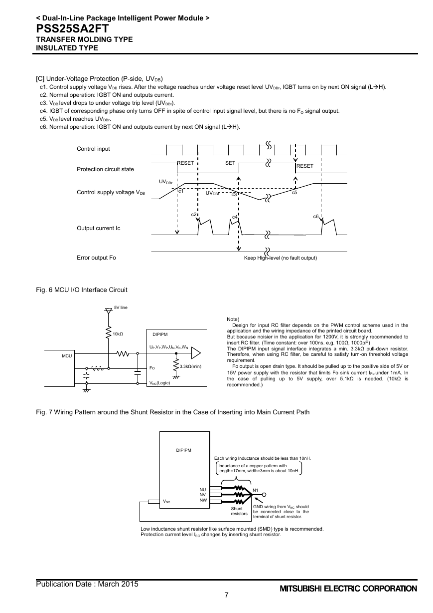
[C] Under-Voltage Protection (P-side, UVDB)
c1. Control supply voltage VDB rises. After the voltage reaches under voltage reset level UVDBr, IGBT turns on by next ON signal (LH).
c2. Normal operation: IGBT ON and outputs current.
c3. VDB level drops to under voltage trip level (UVDBt).
c4. IGBT of corresponding phase only turns OFF in spite of control input signal level, but there is no FO signal output.
c5. VDB level reaches UVDBr.
c6. Normal operation: IGBT ON and outputs current by next ON signal (LH).
RESET
c6
Keep High-level (no fault output)
5V line
Control input
Error output Fo
UVDBt
c3
c5
c2
c4
UVDBr
c1
RESET
SET
Output current Ic
Protection circuit state
Control supply voltage VDB
Fig. 6 MCU I/O Interface Circuit
Fig. 7 Wiring Pattern around the Shunt Resistor in the Case of Inserting into Main Current Path
Inductance of a copper pattern with
length=17mm, width=3mm is about 10nH.
GND wiring from VNC should
be connected close to the
terminal of shunt resistor.
Fo
3.3kΩ(min)
10kΩ
DIPIPM
NU
NV
NW
VNC
N1
Shunt
resistors
DIPIPM
Each wiring Inductance should be less than 10nH.
UP,VP,WP,UN,VN,WN
VNC(Logic)
MCU
Note)
Design for input RC filter depends on the PWM control scheme used in the
application and the wiring impedance of the printed circuit board.
But because noisier in the application for 1200V, it is strongly recommended to
insert RC filter. (Time constant: over 100ns. e.g. 100Ω, 1000pF)
The DIPIPM input signal interface integrates a min. 3.3kΩ pull-down resistor.
Therefore, when using RC filter, be careful to satisfy turn-on threshold voltage
requirement.
Fo output is open drain type. It should be pulled up to the positive side of 5V or
15V power supply with the resistor that limits Fo sink current IFo under 1mA. In
the case of pulling up to 5V supply, over 5.1kΩ is needed. (10kΩ is
recommended.)
Low inductance shunt resistor like surface mounted (SMD) type is recommended.
Protection current level ISC changes by inserting shunt resistor.
Publication Date : March 2015
7
�
< Dual-In-Line Package Intelligent Power Module >
PSS25SA2FT
TRANSFER MOLDING TYPE
INSULATED TYPE
Fig. 8 Example of Application Circuit
M
C
U
HVIC
HVIC
HVIC
LVIC
R3
C5
C2
+
C1 D1 C2
R3
C5
C2
+
C1 D1 C2
R3
C5
C2
+
C1 D1 C2
R3
C5
R3
C5
R3
C5
5V
R2
15V
VD
+
D1
C1
C2
UP(1)
VP1(3)
VUFB(4)
VUFS(6)
VP(7)
VP1(9)
VVFB(10)
VVFS(12)
WP(13)
VP1(14)
VPC(15)
VWFB(16)
VWFS(18)
UN(27)
VN(28)
WN(29)
CFO(25)
Fo(26)
VOT(23)
VN1(21)
VNC(22)
CIN(24)
C4
B
R1
IGBT1
Di1
IGBT2
Di2
IGBT3
Di3
IGBT4
Di4
IGBT5
Di5
IGBT6
Di6
VSC(19)
D
Sense
resistor
A
P(40)
U(39)
V(38)
M
W(37)
NU (36)
NV (35)
NW(34)
C
+
C3
Note
1 :If control GND and power GND are patterned by common wiring, it may cause malfunction by fluctuation of power GND level. It is recommended to connect
Control GND wiring
Power GND wiring
N1
control GND and power GND at only a N1 point at which NU, NV, NW are connected to power GND line.
2 :It is recommended to insert a Zener diode D1 (24V/1W) between each pair of control supply terminals to prevent surge destruction.
3 :To prevent surge destruction, the wiring between the smoothing capacitor and the P, N1 terminals should be as short as possible. Generally inserting a
0.1μ~0.22μF snubber capacitor C3 between the P-N1 terminals is recommended.
4 :R1, C4 of RC filter for preventing protection circuit malfunction is recommended to select tight tolerance, temp-compensated type. The time constant R1C4
should be set so that SC current is shut down within 2μs. (1.5μs~2μs is general value.) SC interrupting time might vary with the wiring pattern, so the enough
evaluation on the real system is recommended. If R1 is too small, it may leads to delay of protection. So R1 should be min. 10 times larger resistance than Rs.
(100 times is recommended.)
5 :To prevent erroneous operation, the wiring of A, B, C should be as short as possible.
6 :For sense resistor, the variation within 1%(including temperature characteristics), low inductance type is recommended. And the over 0.03W is recommended,
8 :All capacitors should be mounted as close to the terminals of the DIPIPM as possible. (C1: good temperature, frequency characteristic electrolytic type, and
C2: 0.01μ~2.0μF, good temperature, frequency and DC bias characteristic ceramic type are recommended.)
9 :Input drive is High-active type. There is a min. 3.3kΩ pull-down resistor in the input circuit of IC. To prevent malfunction, the wiring of each input should be as
short as possible. And it is recommended to insert RC filter (e.g. R3=100Ω and C5=1000pF) and confirm the input signal level to meet the turn-on and turn-off
threshold voltage. Thanks to HVIC inside the module, direct coupling to MCU without any opto-coupler or transformer isolation is possible.
10 :Fo output is open drain type. Fo output will be max 0.95V(@IFO=1mA,25℃), so it should be pulled up to MCU or control power supply (e.g. 5V,15V) by a
resistor that makes IFo up to 1mA. (In the case of pulled up to 5V, 10kΩ is recommended.)
11 :Error signal output width (tFo) can be set by the capacitor connected to CFO terminal. CFO(typ.) = tFo x 9.1 x 10⁻⁶ (F)
12 :If high frequency noise superimposed to the control supply line, IC malfunction might happen and cause erroneous operation. To avoid such problem, voltage
ripple of control supply line should meet dV/dt ≤+/-1V/μs, Vripple≤2Vp-p.
13 :For DIPIPM, it isn't recommended to drive same load by parallel connection with other phase IGBT or other DIPIPM.
7 :To prevent erroneous SC protection, the wiring from VSC terminal to CIN filter should be divided at the point D that is close to the terminal of sense resistor.
but it is necessary to evaluate in your real system finally.
And the wiring should be patterned as short as possible.
Publication Date : March 2015
8
�


 2023年江西萍乡中考道德与法治真题及答案.doc
 2012年重庆南川中考生物真题及答案.doc
 2013年江西师范大学地理学综合及文艺理论基础考研真题.doc
 2020年四川甘孜小升初语文真题及答案I卷.doc
 2020年注册岩土工程师专业基础考试真题及答案.doc
 2023-2024学年福建省厦门市九年级上学期数学月考试题及答案.doc
 2021-2022学年辽宁省沈阳市大东区九年级上学期语文期末试题及答案.doc
 2022-2023学年北京东城区初三第一学期物理期末试卷及答案.doc
 2018上半年江西教师资格初中地理学科知识与教学能力真题及答案.doc
 2012年河北国家公务员申论考试真题及答案-省级.doc
 2020-2021学年江苏省扬州市江都区邵樊片九年级上学期数学第一次质量检测试题及答案.doc
 2022下半年黑龙江教师资格证中学综合素质真题及答案.doc