Analysis and Design of Single-Phase Current-Source Grid-Connected PV Inverter
G. Ertasgin
BILECIK SEYH EDEBALI UNIVERSITY
Bilecik, Turkey
gurhan.ertasgin@bilecik.edu.tr
W.L. Soong and N. Ertugrul
THE UNIVERSITY OF ADELAIDE
Adelaide, Australia
wlsoong@eleceng.adelaide.edu.au,
nesimi@eleceng.adelaide.edu.au
Keywords
Photovoltaic,Current-Source Inverter, Single-Phase System, Energy Storage, Harmonics, Efficiency.
Abstract
This paper investigates the performance of a 150 W single-phase current-source grid-connected inverter for
photovoltaic (PV) applications. The constant-current source is realized using a large DC link inductor and the
inverter is implemented using a single boost switch, a H-bridge inverter and a CL output filter. Although the DC link
inductor causes the inverter to be less efficient than an equivalent voltage-source inverter, it offers lower cost due to
the zero-current switching and lower number of components. In addition, the output current is easily controlled
using the boost switch and offers simple open-loop and feed-forward control. The paper compares the simulated and
measured inverter performance with regards to output power,
total harmonic distortion and power factor.
Additionally the scaling of the concept to a higher power (1.2 kW) inverter was also investigated using simulations.
I. Introduction
Recently, critical concerns have been raised over our dependence on the usage of fossil fuels, as this pollutes our
environment and has finite supplies. Accordingly, renewable energy sources, such as solar energy has gained
attention as they are friendly to the environment and offer modular installation. Research in grid-connected inverters
(GCI) for PV applications is focused on reducing cost and improving performance and reliability while meeting the
grid requirements.
PV inverters are desired to operate at the maximum power point (MPP) of the PV array to maximise their output
power. Single-phase inverters inherently have output power fluctuations at twice the mains frequency. These can
cause a PV output power reduction and increase harmonic content of the inverter output. Therefore PV inverters
employ an energy storage component to minimize ripple. The use of capacitors or inductors determines whether they
are a voltage-source inverter (VSI) or a current-source inverter (CSI) respectively. Conventional GCIs are mainly
VSI owing to their lower cost and higher efficiency. However a significant reliability issue with a VSI is the large
DC link electrolytic capacitor. A CSI can offer simpler control requirements and also avoids the need for a DC link
capacitor. They however require a DC link inductor and the losses, size, weight and cost of this inductor are
important concerns.
Early GCIs were of the current-source type which used line-frequency commutated switches to produce a
square-wave output current. Although, this concept is simple, the output current required substantial filtering to meet
the grid harmonic standards [1]. There has been recent interest in the use of PWM controlled CSI [2-5] for
small-scale PV applications. A GTO-based H-bridge grid-connected CSI has been proposed which used PWM
control however the input DC link inductor losses were found to cause a significant reduction in inverter efficiency.
Another topology in the literature is a line-commutated soft-switched CSI consisting of IGBTs and diodes as a
resonant switch and H-bridge inverter with improved efficiency. Nevertheless, the inverter control is more
complicated and the number of components is increased. This also increased the cost of the inverter. A topology
based on a switched-mode rectifier (SMR) and H-bridge inverter was proposed in [6-8].
As a means for potentially reducing the inverter cost and improving performance and reliability, the aim of this
paper is the detailed analysis of a grid-connected current-source inverter topology for PV applications. A detailed
system analysis was done including a trade-off between the energy storage requirement and PV array output power
reduction due to ripple, and a trade-off between energy storage requirement and output THD at rated
�
output power. Additionally selection of the low-pass filter parameters to maximize performance and efficiency of
the inverter were investigated.
A. Proposed CSI Topology
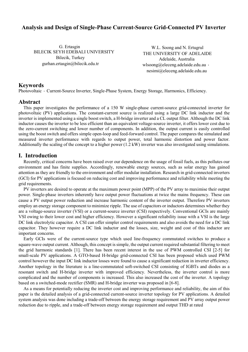
The proposed system consists of two stages (see Fig. 1). In the first stage, the PV array is connected to a circuit
resembling a boost converter, which has a sufficiently large input inductor to make the PV current relatively constant
over a fundamental (50Hz) cycle. The combination of the PV array and input inductor acts as a constant- current
source. The boost switch in this circuit acts as a current waveshaper (WS) and is used to produce a pulse- width
modulated (PWM) output current, whose fundamental component is a full-wave rectified sinewave that is
synchronized with the grid voltage. The second stage of the converter consists of a line-frequency commutated
H-bridge with thyristors which unfolds (reverses the polarity of) the sinewave current to produce an AC output
current. A low-pass line filter (CL) is utilised to remove the high-frequency PWM components to produce a
sinusoidal output current.
B. Analysis of PV Array Output Power Reduction Due to Ripple
Fig. 1: Proposed current-source inverter topology for the grid-connected
PV system with idealised current waveforms.
t
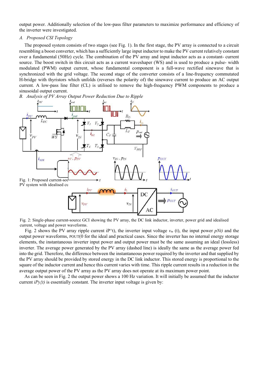
Fig. 2: Single-phase current-source GCI showing the PV array, the DC link inductor, inverter, power grid and idealised
current, voltage and power waveforms.
Fig. 2 shows the PV array ripple current iP^t), the inverter input voltage vm (t), the input power pNt) and the
output power waveforms, POUT(0 for the ideal and practical cases. Since the inverter has no internal energy storage
elements, the instantaneous inverter input power and output power must be the same assuming an ideal (lossless)
inverter. The average power generated by the PV array (dashed line) is ideally the same as the average power fed
into the grid. Therefore, the difference between the instantaneous power required by the inverter and that supplied by
the PV array should be provided by stored energy in the DC link inductor. This stored energy is proportional to the
square of the inductor current and hence this current varies with time. This ripple current results in a reduction in the
average output power of the PV array as the PV array does not operate at its maximum power point.
As can be seen in Fig. 2 the output power shows a 100 Hz variation. It will initially be assumed that the inductor
current iPy{t) is essentially constant. The inverter input voltage is given by:
�
As the inductor acts as a short circuit to DC, it can also be assumed that vPV is constant and has a value that is equal
to the average value of vv(X). If it is initially assumed that both ipv(t) and Vpv are constant then the output power of
the PV array is constant though the instantaneous input power of the inverter is time-varying. This implies the DC
link inductor must provide the required energy storage by absorbing or releasing the difference in power between
what the PV array provides and what the inverter requires.
It can be shown that there is a simple relationship between the PV array current or voltage ripple in
current and voltage source inverters, and the output power and the amount of stored energy required
E0 (2-3) [9].
Ai _ AE _ P0 /。_ 2E0 _ 減。
A similar calculation can be performed for PV VSI inverters with a large DC link capacitor to obtain:
Av _ AE _ PQ
V0
2E0
2 減 0
(2)
(3)
where Po is the average inverter output power, 0) is the angular frequency of the grid voltage, AI is the
current ripple, AV is the voltage ripple and AE is the peak energy variation.
C. Trade-off in PV Power Reduction due to Ripple versus Energy Storage Element Losses
The amount of energy storage will be measured using the ratio of the energy E stored in the inductor to the rated
PV panel output power and is given in millijoule per watt (mJ/W). Ripple in the PV panel voltage or current causes
the PV panel not to operate at its maximum power point and hence results in an average power reduction.
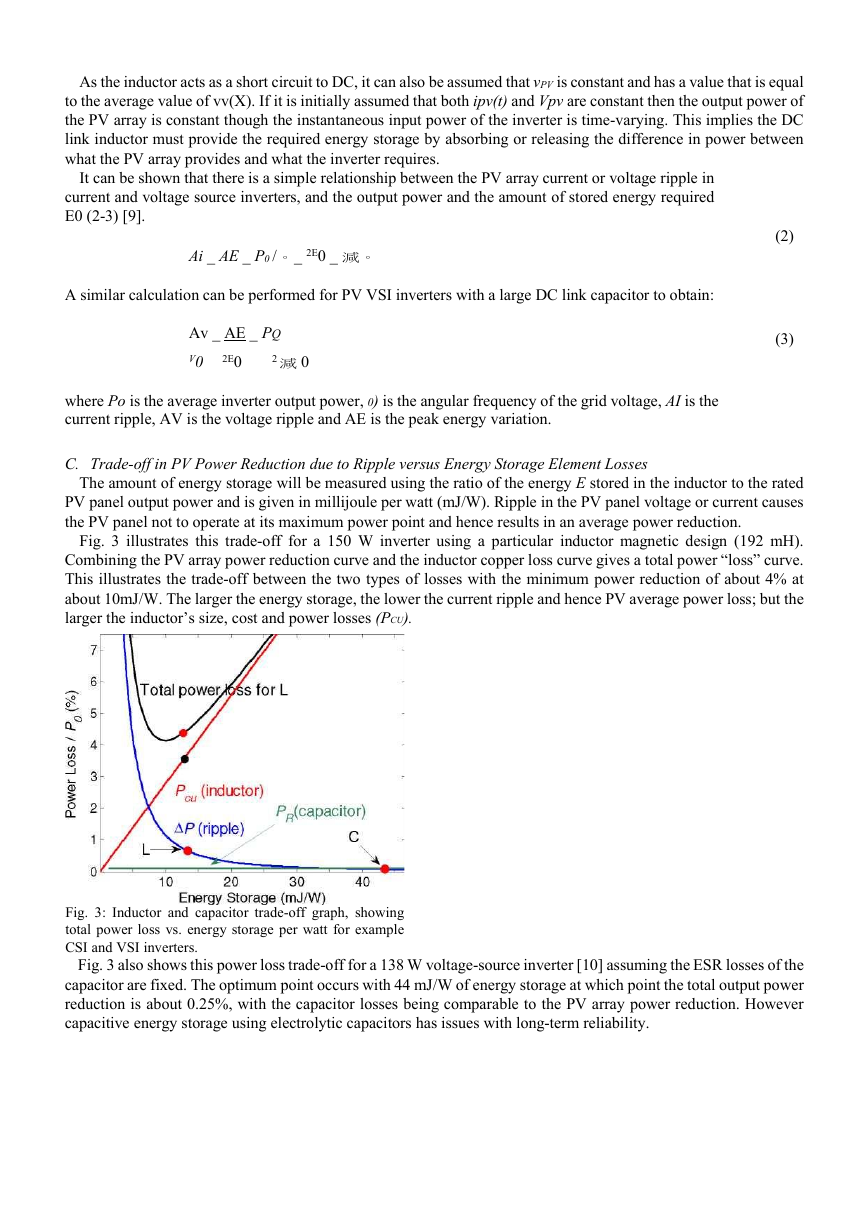
Fig. 3 illustrates this trade-off for a 150 W inverter using a particular inductor magnetic design (192 mH).
Combining the PV array power reduction curve and the inductor copper loss curve gives a total power “loss” curve.
This illustrates the trade-off between the two types of losses with the minimum power reduction of about 4% at
about 10mJ/W. The larger the energy storage, the lower the current ripple and hence PV average power loss; but the
larger the inductor’s size, cost and power losses (PCU).
Fig. 3: Inductor and capacitor trade-off graph, showing
total power loss vs. energy storage per watt for example
CSI and VSI inverters.
Fig. 3 also shows this power loss trade-off for a 138 W voltage-source inverter [10] assuming the ESR losses of the
capacitor are fixed. The optimum point occurs with 44 mJ/W of energy storage at which point the total output power
reduction is about 0.25%, with the capacitor losses being comparable to the PV array power reduction. However
capacitive energy storage using electrolytic capacitors has issues with long-term reliability.
�
D. Effect of Energy Storage on Grid Current THD
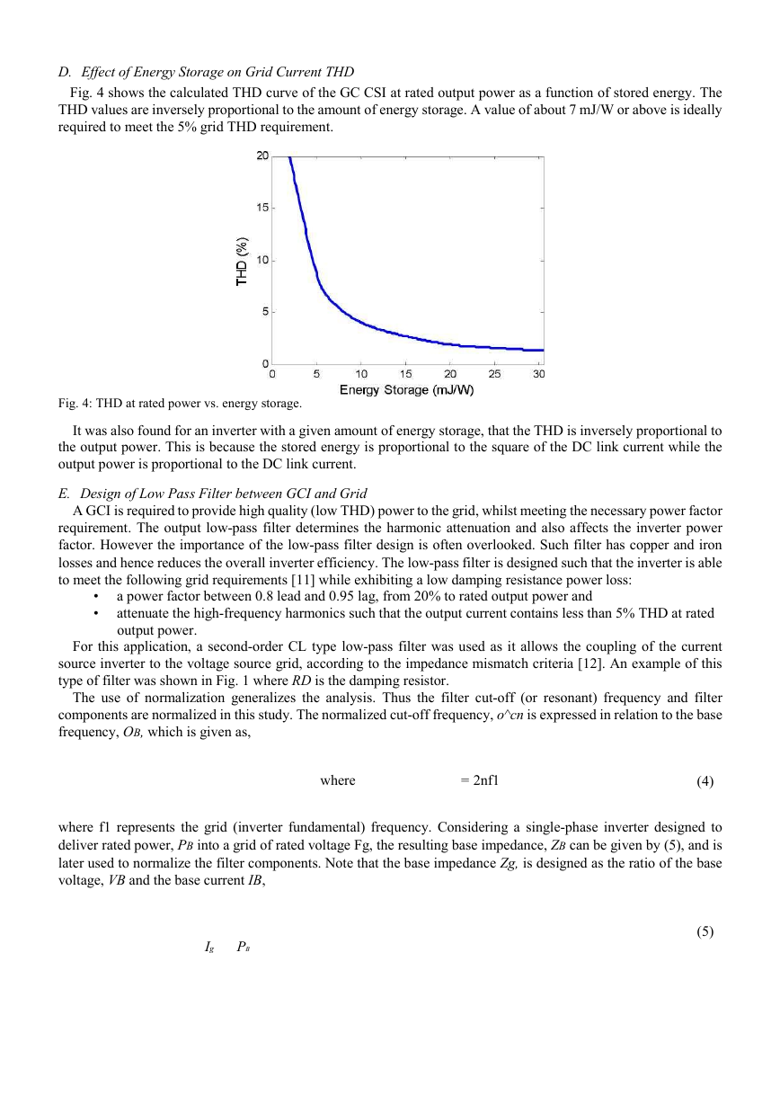
Fig. 4 shows the calculated THD curve of the GC CSI at rated output power as a function of stored energy. The
THD values are inversely proportional to the amount of energy storage. A value of about 7 mJ/W or above is ideally
required to meet the 5% grid THD requirement.
Fig. 4: THD at rated power vs. energy storage.
It was also found for an inverter with a given amount of energy storage, that the THD is inversely proportional to
the output power. This is because the stored energy is proportional to the square of the DC link current while the
output power is proportional to the DC link current.
E. Design of Low Pass Filter between GCI and Grid
A GCI is required to provide high quality (low THD) power to the grid, whilst meeting the necessary power factor
requirement. The output low-pass filter determines the harmonic attenuation and also affects the inverter power
factor. However the importance of the low-pass filter design is often overlooked. Such filter has copper and iron
losses and hence reduces the overall inverter efficiency. The low-pass filter is designed such that the inverter is able
to meet the following grid requirements [11] while exhibiting a low damping resistance power loss:
•
•
a power factor between 0.8 lead and 0.95 lag, from 20% to rated output power and
attenuate the high-frequency harmonics such that the output current contains less than 5% THD at rated
output power.
For this application, a second-order CL type low-pass filter was used as it allows the coupling of the current
source inverter to the voltage source grid, according to the impedance mismatch criteria [12]. An example of this
type of filter was shown in Fig. 1 where RD is the damping resistor.
The use of normalization generalizes the analysis. Thus the filter cut-off (or resonant) frequency and filter
components are normalized in this study. The normalized cut-off frequency, o^cn is expressed in relation to the base
frequency, OB, which is given as,
where
= 2nf1
(4)
where f1 represents the grid (inverter fundamental) frequency. Considering a single-phase inverter designed to
deliver rated power, PB into a grid of rated voltage Fg, the resulting base impedance, ZB can be given by (5), and is
later used to normalize the filter components. Note that the base impedance Zg, is designed as the ratio of the base
voltage, VB and the base current IB,
Ig
PB
(5)
�
The normalized filter capacitance, Cn is given in (6), where CB is the base capacitance. Similarly, the normalized
filter inductance, Ln is expressed relative to the base inductance, LB [13].
A baseline filter design is determined as follows. The normalized capacitance Cn is selected as 0.1 pu to meet the
where
CB-- 1
①BZB
where
LB =
(6)
C
CB
L
L
L n
leading power factor requirements. The cut-off frequency fc is chosen as 500 Hz which is an order of magnitude
above the fundamental frequency to prevent significant filter phase delay and roughly an order of magnitude below
the selected switching frequency (4 kHz). Based on the recommendation [12] regarding a quality factor of Q of 2 to
4, a value of 4 was selected. Note that Q is dependent on the filter topology and the type of damping used.
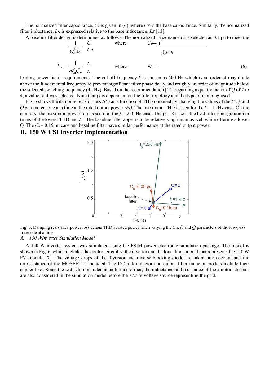
Fig. 5 shows the damping resistor loss (Pd) as a function of THD obtained by changing the values of the Cn, fcand
Q parameters one at a time at the rated output power (Po). The maximum THD is seen for the fc = 1 kHz case. On the
contrary, the maximum power loss is seen for the fc = 250 Hz case. The Q = 8 case is the best filter configuration in
terms of the lowest THD and Pd. The baseline filter appears to be relatively optimum as well while offering a lower
Q. The Cn = 0.15 pu case and baseline filter have similar performance at the rated output power.
II. 150 W CSI Inverter Implementation
2.5
2
1.5
1
0.5
0 1
2
3
THD (%)
4
5
6
Fig. 5: Damping resistance power loss versus THD at rated power when varying the Cn, fc and Q parameters of the low-pass
filter one at a time.
A. 150 WInverter Simulation Model
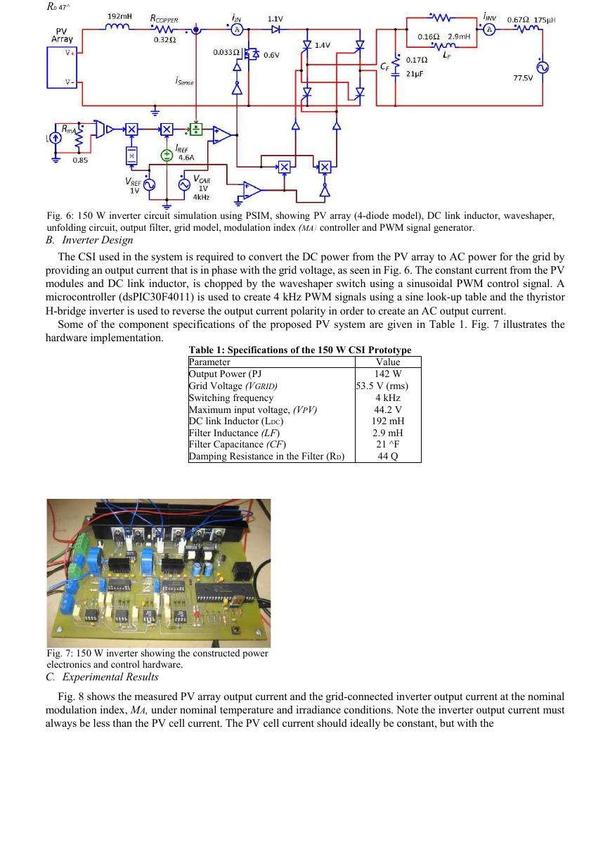
A 150 W inverter system was simulated using the PSIM power electronic simulation package. The model is
shown in Fig. 6, which includes the control circuitry, the inverter and the four-diode model that represents the 150 W
PV module [7]. The voltage drops of the thyristor and reverse-blocking diode are taken into account and the
on-resistance of the MOSFET is included. The DC link inductor and output filter inductor models include their
copper loss. Since the test setup included an autotransformer, the inductance and resistance of the autotransformer
are also considered in the simulation model before the 77.5 V voltage source representing the grid.
�
RD 47^
Fig. 6: 150 W inverter circuit simulation using PSIM, showing PV array (4-diode model), DC link inductor, waveshaper,
unfolding circuit, output filter, grid model, modulation index (MA) controller and PWM signal generator.
B. Inverter Design
The CSI used in the system is required to convert the DC power from the PV array to AC power for the grid by
providing an output current that is in phase with the grid voltage, as seen in Fig. 6. The constant current from the PV
modules and DC link inductor, is chopped by the waveshaper switch using a sinusoidal PWM control signal. A
microcontroller (dsPIC30F4011) is used to create 4 kHz PWM signals using a sine look-up table and the thyristor
H-bridge inverter is used to reverse the output current polarity in order to create an AC output current.
Some of the component specifications of the proposed PV system are given in Table 1. Fig. 7 illustrates the
hardware implementation.
Value
142 W
53.5 V (rms)
Table 1: Specifications of the 150 W CSI Prototype
Parameter
Output Power (PJ
Grid Voltage (VGRID)
Switching frequency
Maximum input voltage, (VPV)
DC link Inductor (LDC)
Filter Inductance (LF)
Filter Capacitance (CF)
Damping Resistance in the Filter (RD)
4 kHz
44.2 V
192 mH
2.9 mH
21 ^F
44 Q
Fig. 7: 150 W inverter showing the constructed power
electronics and control hardware.
C. Experimental Results
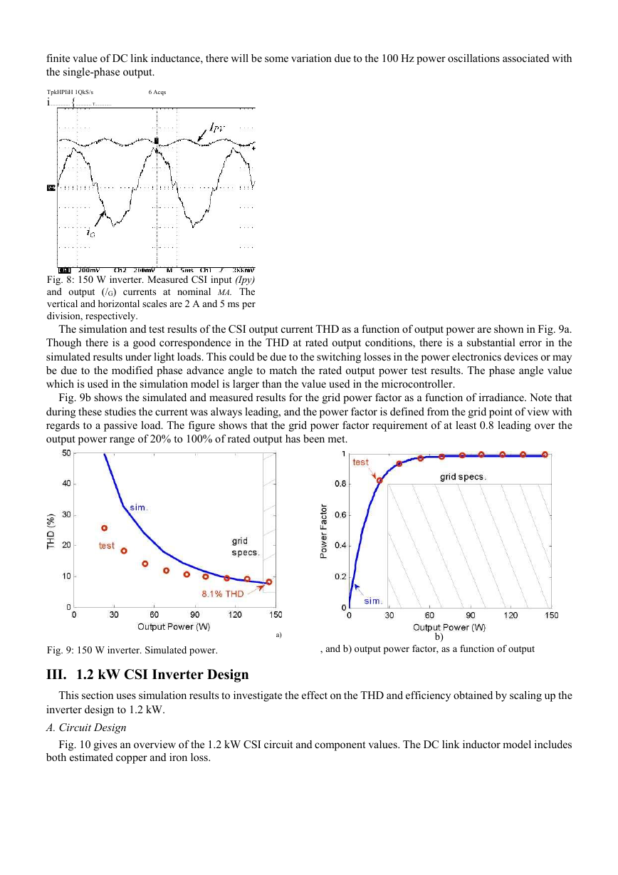
Fig. 8 shows the measured PV array output current and the grid-connected inverter output current at the nominal
modulation index, MA, under nominal temperature and irradiance conditions. Note the inverter output current must
always be less than the PV cell current. The PV cell current should ideally be constant, but with the
�
finite value of DC link inductance, there will be some variation due to the 100 Hz power oscillations associated with
the single-phase output.
TpkHPIiH 1QkS/s
i....................{................ T................
6 Acqs
Fig. 8: 150 W inverter. Measured CSI input (Ipy)
and output (/G) currents at nominal MA. The
vertical and horizontal scales are 2 A and 5 ms per
division, respectively.
The simulation and test results of the CSI output current THD as a function of output power are shown in Fig. 9a.
Though there is a good correspondence in the THD at rated output conditions, there is a substantial error in the
simulated results under light loads. This could be due to the switching losses in the power electronics devices or may
be due to the modified phase advance angle to match the rated output power test results. The phase angle value
which is used in the simulation model is larger than the value used in the microcontroller.
Fig. 9b shows the simulated and measured results for the grid power factor as a function of irradiance. Note that
during these studies the current was always leading, and the power factor is defined from the grid point of view with
regards to a passive load. The figure shows that the grid power factor requirement of at least 0.8 leading over the
output power range of 20% to 100% of rated output has been met.
Fig. 9: 150 W inverter. Simulated power.
III. 1.2 kW CSI Inverter Design
a)
, and b) output power factor, as a function of output
b)
This section uses simulation results to investigate the effect on the THD and efficiency obtained by scaling up the
inverter design to 1.2 kW.
A. Circuit Design
Fig. 10 gives an overview of the 1.2 kW CSI circuit and component values. The DC link inductor model includes
both estimated copper and iron loss.
�
Fig. 10: 1.2 kW inverter. PSIM simulation model including feed-forward control.
LDC
RD issa
The inductor was designed for the 1.2 kW inverter by linearly scaling the inductor design used for the 150 W
inverter [9]. An energy storage value of 12 mJ/W was chosen which gave a stored energy of about 15 J.
The inverter output THD was 4.3% under open-loop control and 2.8% for the feed-forward control (FFD) mode.
The FFD control uses the measured instantaneous DC link current to compensate for the 100 Hz ripple effect and so
reduces this distortion.
The low-pass line filter for the 1.2 kW inverter was designed using the same approach described in section I.E.
Although a 4 kHz switching frequency was used, the same as the prototype unit, this could be increased to 10 or 15
kHz. The maximum value of normalized capacitance Cn of 0.12 pu was chosen that still met the leading power factor
requirement of 0.95. A value of quality factor of 4 was chosen which is within the recommended range of 2 to 4.
Finally a ratio of cut-off frequency to switching frequency of slightly over 0.15 was chosen using [13], which is a
trade-off between the grid filter loss and the THD. This resulted in a
cut-off frequency of around 620 Hz. Based on these selected values,
the filter inductance, capacitance and resistance can be calculated as
8.9 mH, 7 邻 F and 135D.
B. Calculated Losses
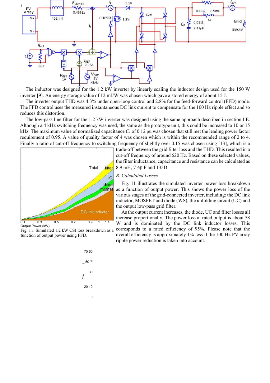
Fig. 11 illustrates the simulated inverter power loss breakdown
as a function of output power. This shows the power loss of the
various stages of the grid-connected inverter, including: the DC link
inductor, MOSFET and diode (WS), the unfolding circuit (UC) and
the output low-pass grid filter.
As the output current increases, the diode, UC and filter losses all
increase proportionally. The power loss at rated output is about 58
W and is dominated by the DC link inductor
losses. This
corresponds to a rated efficiency of 95%. Please note that the
overall efficiency is approximately 1% less if the 100 Hz PV array
ripple power reduction is taken into account.
0.5
0.3
0.1
Output Power (kW)
Fig. 11: Simulated 1.2 kW CSI loss breakdown as a
function of output power using FFD.
0.7
0.9
1
1.1
70 60
_ 50 40
30
5o
20 10
0
�


 2023年江西萍乡中考道德与法治真题及答案.doc
 2012年重庆南川中考生物真题及答案.doc
 2013年江西师范大学地理学综合及文艺理论基础考研真题.doc
 2020年四川甘孜小升初语文真题及答案I卷.doc
 2020年注册岩土工程师专业基础考试真题及答案.doc
 2023-2024学年福建省厦门市九年级上学期数学月考试题及答案.doc
 2021-2022学年辽宁省沈阳市大东区九年级上学期语文期末试题及答案.doc
 2022-2023学年北京东城区初三第一学期物理期末试卷及答案.doc
 2018上半年江西教师资格初中地理学科知识与教学能力真题及答案.doc
 2012年河北国家公务员申论考试真题及答案-省级.doc
 2020-2021学年江苏省扬州市江都区邵樊片九年级上学期数学第一次质量检测试题及答案.doc
 2022下半年黑龙江教师资格证中学综合素质真题及答案.doc