LIN
Conformance Test Specification
Package for LIN 2.1
October 10th, 2008
LIN
Conformance Test Specification Package for LIN 2.1
For the LIN Specification Package
Revision 2.1 (November 24th, 2006)
October 10th, 2008
© LIN Consortium, 2008
This specification as released by the LIN Consortium is intended for the purpose of
information only and is provided on an "AS IS" basis only and cannot be the basis for
any claims. The LIN Consortium will not be liable for any use of this Specification.
This Document must be regarded as strictly LIN Consortium Internal and must not be
distributed outside the LIN Consortium. The use is restricted for the assignee, his col-
leagues, and employees of any affiliates of his company.
The unauthorized use, e.g. copying, displaying or other use of any content from this
document is a violation of the law and intellectual property rights.
LIN is a registered Trademark ®. All rights reserved.
All distributions are registered.
Website: www.lin-subbus.org Contact: info@lin-subbus.org
i
m
o
c
.
c
m
e
t
@
s
u
a
s
e
i
l
.
k
n
a
r
f
r
o
f
y
p
o
c
d
e
r
e
t
s
g
e
R
i
�
LIN
Conformance Test Specification
Package for LIN 2.1
October 10th, 2008
i
m
o
c
.
c
m
e
t
@
s
u
a
s
e
i
l
.
k
n
a
r
f
r
o
f
y
p
o
c
d
e
r
e
t
s
g
e
R
i
Website: www.lin-subbus.org Contact: info@lin-subbus.org
�
LIN
Conformance Test Specification
OSI Layer 1 – Physical Layer
Version 2.1
October 10th, 2008; Page 1
LIN
Conformance Test Specification
LIN OSI Layer 1 – Physical Layer
For LIN devices with Rx and Tx access
For the LIN Physical Layer Specification
Revision 2.1 (November 24th, 2006)
Version 2.1
October 10th, 2008
i
m
o
c
.
c
m
e
t
@
s
u
a
s
e
i
l
.
k
n
a
r
f
r
o
f
y
p
o
c
d
e
r
e
t
s
g
e
R
i
Website: www.lin-subbus.org Contact: info@lin-subbus.org
�
Table of Contents
LIN
Conformance Test Specification
OSI Layer 1 – Physical Layer
Version 2.1
October 10th, 2008; Page 2
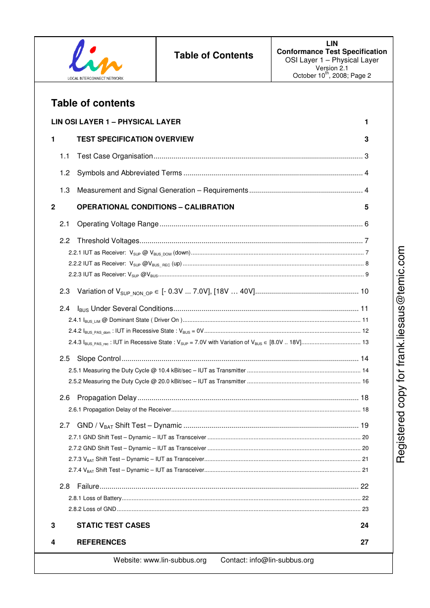
Table of contents
LIN OSI LAYER 1 – PHYSICAL LAYER
TEST SPECIFICATION OVERVIEW
1
3
1.1 Test Case Organisation......................................................................................................... 3
1.2 Symbols and Abbreviated Terms .......................................................................................... 4
1.3 Measurement and Signal Generation – Requirements ......................................................... 4
OPERATIONAL CONDITIONS – CALIBRATION
5
2.1 Operating Voltage Range ...................................................................................................... 6
2.2 Threshold Voltages................................................................................................................ 7
2.2.1 IUT as Receiver: VSUP @ VBUS_DOM (down)......................................................................................................... 7
2.2.2 IUT as Receiver: VSUP @VBUS_ REC (up) .............................................................................................................. 8
2.2.3 IUT as Receiver: VSUP @VBUS............................................................................................................................. 9
2.3 Variation of VSUP_NON_OP ∈ [- 0.3V ... 7.0V], [18V … 40V].................................................... 10
2.4
IBUS Under Several Conditions............................................................................................. 11
2.4.1 IBUS_LIM @ Dominant State ( Driver On )............................................................................................................ 11
2.4.2 IBUS_PAS_dom : IUT in Recessive State : VBUS = 0V............................................................................................... 12
2.4.3 IBUS_PAS_rec : IUT in Recessive State : VSUP = 7.0V with Variation of VBUS ∈ [8.0V .. 18V].................................... 13
2.5 Slope Control....................................................................................................................... 14
2.5.1 Measuring the Duty Cycle @ 10.4 kBit/sec – IUT as Transmitter ..................................................................... 14
2.5.2 Measuring the Duty Cycle @ 20.0 kBit/sec – IUT as Transmitter ..................................................................... 16
2.6 Propagation Delay ............................................................................................................... 18
2.6.1 Propagation Delay of the Receiver................................................................................................................... 18
2.7 GND / VBAT Shift Test – Dynamic ........................................................................................ 19
2.7.1 GND Shift Test – Dynamic – IUT as Transceiver ............................................................................................. 20
2.7.2 GND Shift Test – Dynamic – IUT as Transceiver ............................................................................................. 20
2.7.3 VBAT Shift Test – Dynamic – IUT as Transceiver............................................................................................... 21
2.7.4 VBAT Shift Test – Dynamic – IUT as Transceiver............................................................................................... 21
2.8 Failure.................................................................................................................................. 22
2.8.1 Loss of Battery................................................................................................................................................. 22
2.8.2 Loss of GND .................................................................................................................................................... 23
STATIC TEST CASES
REFERENCES
24
27
Website: www.lin-subbus.org Contact: info@lin-subbus.org
i
m
o
c
.
c
m
e
t
@
s
u
a
s
e
i
l
.
k
n
a
r
f
r
o
f
y
p
o
c
d
e
r
e
t
s
g
e
R
i
1
2
3
4
�
Test Specification
overview
LIN
Conformance Test Specification
OSI Layer 1 – Physical Layer
Version 2.1
October 10th, 2008; Page 3
1
Test Specification overview
1.1 Test Case Organisation
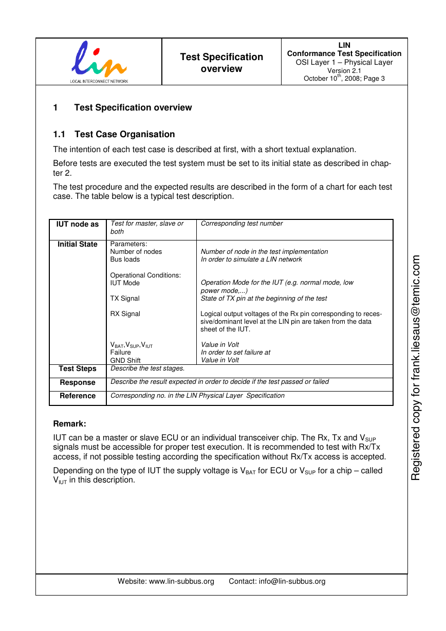
The intention of each test case is described at first, with a short textual explanation.
Before tests are executed the test system must be set to its initial state as described in chap-
ter 2.
The test procedure and the expected results are described in the form of a chart for each test
case. The table below is a typical test description.
IUT node as
Test for master, slave or
both
Corresponding test number
Initial State
Test Steps
Parameters:
Number of nodes
Bus loads
Operational Conditions:
IUT Mode
TX Signal
RX Signal
VBAT,VSUP,VIUT
Failure
GND Shift
Describe the test stages.
Number of node in the test implementation
In order to simulate a LIN network
Operation Mode for the IUT (e.g. normal mode, low
power mode,...)
State of TX pin at the beginning of the test
Logical output voltages of the Rx pin corresponding to reces-
sive/dominant level at the LIN pin are taken from the data
sheet of the IUT.
Value in Volt
In order to set failure at
Value in Volt
Response
Describe the result expected in order to decide if the test passed or failed
Reference
Corresponding no. in the LIN Physical Layer Specification
Remark:
IUT can be a master or slave ECU or an individual transceiver chip. The Rx, Tx and VSUP
signals must be accessible for proper test execution. It is recommended to test with Rx/Tx
access, if not possible testing according the specification without Rx/Tx access is accepted.
Depending on the type of IUT the supply voltage is VBAT for ECU or VSUP for a chip – called
VIUT in this description.
i
m
o
c
.
c
m
e
t
@
s
u
a
s
e
i
l
.
k
n
a
r
f
r
o
f
y
p
o
c
d
e
r
e
t
s
g
e
R
i
Website: www.lin-subbus.org Contact: info@lin-subbus.org
�
Test Specification
overview
LIN
Conformance Test Specification
OSI Layer 1 – Physical Layer
Version 2.1
October 10th, 2008; Page 4
1.2 Symbols and Abbreviated Terms
IUT
Implementation under Test
Tx
Rx
TRX
VBAT
VSUP
VIUT
VBUS
Tx pin of the transceiver
Rx pin of the transceiver
Transceiver
Voltage at ECU supply pins
Voltage at transceiver supply pins
Voltage at IUT supply pins
Voltage on the LIN bus
LIN Bus
LIN network
GND
Ground
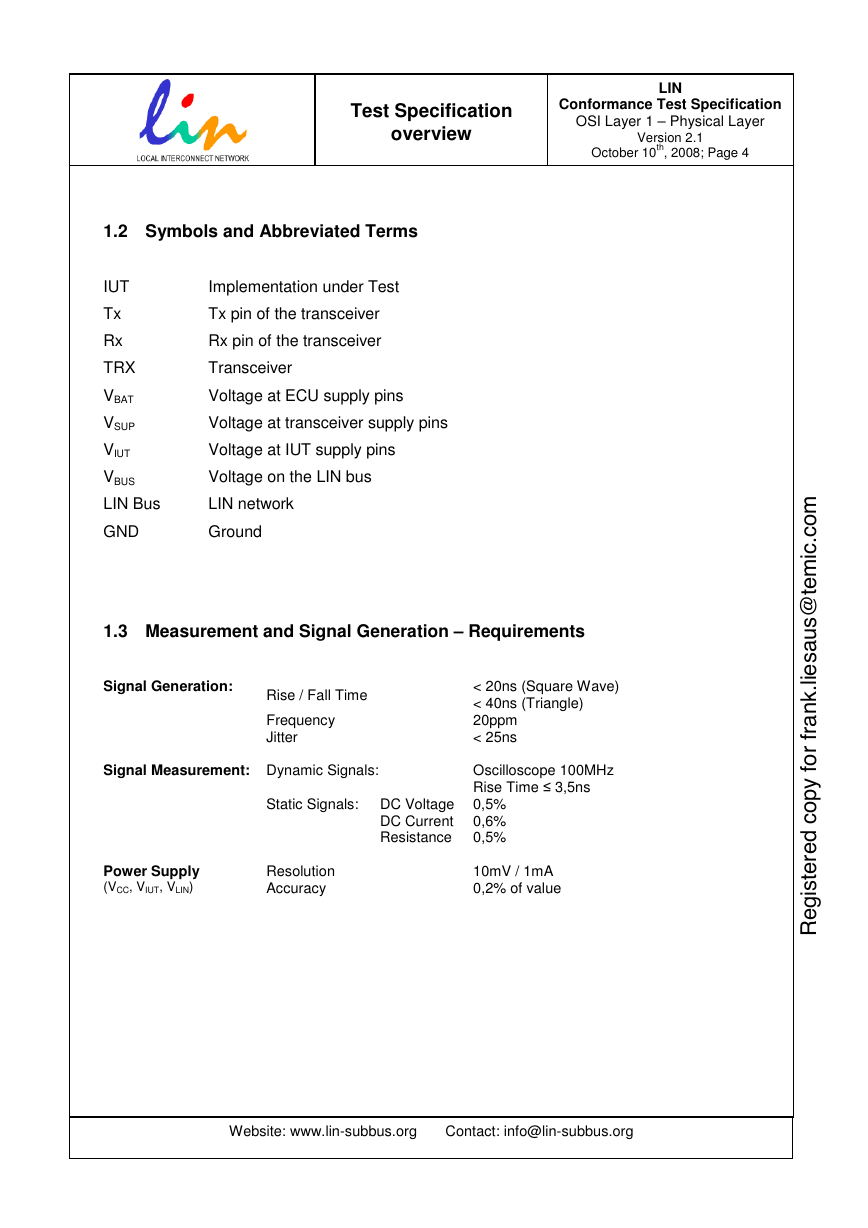
1.3 Measurement and Signal Generation – Requirements
Signal Generation:
Rise / Fall Time
Signal Measurement: Dynamic Signals:
Frequency
Jitter
< 20ns (Square Wave)
< 40ns (Triangle)
20ppm
< 25ns
Oscilloscope 100MHz
Rise Time ≤ 3,5ns
Power Supply
(VCC, VIUT, VLIN)
Static Signals: DC Voltage 0,5%
DC Current 0,6%
0,5%
Resistance
10mV / 1mA
Resolution
0,2% of value
Accuracy
Website: www.lin-subbus.org Contact: info@lin-subbus.org
i
m
o
c
.
c
m
e
t
@
s
u
a
s
e
i
l
.
k
n
a
r
f
r
o
f
y
p
o
c
d
e
r
e
t
s
g
e
R
i
�
Operational Conditions
– Calibration
LIN
Conformance Test Specification
OSI Layer 1 – Physical Layer
Version 2.1
October 10th, 2008; Page 5
2 Operational Conditions – Calibration
(Electrical input/output, LIN Protocol)
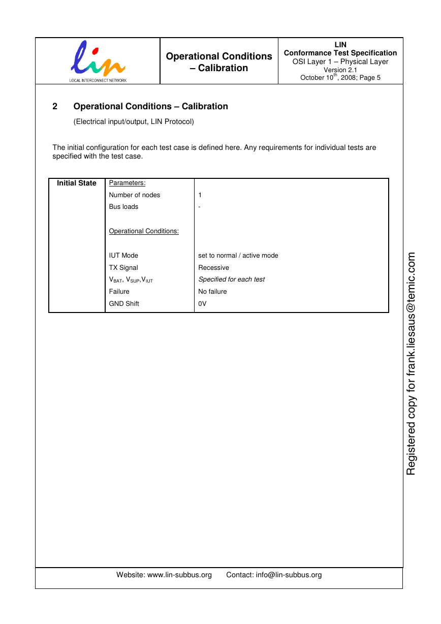
The initial configuration for each test case is defined here. Any requirements for individual tests are
specified with the test case.
Initial State
Parameters:
Number of nodes
Bus loads
Operational Conditions:
IUT Mode
TX Signal
1
-
set to normal / active mode
Recessive
VBAT, VSUP,VIUT
Specified for each test
Failure
GND Shift
No failure
0V
i
m
o
c
.
c
m
e
t
@
s
u
a
s
e
i
l
.
k
n
a
r
f
r
o
f
y
p
o
c
d
e
r
e
t
s
g
e
R
i
Website: www.lin-subbus.org Contact: info@lin-subbus.org
�
Operational Conditions
– Calibration
LIN
Conformance Test Specification
OSI Layer 1 – Physical Layer
Version 2.1
October 10th, 2008; Page 6
2.1 Operating Voltage Range
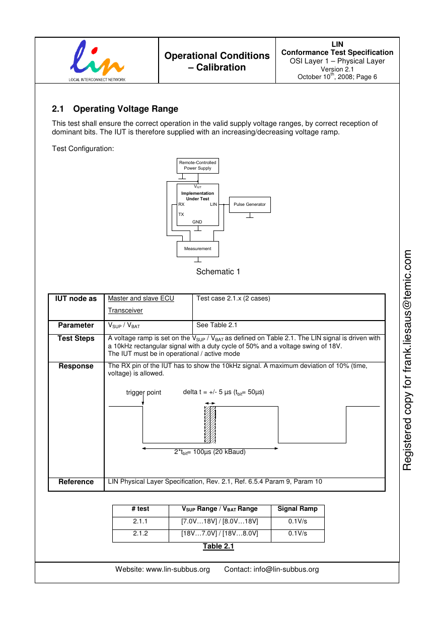
This test shall ensure the correct operation in the valid supply voltage ranges, by correct reception of
dominant bits. The IUT is therefore supplied with an increasing/decreasing voltage ramp.
Test Configuration:
Remote-Controlled
Power Supply
VIUT
Implementation
Under Test
LIN
Pulse Generator
RX
TX
GND
Measurement
Schematic 1
IUT node as
Master and slave ECU
Test case 2.1.x (2 cases)
Transceiver
Parameter
VSUP / VBAT
See Table 2.1
Test Steps
A voltage ramp is set on the VSUP / VBAT as defined on Table 2.1. The LIN signal is driven with
a 10kHz rectangular signal with a duty cycle of 50% and a voltage swing of 18V.
The IUT must be in operational / active mode
Response
The RX pin of the IUT has to show the 10kHz signal. A maximum deviation of 10% (time,
voltage) is allowed.
trigger point
delta t = +/ - 5 µs ( t bit = 50 µs )
2 * t bit = 100 µs ( 20 kBaud )
Reference
LIN Physical Layer Specification, Rev. 2.1, Ref. 6.5.4 Param 9, Param 10
# test
2.1.1
2.1.2
VSUP Range / VBAT Range
Signal Ramp
[7.0V…18V] / [8.0V…18V]
[18V…7.0V] / [18V…8.0V]
0.1V/s
0.1V/s
Table 2.1
Website: www.lin-subbus.org Contact: info@lin-subbus.org
i
m
o
c
.
c
m
e
t
@
s
u
a
s
e
i
l
.
k
n
a
r
f
r
o
f
y
p
o
c
d
e
r
e
t
s
g
e
R
i
�


 2023年江西萍乡中考道德与法治真题及答案.doc
 2012年重庆南川中考生物真题及答案.doc
 2013年江西师范大学地理学综合及文艺理论基础考研真题.doc
 2020年四川甘孜小升初语文真题及答案I卷.doc
 2020年注册岩土工程师专业基础考试真题及答案.doc
 2023-2024学年福建省厦门市九年级上学期数学月考试题及答案.doc
 2021-2022学年辽宁省沈阳市大东区九年级上学期语文期末试题及答案.doc
 2022-2023学年北京东城区初三第一学期物理期末试卷及答案.doc
 2018上半年江西教师资格初中地理学科知识与教学能力真题及答案.doc
 2012年河北国家公务员申论考试真题及答案-省级.doc
 2020-2021学年江苏省扬州市江都区邵樊片九年级上学期数学第一次质量检测试题及答案.doc
 2022下半年黑龙江教师资格证中学综合素质真题及答案.doc