ESD in Silicon Integrated Circuits, 2nd Edition
Ajith Amerasekera, Charvaka Duvvury
Copyright c 2002 John Wiley & Sons, Ltd
ISB N s : 0-471-49871-8 (Hardback); 0-470-84605-4 (Electronic)
ESD in Silicon
Integrated Circuits
Second Edition
�
ESD in Silicon
Integrated Circuits
Second Edition
Ajith Amerasekera
Charvaka Duvvury
Texas Instruments, Inc., USA
With
Warren Anderson
Compaq Computer Corporation, USA
Horst Gieser
Fraunhofer Institute for Reliability and
Microintegration IZM ATIS, Germany
Sridhar Ramaswamy
Texas Instruments, Inc., USA
�
Copyright c 2002 by John Wiley & Sons, Ltd.,
Baffins Lane, Chichester,
West Sussex PO 19 1UD, England
Phone (+44) 1243 779777
e-mail (for orders and customer service enquiries): cs-books@wiley.co.uk
Visit our Home Page on http://www.wileyeurope.com or http://www.wiley.com
All Rights Reserved. No part of this publication may be reproduced, stored in a retrieval system or
transmitted in any form or by any means, electronic, mechanical, photocopying, recording, scanning
or otherwise, except under the terms of the Copyright, Designs and Patents Act 1988 or under the
terms of a license issued by the Copyright Licensing Agency Ltd., 90 Tottenham Court Road, London
W1P 0LP, UK without the permission in writing of the Publisher. Requests to the Publisher should be
addressed to the Permissions Department, John Wiley & Sons, Ltd., Baffins Lane, Chichester, West
Sussex PO 19 1UD, England, or emailed to permreq@wiley.co.uk, or faxed to (+44) 1243 770571.
Other Wiley Editorial Offices
John Wiley & Sons, Inc., 605 Third Avenue,
New York, NY 10158-0012, USA
Jossey-Bass, 989 Market Street,
San Francisco, CA 94103-1741, USA
WILEY-VCH Verlag GmbH, Pappelallee 3,
D-69469 Weinheim, Germany
John Wiley & Sons Australia, Ltd., 33 Park Road,
Milton, Queensland 4064, Australia
John Wiley & Sons (Asia) Pte Ltd., 2 Clementi Loop #02-01,
Jin Xing Distripark, Singapore 129809
John Wiley & Sons Canada, Ltd., 22 Worcester Road,
Etobicoke, Ontario, Canada M9W 1L1
British Library Cataloguing in Publication Data
A catalogue record for this book is available from the British Library
ISBN 0 470 49871 8
Typeset in 10/12pt Times by Laserwords Private Limited, Chennai, India.
Printed and bound in Great Britain by Antony Rowe Ltd., Chippenham, Wiltshire.
This book is printed on acid-free paper responsibly manufactured from sustainable forestry
in which at least two trees are planted for each one used for paper production.
�
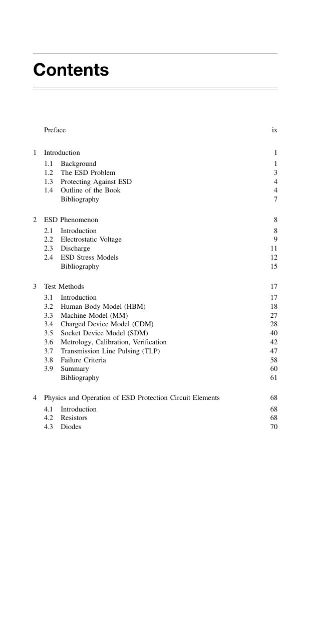
Contents
Preface
1 Introduction
1.1 Background
1.2 The ESD Problem
1.3 Protecting Against ESD
1.4 Outline of the Book
Bibliography
2 ESD Phenomenon
Introduction
2.1
2.2 Electrostatic Voltage
2.3 Discharge
2.4 ESD Stress Models
Bibliography
3 Test Methods
Introduction
3.1
3.2 Human Body Model (HBM)
3.3 Machine Model (MM)
3.4 Charged Device Model (CDM)
3.5 Socket Device Model (SDM)
3.6 Metrology, Calibration, Verification
3.7 Transmission Line Pulsing (TLP)
3.8 Failure Criteria
3.9 Summary
Bibliography
4 Physics and Operation of ESD Protection Circuit Elements
Introduction
4.1
4.2 Resistors
4.3 Diodes
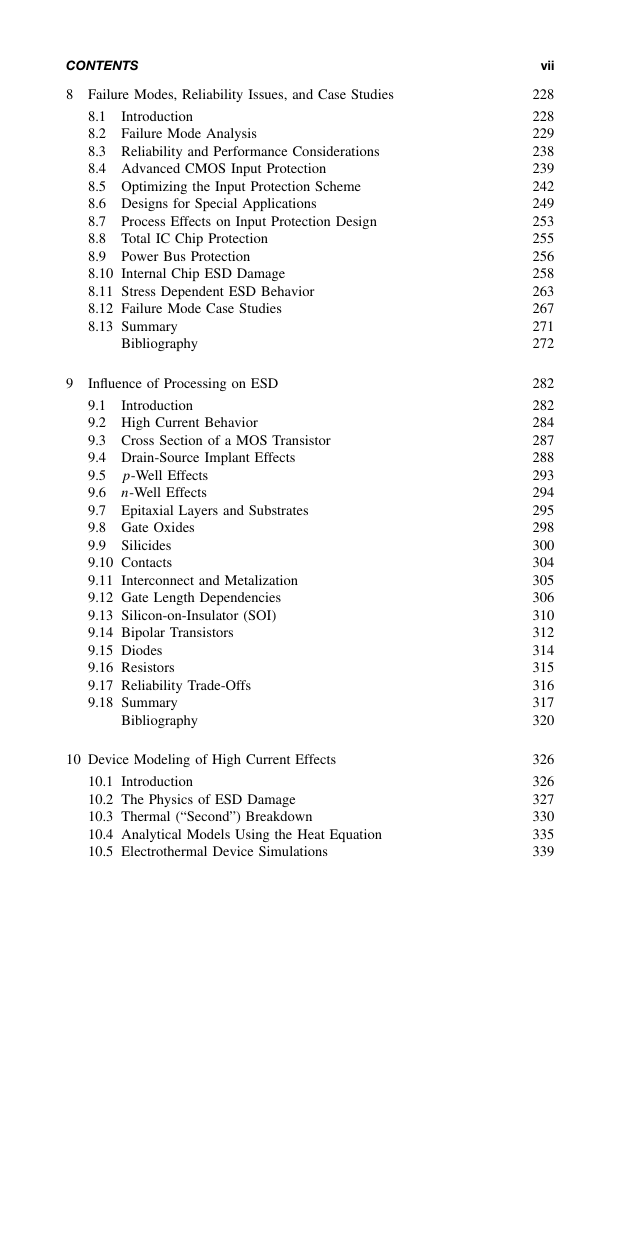
ix
1
1
3
4
4
7
8
8
9
11
12
15
17
17
18
27
28
40
42
47
58
60
61
68
68
68
70
�
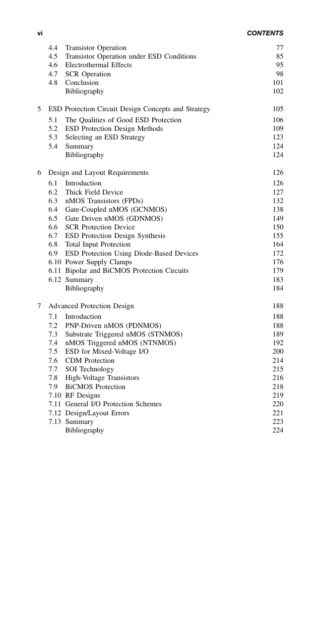
vi
CONTENTS
4.4 Transistor Operation
4.5 Transistor Operation under ESD Conditions
4.6 Electrothermal Effects
4.7 SCR Operation
4.8 Conclusion
Bibliography
5 ESD Protection Circuit Design Concepts and Strategy
5.1 The Qualities of Good ESD Protection
5.2 ESD Protection Design Methods
5.3 Selecting an ESD Strategy
5.4 Summary
Bibliography
6 Design and Layout Requirements
Introduction
nMOS Transistors (FPDs)
6.1
6.2 Thick Field Device
6.3
6.4 Gate-Coupled nMOS (GCNMOS)
6.5 Gate Driven nMOS (GDNMOS)
6.6 SCR Protection Device
6.7 ESD Protection Design Synthesis
6.8 Total Input Protection
6.9 ESD Protection Using Diode-Based Devices
6.10 Power Supply Clamps
6.11 Bipolar and BiCMOS Protection Circuits
6.12 Summary
Bibliography
7 Advanced Protection Design
Introduction
nMOS Triggered nMOS (NTNMOS)
7.1
7.2 PNP-Driven nMOS (PDNMOS)
7.3 Substrate Triggered nMOS (STNMOS)
7.4
7.5 ESD for Mixed-Voltage I/O
7.6 CDM Protection
7.7 SOI Technology
7.8 High-Voltage Transistors
7.9 BiCMOS Protection
7.10 RF Designs
7.11 General I/O Protection Schemes
7.12 Design/Layout Errors
7.13 Summary
Bibliography
77
85
95
98
101
102
105
106
109
123
124
124
126
126
127
132
138
149
150
155
164
172
176
179
183
184
188
188
188
189
192
200
214
215
216
218
219
220
221
223
224
�
CONTENTS
8 Failure Modes, Reliability Issues, and Case Studies
Introduction
8.1
8.2 Failure Mode Analysis
8.3 Reliability and Performance Considerations
8.4 Advanced CMOS Input Protection
8.5 Optimizing the Input Protection Scheme
8.6 Designs for Special Applications
8.7 Process Effects on Input Protection Design
8.8 Total IC Chip Protection
8.9 Power Bus Protection
8.10 Internal Chip ESD Damage
8.11 Stress Dependent ESD Behavior
8.12 Failure Mode Case Studies
8.13 Summary
Bibliography
9 Influence of Processing on ESD
Introduction
9.1
9.2 High Current Behavior
9.3 Cross Section of a MOS Transistor
9.4 Drain-Source Implant Effects
9.5 p-Well Effects
9.6 n-Well Effects
9.7 Epitaxial Layers and Substrates
9.8 Gate Oxides
9.9 Silicides
9.10 Contacts
9.11 Interconnect and Metalization
9.12 Gate Length Dependencies
9.13 Silicon-on-Insulator (SOI)
9.14 Bipolar Transistors
9.15 Diodes
9.16 Resistors
9.17 Reliability Trade-Offs
9.18 Summary
Bibliography
10 Device Modeling of High Current Effects
10.1 Introduction
10.2 The Physics of ESD Damage
10.3 Thermal (“Second”) Breakdown
10.4 Analytical Models Using the Heat Equation
10.5 Electrothermal Device Simulations
vii
228
228
229
238
239
242
249
253
255
256
258
263
267
271
272
282
282
284
287
288
293
294
295
298
300
304
305
306
310
312
314
315
316
317
320
326
326
327
330
335
339
�
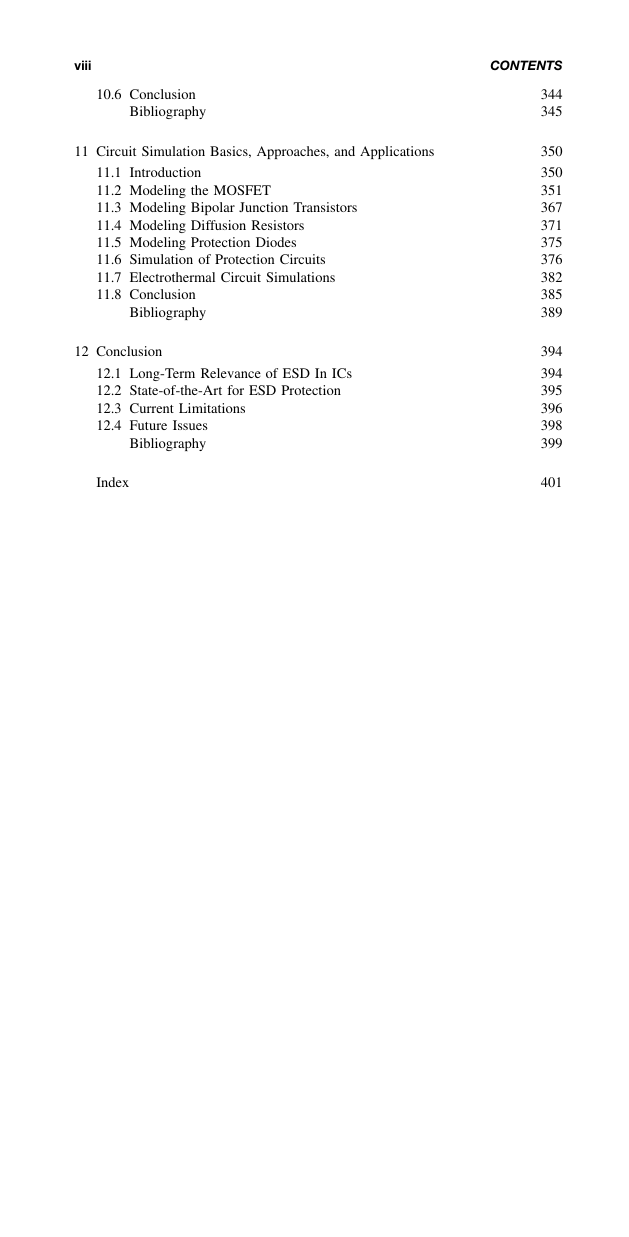
viii
10.6 Conclusion
Bibliography
11 Circuit Simulation Basics, Approaches, and Applications
11.1 Introduction
11.2 Modeling the MOSFET
11.3 Modeling Bipolar Junction Transistors
11.4 Modeling Diffusion Resistors
11.5 Modeling Protection Diodes
11.6 Simulation of Protection Circuits
11.7 Electrothermal Circuit Simulations
11.8 Conclusion
Bibliography
12 Conclusion
12.1 Long-Term Relevance of ESD In ICs
12.2 State-of-the-Art for ESD Protection
12.3 Current Limitations
12.4 Future Issues
Bibliography
Index
CONTENTS
344
345
350
350
351
367
371
375
376
382
385
389
394
394
395
396
398
399
401
�
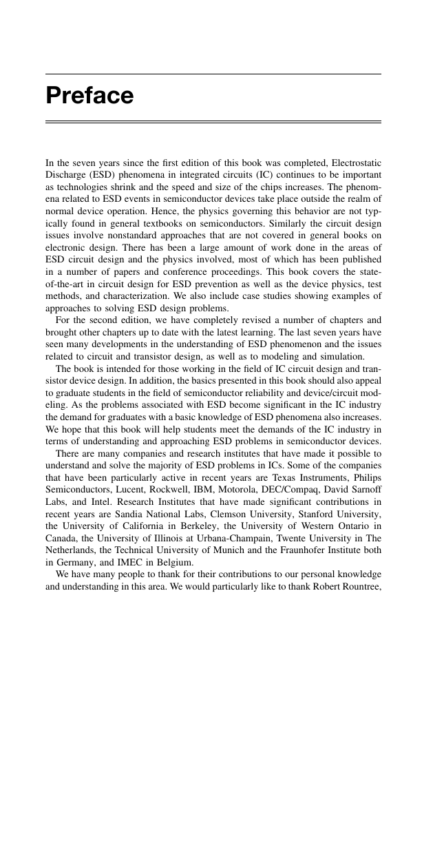
Preface
In the seven years since the first edition of this book was completed, Electrostatic
Discharge (ESD) phenomena in integrated circuits (IC) continues to be important
as technologies shrink and the speed and size of the chips increases. The phenom-
ena related to ESD events in semiconductor devices take place outside the realm of
normal device operation. Hence, the physics governing this behavior are not typ-
ically found in general textbooks on semiconductors. Similarly the circuit design
issues involve nonstandard approaches that are not covered in general books on
electronic design. There has been a large amount of work done in the areas of
ESD circuit design and the physics involved, most of which has been published
in a number of papers and conference proceedings. This book covers the state-
of-the-art in circuit design for ESD prevention as well as the device physics, test
methods, and characterization. We also include case studies showing examples of
approaches to solving ESD design problems.
For the second edition, we have completely revised a number of chapters and
brought other chapters up to date with the latest learning. The last seven years have
seen many developments in the understanding of ESD phenomenon and the issues
related to circuit and transistor design, as well as to modeling and simulation.
The book is intended for those working in the field of IC circuit design and tran-
sistor device design. In addition, the basics presented in this book should also appeal
to graduate students in the field of semiconductor reliability and device/circuit mod-
eling. As the problems associated with ESD become significant in the IC industry
the demand for graduates with a basic knowledge of ESD phenomena also increases.
We hope that this book will help students meet the demands of the IC industry in
terms of understanding and approaching ESD problems in semiconductor devices.
There are many companies and research institutes that have made it possible to
understand and solve the majority of ESD problems in ICs. Some of the companies
that have been particularly active in recent years are Texas Instruments, Philips
Semiconductors, Lucent, Rockwell, IBM, Motorola, DEC/Compaq, David Sarnoff
Labs, and Intel. Research Institutes that have made significant contributions in
recent years are Sandia National Labs, Clemson University, Stanford University,
the University of California in Berkeley, the University of Western Ontario in
Canada, the University of Illinois at Urbana-Champain, Twente University in The
Netherlands, the Technical University of Munich and the Fraunhofer Institute both
in Germany, and IMEC in Belgium.
We have many people to thank for their contributions to our personal knowledge
and understanding in this area. We would particularly like to thank Robert Rountree,
�



 2023年江西萍乡中考道德与法治真题及答案.doc
 2012年重庆南川中考生物真题及答案.doc
 2013年江西师范大学地理学综合及文艺理论基础考研真题.doc
 2020年四川甘孜小升初语文真题及答案I卷.doc
 2020年注册岩土工程师专业基础考试真题及答案.doc
 2023-2024学年福建省厦门市九年级上学期数学月考试题及答案.doc
 2021-2022学年辽宁省沈阳市大东区九年级上学期语文期末试题及答案.doc
 2022-2023学年北京东城区初三第一学期物理期末试卷及答案.doc
 2018上半年江西教师资格初中地理学科知识与教学能力真题及答案.doc
 2012年河北国家公务员申论考试真题及答案-省级.doc
 2020-2021学年江苏省扬州市江都区邵樊片九年级上学期数学第一次质量检测试题及答案.doc
 2022下半年黑龙江教师资格证中学综合素质真题及答案.doc