Kintex-7 FPGAs Data Sheet:
DC and AC Switching Characteristics
DS182 (v2.16) May 8, 2017
Product Specification
Introduction
Kintex®-7 FPGAs are available in -3, -2, -1, -1L, and -2L
speed grades, with -3 having the highest performance. The
-2L devices are screened for lower maximum static power
and can operate at lower core voltages for lower dynamic
power than the -2 devices. The -2L industrial (I) temperature
devices operate only at VCCINT = 0.95V. The -2L extended (E)
temperature devices can operate at either VCCINT = 0.9V or
1.0V. The -2LE devices when operated at VCCINT = 1.0V, and
the -2LI devices when operated at VCCINT = 0.95V, have the
same speed specifications as the -2 speed grade, except
where noted. When the -2LE devices are operated at
VCCINT = 0.9V, the speed specifications, static power, and
dynamic power are reduced. The -1L military (M)
temperature devices have the same speed specifications as
the -1 military temperature devices and are screened for
lower maximum static power.
Kintex-7 FPGA DC and AC characteristics are specified in
commercial, extended, industrial, and military temperature
ranges. Except for the operating temperature range or
unless otherwise noted, all the DC and AC electrical
parameters are the same for a particular speed grade (that
is, the timing characteristics of a -1 speed grade military
temperature device are the same as for a -1 speed grade
commercial temperature device). However, only selected
speed grades and/or devices are available in each
temperature range.
All supply voltage and junction temperature specifications
are representative of worst-case conditions. The parameters
included are common to popular designs and typical
applications.
Available device and package combinations can be found in:
•
• Defense-Grade 7 Series FPGAs Overview (DS185)
This Kintex-7 FPGA data sheet, part of an overall set of
documentation on the 7 series FPGAs, is available on the
Xilinx website at www.xilinx.com/documentation.
7 Series FPGAs Overview (DS180)
DC Characteristics
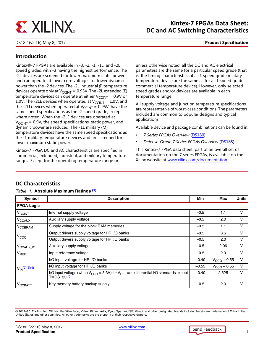
Table 1: Absolute Maximum Ratings (1)
Symbol
FPGA Logic
VCCINT
VCCAUX
VCCBRAM
VCCO
VCCAUX_IO
VREF
(2)(3)(4)
VIN
VCCBATT
Description
Min
Max
Units
Internal supply voltage
Auxiliary supply voltage
Supply voltage for the block RAM memories
Output drivers supply voltage for HR I/O banks
Output drivers supply voltage for HP I/O banks
Auxiliary supply voltage
Input reference voltage
I/O input voltage for HR I/O banks
I/O input voltage for HP I/O banks
I/O input voltage (when VCCO = 3.3V) for VREF and differential I/O standards except
TMDS_33(5)
Key memory battery backup supply
–0.5
–0.5
–0.5
–0.5
–0.5
–0.5
–0.5
–0.40
–0.55
–0.40
1.1
2.0
1.1
3.6
2.0
2.06
2.0
VCCO + 0.55
VCCO + 0.55
2.625
–0.5
2.0
V
V
V
V
V
V
V
V
V
V
V
© 2011–2017 Xilinx, Inc. XILINX, the Xilinx logo, Virtex, Kintex, Artix, Zynq, Spartan, ISE, Vivado and other designated brands included herein are trademarks of Xilinx in the
United States and other countries. All other trademarks are the property of their respective owners.
DS182 (v2.16) May 8, 2017
Product Specification
www.xilinx.com
1
Send Feedback�
Table 1: Absolute Maximum Ratings (1) (Cont’d)
Kintex-7 FPGAs Data Sheet: DC and AC Switching Characteristics
Description
Min
Max
Units
Symbol
GTX Transceiver
VMGTAVCC
VMGTAVTT
VMGTVCCAUX
VMGTREFCLK
Analog supply voltage for the GTX transmitter and receiver circuits
Analog supply voltage for the GTX transmitter and receiver termination circuits
Auxiliary analog Quad PLL (QPLL) voltage supply for the GTX transceivers
GTX transceiver reference clock absolute input voltage
VMGTAVTTRCAL
Analog supply voltage for the resistor calibration circuit of the GTX transceiver
column
Receiver (RXP/RXN) and Transmitter (TXP/TXN) absolute input voltage
DC output current for transmitter pins DC coupled RX termination = floating
DC input current for receiver input pins DC coupled RX termination = floating
DC input current for receiver input pins DC coupled RX termination = VMGTAVTT
DC input current for receiver input pins DC coupled RX termination = GND
VIN
IDCIN-FLOAT
IDCIN-MGTAVTT
IDCIN-GND
IDCOUT-FLOAT
IDCOUT-MGTAVTT DC output current for transmitter pins DC coupled RX termination = VMGTAVTT
XADC
VCCADC
VREFP
Temperature
TSTG
XADC supply relative to GNDADC
XADC reference input relative to GNDADC
Storage temperature (ambient)
Maximum soldering temperature for Pb/Sn component bodies (6)
Maximum soldering temperature for Pb-free component bodies (6)
Maximum junction temperature(6)
TSOL
Tj
–0.5
–0.5
–0.5
–0.5
–0.5
–0.5
–
–
–
–
–
–0.5
–0.5
–65
–
–
–
1.1
1.32
1.935
1.32
1.32
1.26
14
12
6.5
14
12
2.0
2.0
150
+220
+260
+125
V
V
V
V
V
V
mA
mA
mA
mA
mA
V
V
°C
°C
°C
°C
Notes:
1. Stresses beyond those listed under Absolute Maximum Ratings might cause permanent damage to the device. These are stress ratings
only, and functional operation of the device at these or any other conditions beyond those listed under Operating Conditions is not implied.
Exposure to Absolute Maximum Ratings conditions for extended periods of time might affect device reliability.
The lower absolute voltage specification always applies.
For I/O operation, refer to the 7 Series FPGAs SelectIO Resources User Guide (UG471).
The maximum limit applies to DC signals. For maximum undershoot and overshoot AC specifications, see Table 4 and Table 5.
2.
3.
4.
5. See Table 10 for TMDS_33 specifications.
6.
For soldering guidelines and thermal considerations, see the 7 Series FPGA Packaging and Pinout Specification (UG475).
Table 2: Recommended Operating Conditions (1)(2)
Symbol
FPGA Logic
Description
Min
Typ
Max
Units
For -3, -2, -2LE (1.0V), -1, -1M, -1LM devices: internal supply voltage
VCCINT
(3)
For -2LE (0.9V) devices: internal supply voltage
For -2LI (0.95V) devices: internal supply voltage
For -3, -2, -2LE (1.0V), -1, -1M, -1LM devices: block RAM supply voltage
VCCBRAM
(3)
For -2LE (0.9V) devices: block RAM supply voltage
For -2LI (0.95V) devices: block RAM supply voltage
VCCAUX
VCCO
(4)(5)
Auxiliary supply voltage
Supply voltage for HR I/O banks
Supply voltage for HP I/O banks
0.97
0.87
0.93
0.97
0.87
0.93
1.71
1.14
1.14
1.00
0.90
0.95
1.00
0.90
0.95
1.80
–
–
1.03
0.93
0.97
1.03
1.03
0.97
1.89
3.465
1.89
DS182 (v2.16) May 8, 2017
Product Specification
www.xilinx.com
V
V
V
V
V
V
V
V
V
2
Send Feedback�
Kintex-7 FPGAs Data Sheet: DC and AC Switching Characteristics
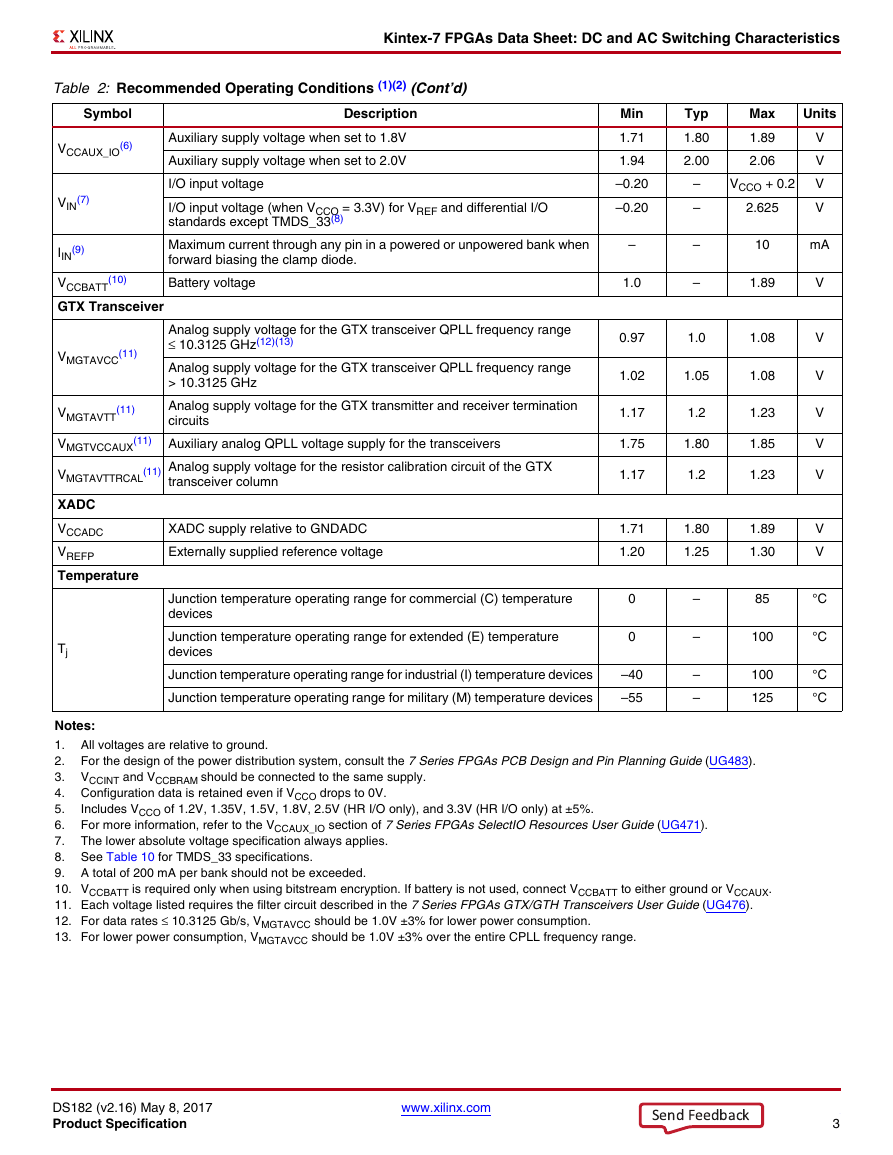
Table 2: Recommended Operating Conditions (1)(2) (Cont’d)
Symbol
VCCAUX_IO
(6)
Description
Auxiliary supply voltage when set to 1.8V
Auxiliary supply voltage when set to 2.0V
(7)
VIN
(9)
IIN
I/O input voltage
I/O input voltage (when VCCO = 3.3V) for VREF and differential I/O
standards except TMDS_33(8)
Maximum current through any pin in a powered or unpowered bank when
forward biasing the clamp diode.
(10)
VCCBATT
GTX Transceiver
Battery voltage
VMGTAVCC
(11)
Analog supply voltage for the GTX transceiver QPLL frequency range
≤ 10.3125 GHz(12)(13)
Analog supply voltage for the GTX transceiver QPLL frequency range
> 10.3125 GHz
VMGTAVTT
(11)
Analog supply voltage for the GTX transmitter and receiver termination
circuits
VMGTVCCAUX
(11) Auxiliary analog QPLL voltage supply for the transceivers
VMGTAVTTRCAL
transceiver column
(11) Analog supply voltage for the resistor calibration circuit of the GTX
XADC
VCCADC
VREFP
Temperature
XADC supply relative to GNDADC
Externally supplied reference voltage
Junction temperature operating range for commercial (C) temperature
devices
Tj
Junction temperature operating range for extended (E) temperature
devices
Junction temperature operating range for industrial (I) temperature devices
Junction temperature operating range for military (M) temperature devices
Min
1.71
1.94
–0.20
–0.20
–
1.0
0.97
1.02
1.17
1.75
1.17
1.71
1.20
0
0
–40
–55
Typ
1.80
2.00
–
–
–
–
1.0
1.05
1.2
1.80
1.2
1.80
1.25
–
–
–
–
Max
1.89
2.06
VCCO + 0.2
2.625
Units
V
V
V
V
10
mA
1.89
1.08
1.08
1.23
1.85
1.23
1.89
1.30
85
100
100
125
V
V
V
V
V
V
V
V
°C
°C
°C
°C
For the design of the power distribution system, consult the 7 Series FPGAs PCB Design and Pin Planning Guide (UG483).
Includes VCCO of 1.2V, 1.35V, 1.5V, 1.8V, 2.5V (HR I/O only), and 3.3V (HR I/O only) at ±5%.
For more information, refer to the VCCAUX_IO section of 7 Series FPGAs SelectIO Resources User Guide (UG471).
The lower absolute voltage specification always applies.
Notes:
1. All voltages are relative to ground.
2.
3. VCCINT and VCCBRAM should be connected to the same supply.
4. Configuration data is retained even if VCCO drops to 0V.
5.
6.
7.
8. See Table 10 for TMDS_33 specifications.
9. A total of 200 mA per bank should not be exceeded.
10. VCCBATT is required only when using bitstream encryption. If battery is not used, connect VCCBATT to either ground or VCCAUX.
11. Each voltage listed requires the filter circuit described in the 7 Series FPGAs GTX/GTH Transceivers User Guide (UG476).
12. For data rates ≤ 10.3125 Gb/s, VMGTAVCC should be 1.0V ±3% for lower power consumption.
13. For lower power consumption, VMGTAVCC should be 1.0V ±3% over the entire CPLL frequency range.
DS182 (v2.16) May 8, 2017
Product Specification
www.xilinx.com
3
Send Feedback�
Kintex-7 FPGAs Data Sheet: DC and AC Switching Characteristics
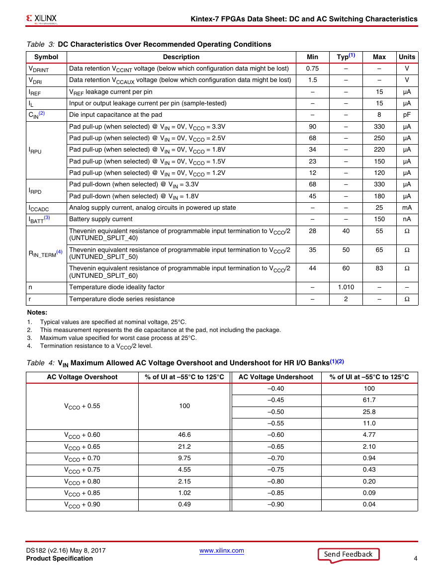
Table 3: DC Characteristics Over Recommended Operating Conditions
Symbol
Description
VDRINT
VDRI
IREF
IL
CIN
(2)
IRPU
IRPD
ICCADC
(3)
IBATT
RIN_TERM
(4)
Data retention VCCINT voltage (below which configuration data might be lost)
Data retention VCCAUX voltage (below which configuration data might be lost)
VREF leakage current per pin
Input or output leakage current per pin (sample-tested)
Die input capacitance at the pad
Pad pull-up (when selected) @ VIN = 0V, VCCO = 3.3V
Pad pull-up (when selected) @ VIN = 0V, VCCO = 2.5V
Pad pull-up (when selected) @ VIN = 0V, VCCO = 1.8V
Pad pull-up (when selected) @ VIN = 0V, VCCO = 1.5V
Pad pull-up (when selected) @ VIN = 0V, VCCO = 1.2V
Pad pull-down (when selected) @ VIN = 3.3V
Pad pull-down (when selected) @ VIN = 1.8V
Analog supply current, analog circuits in powered up state
Battery supply current
Thevenin equivalent resistance of programmable input termination to VCCO/2
(UNTUNED_SPLIT_40)
Thevenin equivalent resistance of programmable input termination to VCCO/2
(UNTUNED_SPLIT_50)
Thevenin equivalent resistance of programmable input termination to VCCO/2
(UNTUNED_SPLIT_60)
n
r
Temperature diode ideality factor
Temperature diode series resistance
Min
0.75
1.5
–
–
–
90
68
34
23
12
68
45
–
–
28
35
44
–
–
Typ(1)
Max
Units
–
–
–
–
–
–
–
–
–
–
–
–
–
–
40
50
60
1.010
2
–
–
15
15
8
330
250
220
150
120
330
180
25
150
55
65
83
–
–
V
V
µA
µA
pF
µA
µA
µA
µA
µA
µA
µA
mA
nA
Ω
Ω
Ω
–
Ω
Typical values are specified at nominal voltage, 25°C.
This measurement represents the die capacitance at the pad, not including the package.
Notes:
1.
2.
3. Maximum value specified for worst case process at 25°C.
4.
Termination resistance to a VCCO/2 level.
Table 4: VIN Maximum Allowed AC Voltage Overshoot and Undershoot for HR I/O Banks(1)(2)
AC Voltage Overshoot
% of UI at –55°C to 125°C
AC Voltage Undershoot
% of UI at –55°C to 125°C
VCCO + 0.55
VCCO + 0.60
VCCO + 0.65
VCCO + 0.70
VCCO + 0.75
VCCO + 0.80
VCCO + 0.85
VCCO + 0.90
100
46.6
21.2
9.75
4.55
2.15
1.02
0.49
–0.40
–0.45
–0.50
–0.55
–0.60
–0.65
–0.70
–0.75
–0.80
–0.85
–0.90
100
61.7
25.8
11.0
4.77
2.10
0.94
0.43
0.20
0.09
0.04
DS182 (v2.16) May 8, 2017
Product Specification
www.xilinx.com
4
Send Feedback�
Kintex-7 FPGAs Data Sheet: DC and AC Switching Characteristics
Table 4: VIN Maximum Allowed AC Voltage Overshoot and Undershoot for HR I/O Banks(1)(2) (Cont’d)
AC Voltage Overshoot
% of UI at –55°C to 125°C
AC Voltage Undershoot
% of UI at –55°C to 125°C
VCCO + 0.95
0.24
–0.95
0.02
Notes:
1. A total of 200 mA per bank should not be exceeded.
2.
The peak voltage of the overshoot or undershoot, and the duration above VCCO + 0.20V or below GND – 0.20V, must not exceed the values
in this table.
Table 5: VIN Maximum Allowed AC Voltage Overshoot and Undershoot for HP I/O Banks(1)(2)
AC Voltage Overshoot
% of UI at –55°C to 125°C
AC Voltage Undershoot
% of UI at –55°C to 125°C
VCCO + 0.55
VCCO + 0.60
VCCO + 0.65
VCCO + 0.70
VCCO + 0.75
VCCO + 0.80
VCCO + 0.85
VCCO + 0.90
VCCO + 0.95
100
50.0(3)
50.0(3)
47.0
21.2
9.71
4.51
2.12
1.01
–0.55
–0.60
–0.65
–0.70
–0.75
–0.80
–0.85
–0.90
–0.95
100
50.0(3)
50.0(3)
50.0(3)
50.0(3)
50.0(3)
28.4
12.7
5.79
Notes:
1. A total of 200 mA per bank should not be exceeded.
2.
The peak voltage of the overshoot or undershoot, and the duration above VCCO + 0.20V or below GND – 0.20V, must not exceed the values
in this table.
For UI lasting less than 20 µs.
3.
Table 6: Typical Quiescent Supply Current
Symbol
Description
Device
ICCINTQ
Quiescent VCCINT supply
current
XC7K70T
XC7K160T
XC7K325T
XC7K355T
XC7K410T
XC7K420T
XC7K480T
XQ7K325T
XQ7K410T
Speed Grade
-3
241
474
810
993
1080
1313
1313
N/A
N/A
-2/-2LE
241
474
810
993
1080
1313
1313
810
1080
1.0V
-1
241
474
810
993
1080
1313
1313
810
1080
-1LM
N/A
N/A
N/A
N/A
N/A
N/A
N/A
810
N/A
-1M
N/A
N/A
N/A
N/A
N/A
N/A
N/A
810
1080
0.95V
-2LI
0.9V
-2LE
Units
N/A
271
463
568
618
751
751
463
618
187
368
629
771
838
1019
1019
629
838
mA
mA
mA
mA
mA
mA
mA
mA
mA
DS182 (v2.16) May 8, 2017
Product Specification
www.xilinx.com
5
Send Feedback�
Kintex-7 FPGAs Data Sheet: DC and AC Switching Characteristics
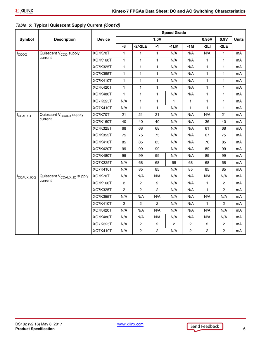
Table 6: Typical Quiescent Supply Current (Cont’d)
Symbol
Description
Device
Speed Grade
1.0V
-1
-1LM
-3
-2/-2LE
ICCOQ
Quiescent VCCO supply
current
ICCAUXQ
Quiescent VCCAUX supply
current
ICCAUX_IOQ Quiescent VCCAUX_IO supply
current
XC7K70T
XC7K160T
XC7K325T
XC7K355T
XC7K410T
XC7K420T
XC7K480T
XQ7K325T
XQ7K410T
XC7K70T
XC7K160T
XC7K325T
XC7K355T
XC7K410T
XC7K420T
XC7K480T
XQ7K325T
XQ7K410T
XC7K70T
XC7K160T
XC7K325T
XC7K355T
XC7K410T
XC7K420T
XC7K480T
XQ7K325T
XQ7K410T
1
1
1
1
1
1
1
N/A
N/A
21
40
68
75
85
99
99
N/A
N/A
N/A
2
2
N/A
2
N/A
N/A
N/A
N/A
1
1
1
1
1
1
1
1
1
21
40
68
75
85
99
99
68
85
1
1
1
1
1
1
1
1
1
21
40
68
75
85
99
99
68
85
N/A
N/A
2
2
N/A
2
N/A
N/A
2
2
2
2
N/A
2
N/A
N/A
2
2
N/A
N/A
N/A
N/A
N/A
N/A
N/A
1
N/A
N/A
N/A
N/A
N/A
N/A
N/A
N/A
68
N/A
N/A
N/A
N/A
N/A
N/A
N/A
N/A
2
N/A
-1M
N/A
N/A
N/A
N/A
N/A
N/A
N/A
1
1
N/A
N/A
N/A
N/A
N/A
N/A
N/A
68
85
N/A
N/A
N/A
N/A
N/A
N/A
N/A
2
2
0.95V
-2LI
N/A
1
1
1
1
1
1
1
1
N/A
36
61
67
76
89
89
68
85
1
1
1
1
1
1
1
1
1
21
40
68
75
85
99
99
68
85
N/A
N/A
1
1
N/A
1
N/A
N/A
2
2
2
2
N/A
2
N/A
N/A
2
2
Units
0.9V
-2LE
mA
mA
mA
mA
mA
mA
mA
mA
mA
mA
mA
mA
mA
mA
mA
mA
mA
mA
mA
mA
mA
mA
mA
mA
mA
mA
mA
DS182 (v2.16) May 8, 2017
Product Specification
www.xilinx.com
6
Send Feedback�
Kintex-7 FPGAs Data Sheet: DC and AC Switching Characteristics
Table 6: Typical Quiescent Supply Current (Cont’d)
Symbol
Description
Device
ICCBRAMQ
Quiescent VCCBRAM supply
current
XC7K70T
XC7K160T
XC7K325T
XC7K355T
XC7K410T
XC7K420T
XC7K480T
XQ7K325T
XQ7K410T
-3
6
14
19
31
34
41
41
N/A
N/A
Speed Grade
1.0V
-1
-1LM
-2/-2LE
6
14
19
31
34
41
41
19
34
6
14
19
31
34
41
41
19
34
N/A
N/A
N/A
N/A
N/A
N/A
N/A
19
N/A
0.95V
-2LI
N/A
8
10
17
19
23
23
19
34
Units
0.9V
-2LE
6
14
19
31
34
41
41
19
34
mA
mA
mA
mA
mA
mA
mA
mA
mA
-1M
N/A
N/A
N/A
N/A
N/A
N/A
N/A
19
34
Notes:
1.
2.
Typical values are specified at nominal voltage, 85°C junction temperatures (Tj) with single-ended SelectIO resources.
Typical values are for blank configured devices with no output current loads, no active input pull-up resistors, all I/O pins are 3-state and
floating.
3. Use the Xilinx Power Estimator (XPE) spreadsheet tool (download at www.xilinx.com/power) to estimate static power consumption for
conditions other than those specified.
Power-On/Off Power Supply Sequencing
The recommended power-on sequence is VCCINT, VCCBRAM, VCCAUX, VCCAUX_IO, and VCCO to achieve minimum current draw
and ensure that the I/Os are 3-stated at power-on. The recommended power-off sequence is the reverse of the power-on
sequence. If VCCINT and VCCBRAM have the same recommended voltage levels then both can be powered by the same supply
and ramped simultaneously. If VCCAUX, VCCAUX_IO, and VCCO have the same recommended voltage levels then they can be
powered by the same supply and ramped simultaneously.
For VCCO voltages of 3.3V in HR I/O banks and configuration bank 0:
•
The voltage difference between VCCO and VCCAUX must not exceed 2.625V for longer than TVCCO2VCCAUX for each
power-on/off cycle to maintain device reliability levels.
The TVCCO2VCCAUX time can be allocated in any percentage between the power-on and power-off ramps.
•
The recommended power-on sequence to achieve minimum current draw for the GTX transceivers is VCCINT, VMGTAVCC,
VMGTAVTT OR VMGTAVCC, VCCINT, VMGTAVTT. There is no recommended sequencing for VMGTVCCAUX. Both VMGTAVCC and VCCINT
can be ramped simultaneously. The recommended power-off sequence is the reverse of the power-on sequence to achieve
minimum current draw.
If these recommended sequences are not met, current drawn from VMGTAVTT can be higher than specifications during power-
up and power-down.
• When VMGTAVTT is powered before VMGTAVCC and VMGTAVTT – VMGTAVCC > 150 mV and VMGTAVCC < 0.7V, the VMGTAVTT
current draw can increase by 460 mA per transceiver during VMGTAVCC ramp up. The duration of the current draw can be
up to 0.3 x TMGTAVCC (ramp time from GND to 90% of VMGTAVCC). The reverse is true for power-down.
• When VMGTAVTT is powered before VCCINT and VMGTAVTT – VCCINT > 150 mV and VCCINT < 0.7V, the VMGTAVTT current
draw can increase by 50 mA per transceiver during VCCINT ramp up. The duration of the current draw can be up to
0.3 x TVCCINT (ramp time from GND to 90% of VCCINT). The reverse is true for power-down.
There is no recommended sequence for supplies not shown.
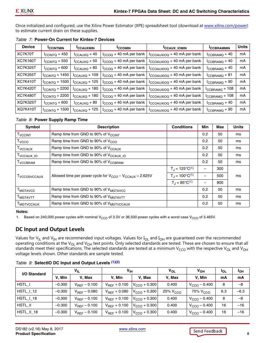
Table 7 shows the minimum current, in addition to ICCQ, that are required by Kintex-7 devices for proper power-on and
configuration. If the current minimums shown in Table 6 and Table 7 are met, the device powers on after all five supplies
have passed through their power-on reset threshold voltages. The FPGA must not be configured until after VCCINT is applied.
DS182 (v2.16) May 8, 2017
Product Specification
www.xilinx.com
7
Send Feedback�
Kintex-7 FPGAs Data Sheet: DC and AC Switching Characteristics
Once initialized and configured, use the Xilinx Power Estimator (XPE) spreadsheet tool (download at www.xilinx.com/power)
to estimate current drain on these supplies.
Table 7: Power-On Current for Kintex-7 Devices
Device
XC7K70T
XC7K160T
XC7K325T
XC7K355T
XC7K410T
XC7K420T
XC7K480T
XQ7K325T
XQ7K410T
ICCINTMIN
ICCAUXMIN
ICCAUXQ + 40
ICCINTQ + 450
ICCAUXQ + 50
ICCINTQ + 550
ICCAUXQ + 80
ICCINTQ + 600
ICCINTQ + 1450 ICCAUXQ + 109
ICCINTQ + 1500 ICCAUXQ + 125
ICCINTQ + 2200 ICCAUXQ + 180
ICCINTQ + 2200 ICCAUXQ + 180
ICCINTQ + 600
ICCAUXQ + 80
ICCINTQ + 1500 ICCAUXQ + 125
ICCOMIN
ICCAUX_IOMIN
ICCOQ + 40 mA per bank
ICCOQ + 40 mA per bank
ICCOQ + 40 mA per bank
ICCOQ + 40 mA per bank
ICCOQ + 40 mA per bank
ICCOQ + 40 mA per bank
ICCOQ + 40 mA per bank
ICCOQ + 40 mA per bank
ICCOQ + 40 mA per bank
ICCOAUXIOQ + 40 mA per bank
ICCOAUXIOQ + 40 mA per bank
ICCOAUXIOQ + 40 mA per bank
ICCOAUXIOQ + 40 mA per bank
ICCOAUXIOQ + 40 mA per bank
ICCOAUXIOQ + 40 mA per bank
ICCOAUXIOQ + 40 mA per bank
ICCOAUXIOQ + 40 mA per bank
ICCOAUXIOQ + 40 mA per bank
Units
mA
mA
ICCBRAMMIN
ICCBRAMQ + 40
ICCBRAMQ + 40
ICCBRAMQ + 40
ICCBRAMQ + 81
ICCBRAMQ + 90
mA
ICCBRAMQ + 108 mA
ICCBRAMQ + 108 mA
ICCBRAMQ + 40
mA
ICCBRAMQ + 90
mA
mA
mA
Table 8: Power Supply Ramp Time
Symbol
TVCCINT
TVCCO
TVCCAUX
TVCCAUX_IO
TVCCBRAM
Description
Ramp time from GND to 90% of VCCINT
Ramp time from GND to 90% of VCCO
Ramp time from GND to 90% of VCCAUX
Ramp time from GND to 90% of VCCAUX_IO
Ramp time from GND to 90% of VCCBRAM
TVCCO2VCCAUX
Allowed time per power cycle for VCCO – VCCAUX > 2.625V
TMGTAVCC
TMGTAVTT
TMGTVCCAUX
Ramp time from GND to 90% of VMGTAVCC
Ramp time from GND to 90% of VMGTAVTT
Ramp time from GND to 90% of VMGTVCCAUX
Conditions
Min
Max
Units
0.2
0.2
0.2
0.2
0.2
–
–
–
0.2
0.2
0.2
50
50
50
50
50
300
500
800
50
50
50
ms
ms
ms
ms
ms
ms
ms
ms
ms
TJ = 125°C(1)
TJ = 100°C(1)
TJ = 85°C(1)
Notes:
1. Based on 240,000 power cycles with nominal VCCO of 3.3V or 36,500 power cycles with a worst case VCCO of 3.465V.
DC Input and Output Levels
Values for VIL and VIH are recommended input voltages. Values for IOL and IOH are guaranteed over the recommended
operating conditions at the VOL and VOH test points. Only selected standards are tested. These are chosen to ensure that all
standards meet their specifications. The selected standards are tested at a minimum VCCO with the respective VOL and VOH
voltage levels shown. Other standards are sample tested.
Table 9: SelectIO DC Input and Output Levels (1)(2)
I/O Standard
HSTL_I
HSTL_I_12
HSTL_I_18
HSTL_II
HSTL_II_18
V, Min
–0.300
–0.300
–0.300
–0.300
–0.300
VIL
VIH
V, Max
V, Min
V, Max
VREF – 0.100
VREF – 0.080
VREF – 0.100
VREF – 0.100
VREF – 0.100
VREF + 0.100 VCCO + 0.300
VREF + 0.080 VCCO + 0.300
VREF + 0.100 VCCO + 0.300
VREF + 0.100 VCCO + 0.300
VREF + 0.100 VCCO + 0.300
VOL
V, Max
0.400
25% VCCO
0.400
0.400
0.400
VOH
V, Min
VCCO – 0.400
75% VCCO
VCCO – 0.400
VCCO – 0.400
VCCO – 0.400
IOL
mA
8
6.3
8
16
16
DS182 (v2.16) May 8, 2017
Product Specification
www.xilinx.com
IOH
mA
–8
–6.3
–8
–16
–16
8
Send Feedback�





 2023年江西萍乡中考道德与法治真题及答案.doc
 2012年重庆南川中考生物真题及答案.doc
 2013年江西师范大学地理学综合及文艺理论基础考研真题.doc
 2020年四川甘孜小升初语文真题及答案I卷.doc
 2020年注册岩土工程师专业基础考试真题及答案.doc
 2023-2024学年福建省厦门市九年级上学期数学月考试题及答案.doc
 2021-2022学年辽宁省沈阳市大东区九年级上学期语文期末试题及答案.doc
 2022-2023学年北京东城区初三第一学期物理期末试卷及答案.doc
 2018上半年江西教师资格初中地理学科知识与教学能力真题及答案.doc
 2012年河北国家公务员申论考试真题及答案-省级.doc
 2020-2021学年江苏省扬州市江都区邵樊片九年级上学期数学第一次质量检测试题及答案.doc
 2022下半年黑龙江教师资格证中学综合素质真题及答案.doc