NMOS and PMOS Linear Voltage Regulators
Course Objective:
To be able to explain the differences between NMOS and PMOS Linear Voltage Regulators; their basic operation, advantages and limitations, as
well as identifing applications where one, or the other, would be appropriate choice.
Course Map/Table of Contents
1. Course Navigation
1.
1.1 Course Navigation
2. Linear Voltage Regulator Basics
1.
2.
3.
4.
5.
6.
7.
8.
9.
10.
2.1 Introduction
2.2 The Linear Voltage Regulator
2.3 Simple Model
2.4 Simple Model, with variables
2.5 Simple Model, with values
2.6 Simple Model, with a change of Load Current
2.7 Simple Model, with a change in Input Voltage
2.8 The Control Loop
2.9 Simple Model, with Control Loop blocks
2.10 The Basic Real-World Model
3. So what's the difference?
1.
2.
3.
4.
3.1 The Bipolar model
3.2 The Bipolar model
3.3 The CMOS model
3.4 The CMOS model
4. Types of NMOS and PMOS Linear Voltage Regulators
1.
2.
3.
4.
4.1 Two Types
4.2 Standard Regulator
4.3 LDO Regulators
4.4 The Differences to consider
5. Standard NMOS Voltage Regulators
1.
2.
3.
4.
5.
6.
7.
8.
5.1 Introduction to the standard NMOS
5.2 Losses in the standard NMOS
5.3 Simple Model of losses in the standard NMOS
5.4 Driving the standard NMOS Pass Element
5.5 NMOS Gate Drive vs Low Load Current
5.6 NMOS Gate Drive vs High Load Current
5.7 Standard NMOS Output Capacitor Requirements
5.8 Standard NMOS Summary
6. NMOS "Dual-Rail" Voltage regulators
1.
2.
3.
4.
5.
6.
7.
8.
6.1 Introduction to NMOS "Dual-Rail" Voltage Regulator
6.2 Losses in the NMOS "Dual-Rail"
6.3 Simple Model of Losses in the NMOS "Dual-Rail" LDO
6.4 Driving the NMOS "Dual-Rail" Pass Element
6.5 Gate Drive vs Low Load Current
6.6 Gate Drive vs High Load Current
6.7 NMOS 'Dual-Rail' Output Capacitor Requirements
6.8 Summary
7. PMOS LDO Voltage Regulators
1.
2.
3.
4.
5.
6.
7.
7.1 Introduction to PMOS LDO Voltage Regulators
7.2 Losses in the PMOS LDO drive circuitry
7.3 Simple Model of Losses in the PMOS LDO Regulator
7.4 Driving the PMOS LDO Pass Element
7.5 Gate Drive vs Low Load Current
7.6 Gate Drive vs High Load Current
7.7 PMOS LDO Output Capacitor Requirements
NMOS and PMOS Linear Voltage Regulators Copyright © 2010 by National Semiconductor Corporation All rights reserved
�
8.
7.8 Summary
8. Package Thermals
1.
2.
3.
4.
5.
6.
8.1 Package Limitations
8.2 Power Dissipation Variables
8.3 Power Dissipation Calculation
8.4 Junction Temperature Rise
8.5 Maximum Ambient Temperature
8.6 The Operating Junction Temperature
9. Summary
1.
2.
9.1 Summary
9.2 Selecting the Best Regulator For Your Application
1. Course Navigation
1.1 Course Navigation
1.1 Course Navigation
This course is organized like a book with multiple chapters. Each chapter may have one or more pages.
The previous and next arrows move you forward and back through the course page by page.
The left navigation bar takes you to any chapter. It also contains the bookmarking buttons, 'save' and 'go to.' To save your place
in a course, press the 'save' button. The next time you open the course, clicking on 'go to' will take you to the page you saved or
bookmarked.
The top services bar contains additional information such as glossary of terms, who to go to for help with this subject and an
FAQ. Clicking home on this bar will take you back to the course beginning.
Don't miss the hints, references, exercises and quizzes which appear at the bottom of some pages.
2. Linear Voltage Regulator Basics
This chapter will discuss how a linear voltage regulator works
2.1 Introduction
2.2 The Linear Voltage Regulator
2.3 Simple Model
2.4 Simple Model, with variables
2.5 Simple Model, with values
2.6 Simple Model, with a change of Load Current
2.7 Simple Model, with a change in Input Voltage
2.8 The Control Loop
2.9 Simple Model, with Control Loop blocks
2.10 The Basic Real-World Model
2.1 Introduction
What is a voltage regulator?
�
Every electronic circuit is designed to operate off of some supply voltage, which is usually assumed to be constant.
A Linear Voltage Regulator provides this constant DC output voltage and contains circuitry that continuously holds the output voltage at
the design value regardless of changes in load current or input voltage.
This assumes that the load current and input voltage are within the specified operating range for the device.
The linear regulator is the basic building block of nearly every power supply used in electronics.
The IC linear regulator is so easy to use that it is virtually foolproof, and so inexpensive that it is usually one of the cheapest
components in an electronic assembly.
Linear Voltage Regulators are 'step-down' devices, that is the output voltage is always lower than the input voltage.
2.2 The Linear Voltage Regulator
What is a Linear Voltage Regulator?
A linear regulator operates by using a voltage-controlled current source to force a fixed voltage to appear at the regulator output
terminal.
The control circuitry continuosly monitors (senses) the output voltage, and adjusts the current source (as required by the load) to hold
the output voltage at the desired value.
The design limit of the current source defines the maximum load current the regulator can source and still maintain regulation.
The output voltage is controlled using a feedback loop, which requires some type of compensation to assure loop stability.
Most linear regulators have built-in compensation, and are completely stable without external components.
Some regulators (like Low-Dropout types), do require some external capacitance connected from the output lead to ground to assure
regulator stability.
2.3 Simple Model
A basic (first order) linear voltage regulator can be modeled with two resistors and a power supply for VIN .
Knowing the required output voltage (VOUT ), the load current (ILOAD ), along with the input voltage (VIN ), is essential to creating the
model.
2.4 Simple Model, with variables
�
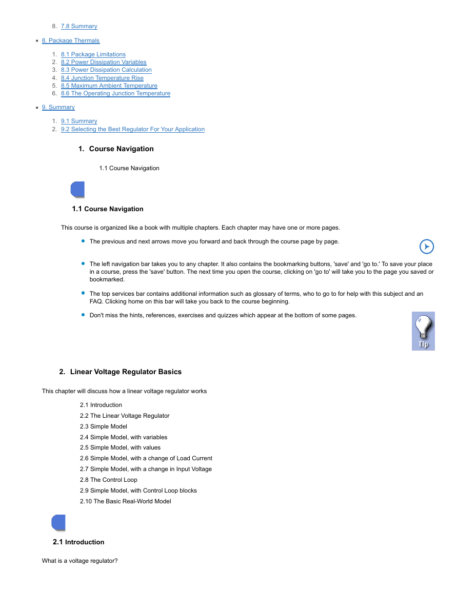
In reality, the only constant is the output voltage, VOUT.
Everything else can, and will, be constantly changing.
The input voltage may have changes due to outside influences, the load current may change due to a dynamic change in the behaviour of the
load.
Changes in these variables can all happen simultaneously, and the value needed for RPASS to hold VOUT at a constant value will need to change
as well.
2.5 Simple Model, with values
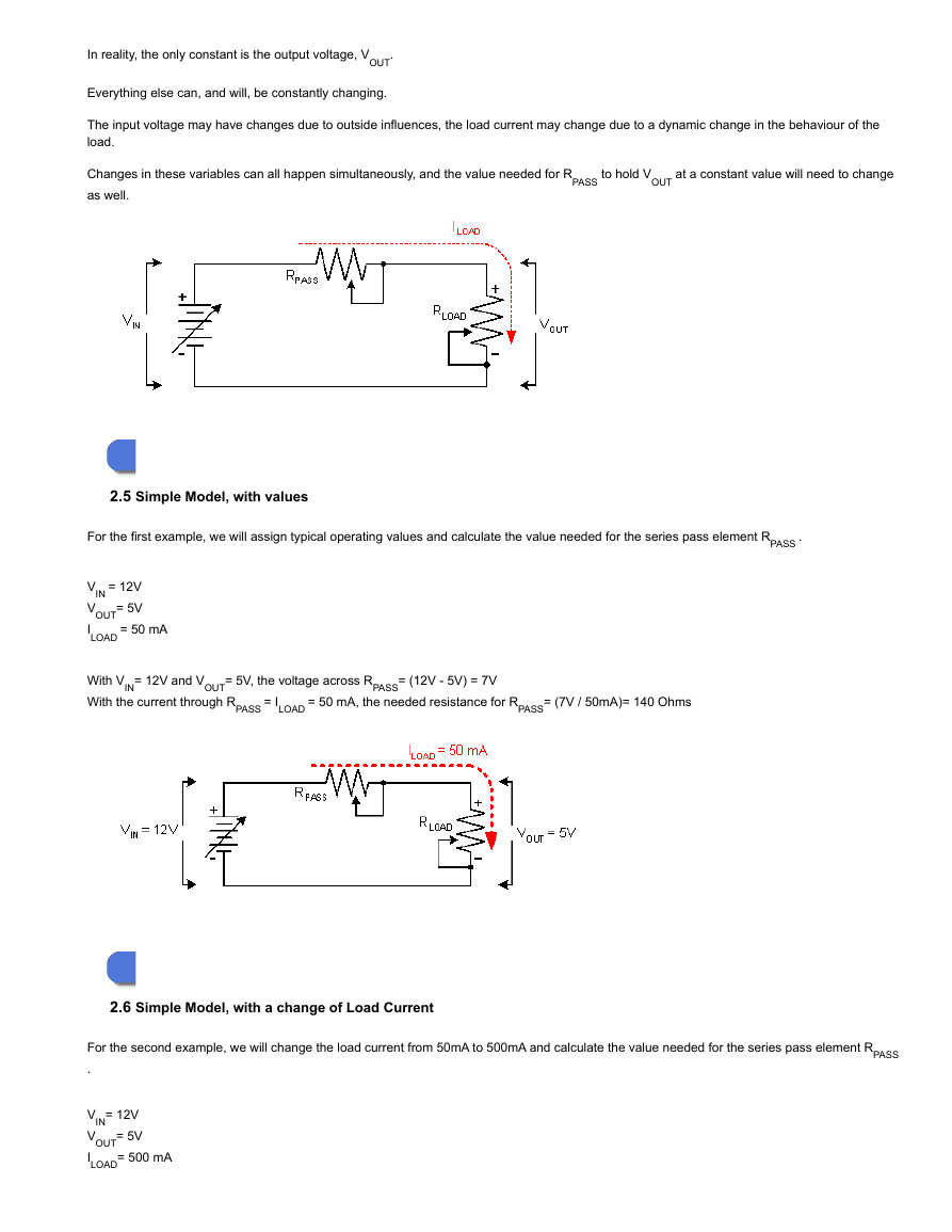
For the first example, we will assign typical operating values and calculate the value needed for the series pass element RPASS .
VIN = 12V
VOUT= 5V
ILOAD = 50 mA
With VIN= 12V and VOUT= 5V, the voltage across RPASS= (12V - 5V) = 7V
With the current through RPASS = ILOAD = 50 mA, the needed resistance for RPASS= (7V / 50mA)= 140 Ohms
2.6 Simple Model, with a change of Load Current
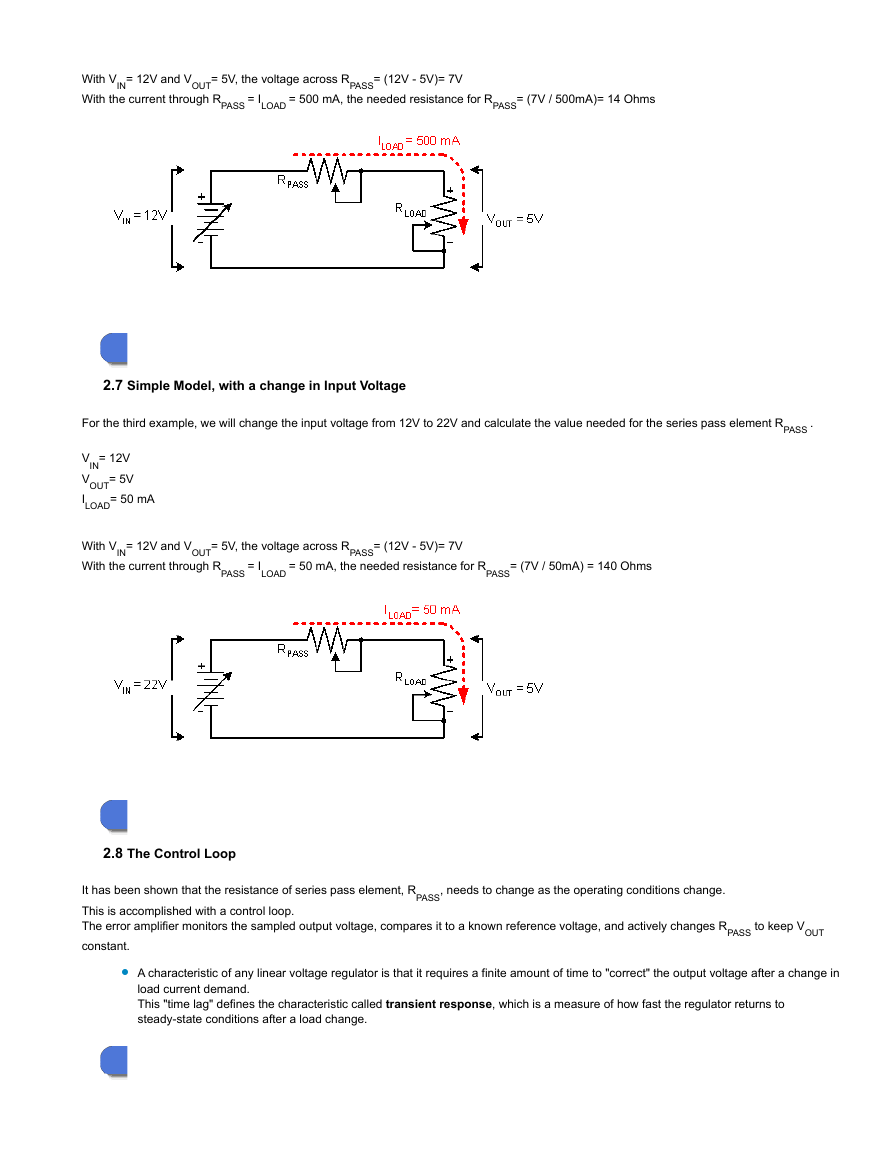
For the second example, we will change the load current from 50mA to 500mA and calculate the value needed for the series pass element RPASS
.
VIN= 12V
VOUT= 5V
ILOAD= 500 mA
�
With VIN= 12V and VOUT= 5V, the voltage across RPASS= (12V - 5V)= 7V
With the current through RPASS = ILOAD = 500 mA, the needed resistance for RPASS= (7V / 500mA)= 14 Ohms
2.7 Simple Model, with a change in Input Voltage
For the third example, we will change the input voltage from 12V to 22V and calculate the value needed for the series pass element RPASS .
VIN= 12V
VOUT= 5V
ILOAD= 50 mA
With VIN= 12V and VOUT= 5V, the voltage across RPASS= (12V - 5V)= 7V
With the current through RPASS = ILOAD = 50 mA, the needed resistance for RPASS= (7V / 50mA) = 140 Ohms
2.8 The Control Loop
It has been shown that the resistance of series pass element, RPASS, needs to change as the operating conditions change.
This is accomplished with a control loop.
The error amplifier monitors the sampled output voltage, compares it to a known reference voltage, and actively changes RPASS to keep VOUT
constant.
A characteristic of any linear voltage regulator is that it requires a finite amount of time to "correct" the output voltage after a change in
load current demand.
This "time lag" defines the characteristic called transient response, which is a measure of how fast the regulator returns to
steady-state conditions after a load change.
�
2.9 Simple Model, with Control Loop blocks
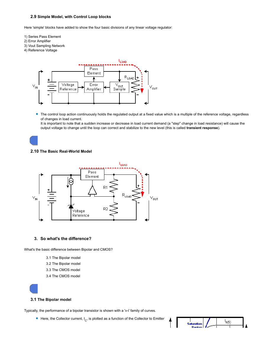
Here 'simple' blocks have added to show the four basic divisions of any linear voltage regulator:
1) Series Pass Element
2) Error Amplifier
3) Vout Sampling Network
4) Reference Voltage
The control loop action continuously holds the regulated output at a fixed value which is a multiple of the reference voltage, regardless
of changes in load current.
It is important to note that a sudden increase or decrease in load current demand (a "step" change in load resistance) will cause the
output voltage to change until the loop can correct and stabilize to the new level (this is called transient response).
2.10 The Basic Real-World Model
3. So what's the difference?
What's the basic difference between Bipolar and CMOS?
3.1 The Bipolar model
3.2 The Bipolar model
3.3 The CMOS model
3.4 The CMOS model
3.1 The Bipolar model
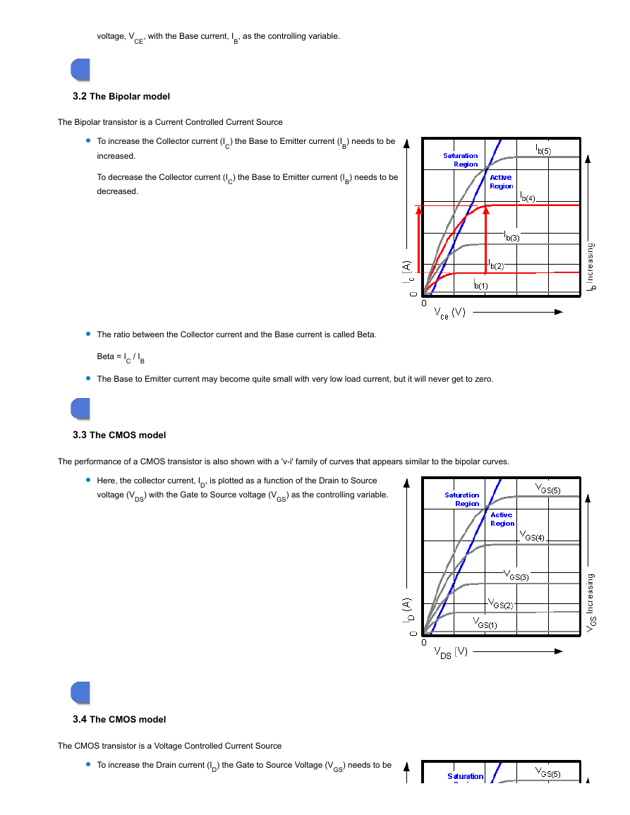
Typically, the performance of a bipolar transistor is shown with a 'v-i' family of curves.
Here, the Collector current, IC, is plotted as a function of the Collector to Emitter
�
voltage, VCE, with the Base current, IB, as the controlling variable.
3.2 The Bipolar model
The Bipolar transistor is a Current Controlled Current Source
To increase the Collector current (IC) the Base to Emitter current (IB) needs to be
increased.
To decrease the Collector current (IC) the Base to Emitter current (IB) needs to be
decreased.
The ratio between the Collector current and the Base current is called Beta.
Beta = IC / IB
The Base to Emitter current may become quite small with very low load current, but it will never get to zero.
3.3 The CMOS model
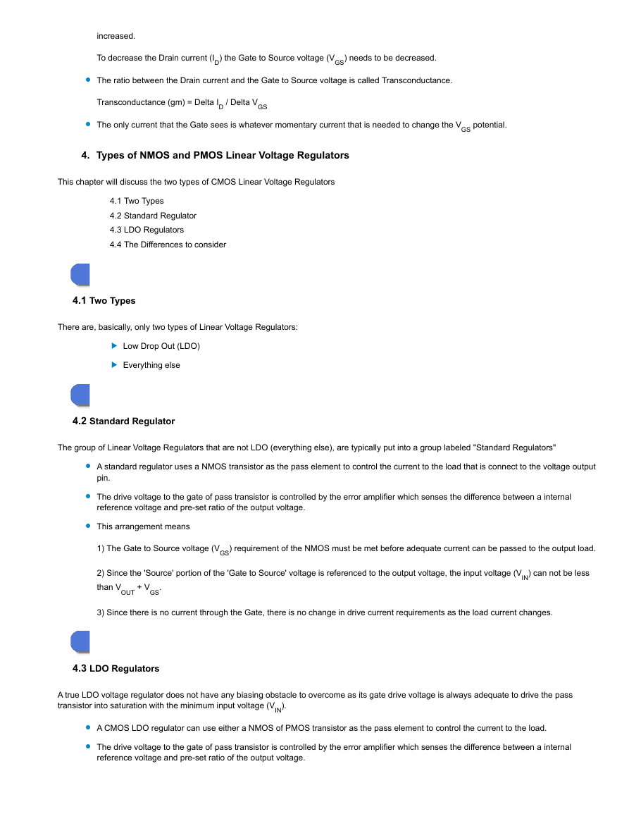
The performance of a CMOS transistor is also shown with a 'v-i' family of curves that appears similar to the bipolar curves.
Here, the collector current, ID, is plotted as a function of the Drain to Source
voltage (VDS) with the Gate to Source voltage (VGS) as the controlling variable.
3.4 The CMOS model
The CMOS transistor is a Voltage Controlled Current Source
To increase the Drain current (ID) the Gate to Source Voltage (VGS) needs to be
�
increased.
To decrease the Drain current (ID) the Gate to Source voltage (VGS) needs to be decreased.
The ratio between the Drain current and the Gate to Source voltage is called Transconductance.
Transconductance (gm) = Delta ID / Delta VGS
The only current that the Gate sees is whatever momentary current that is needed to change the VGS potential.
4. Types of NMOS and PMOS Linear Voltage Regulators
This chapter will discuss the two types of CMOS Linear Voltage Regulators
4.1 Two Types
4.2 Standard Regulator
4.3 LDO Regulators
4.4 The Differences to consider
4.1 Two Types
There are, basically, only two types of Linear Voltage Regulators:
Low Drop Out (LDO)
Everything else
4.2 Standard Regulator
The group of Linear Voltage Regulators that are not LDO (everything else), are typically put into a group labeled "Standard Regulators"
A standard regulator uses a NMOS transistor as the pass element to control the current to the load that is connect to the voltage output
pin.
The drive voltage to the gate of pass transistor is controlled by the error amplifier which senses the difference between a internal
reference voltage and pre-set ratio of the output voltage.
This arrangement means
1) The Gate to Source voltage (VGS) requirement of the NMOS must be met before adequate current can be passed to the output load.
2) Since the 'Source' portion of the 'Gate to Source' voltage is referenced to the output voltage, the input voltage (VIN) can not be less
than VOUT + VGS.
3) Since there is no current through the Gate, there is no change in drive current requirements as the load current changes.
4.3 LDO Regulators
A true LDO voltage regulator does not have any biasing obstacle to overcome as its gate drive voltage is always adequate to drive the pass
transistor into saturation with the minimum input voltage (VIN).
A CMOS LDO regulator can use either a NMOS of PMOS transistor as the pass element to control the current to the load.
The drive voltage to the gate of pass transistor is controlled by the error amplifier which senses the difference between a internal
reference voltage and pre-set ratio of the output voltage.
�



 2023年江西萍乡中考道德与法治真题及答案.doc
 2012年重庆南川中考生物真题及答案.doc
 2013年江西师范大学地理学综合及文艺理论基础考研真题.doc
 2020年四川甘孜小升初语文真题及答案I卷.doc
 2020年注册岩土工程师专业基础考试真题及答案.doc
 2023-2024学年福建省厦门市九年级上学期数学月考试题及答案.doc
 2021-2022学年辽宁省沈阳市大东区九年级上学期语文期末试题及答案.doc
 2022-2023学年北京东城区初三第一学期物理期末试卷及答案.doc
 2018上半年江西教师资格初中地理学科知识与教学能力真题及答案.doc
 2012年河北国家公务员申论考试真题及答案-省级.doc
 2020-2021学年江苏省扬州市江都区邵樊片九年级上学期数学第一次质量检测试题及答案.doc
 2022下半年黑龙江教师资格证中学综合素质真题及答案.doc