logo资料库

OV2778-Preliminary-Specification-a-CSP_Version-1-02_WPI.pdf

第1页 / 共150页
第2页 / 共150页
第3页 / 共150页
第4页 / 共150页
第5页 / 共150页
第6页 / 共150页
第7页 / 共150页
第8页 / 共150页
资料共150页,剩余部分请下载后查看
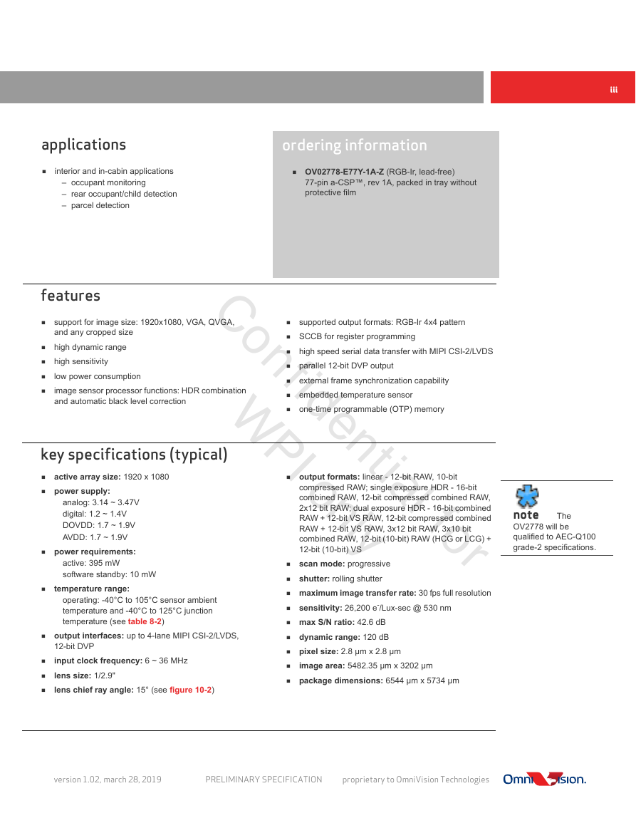
applications
features
key specifications (typical)
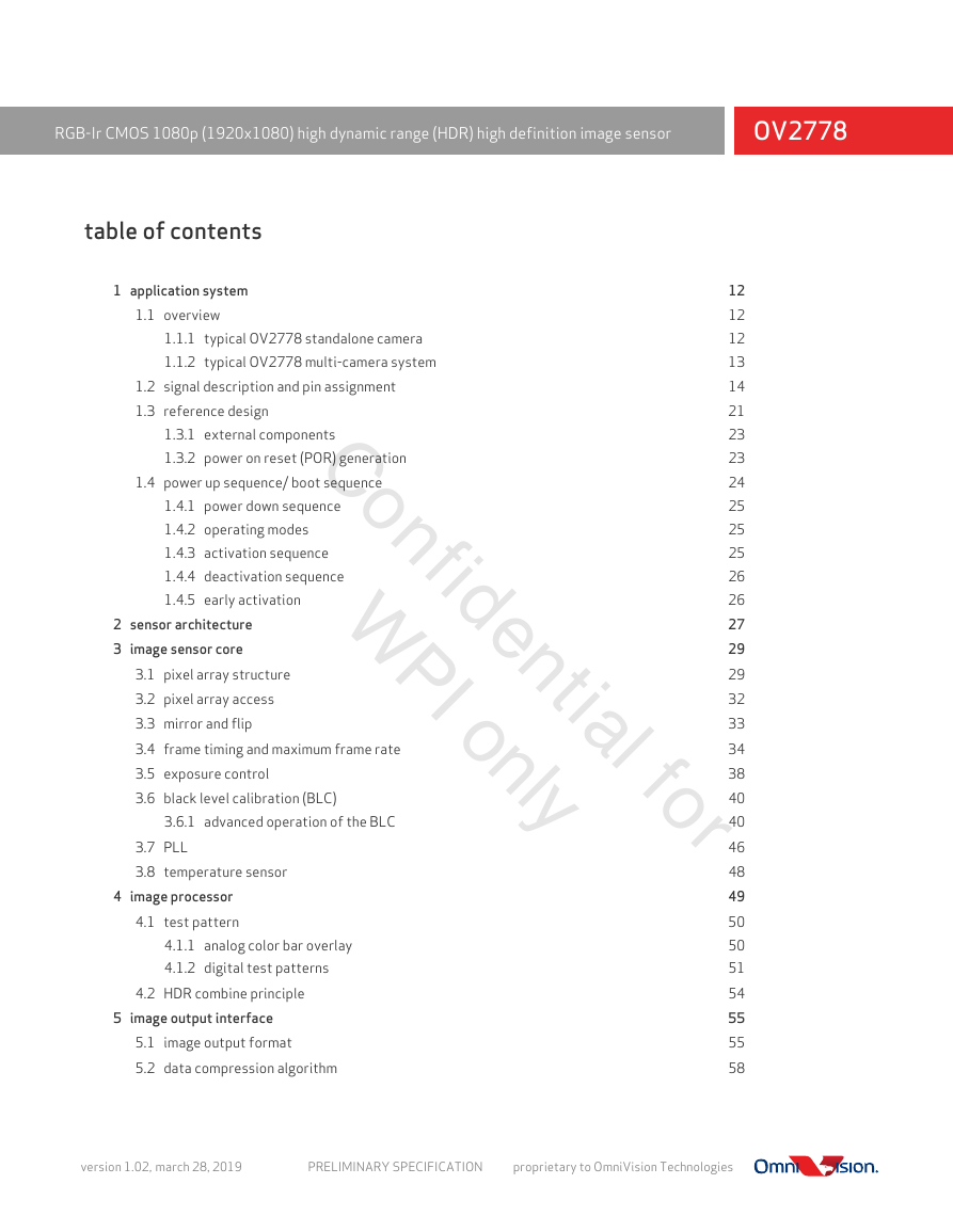
table of contents
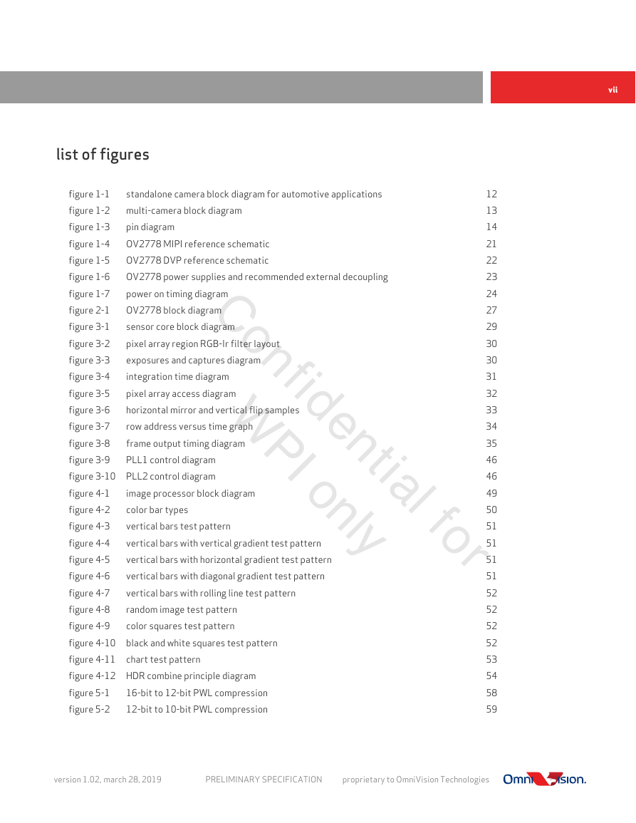
list of figures
list of tables
1 application system
1.1 overview
1.1.1 typical OV2778 standalone camera
figure 1-1 standalone camera block diagram for automotive applications
1.1.2 typical OV2778 multi-camera system
figure 1-2 multi-camera block diagram
1.2 signal description and pin assignment
figure 1-3 pin diagram
table 1-1 signal descriptions (sheet 1 of 3)
table 1-2 pin states under various conditions (sheet 1 of 2)
table 1-3 GPIO control registers (sheet 1 of 2)
table 1-4 pad equivalent circuit (sheet 1 of 2)
1.3 reference design
figure 1-4 OV2778 MIPI reference schematic
figure 1-5 OV2778 DVP reference schematic
1.3.1 external components
figure 1-6 OV2778 power supplies and recommended external decoupling
1.3.2 power on reset (POR) generation
1.4 power up sequence/ boot sequence
figure 1-7 power on timing diagram
table 1-5 power on timing
1.4.1 power down sequence
1.4.2 operating modes
1.4.3 activation sequence
1.4.4 deactivation sequence
1.4.5 early activation
2 sensor architecture
figure 2-1 OV2778 block diagram
3 image sensor core
figure 3-1 sensor core block diagram
3.1 pixel array structure
figure 3-2 pixel array region RGB-Ir filter layout
figure 3-3 exposures and captures diagram
figure 3-4 integration time diagram
3.2 pixel array access
figure 3-5 pixel array access diagram
3.3 mirror and flip
table 3-1 register setting for mirror
figure 3-6 horizontal mirror and vertical flip samples
3.4 frame timing and maximum frame rate
figure 3-7 row address versus time graph
figure 3-8 frame output timing diagram
table 3-2 supported output formats and frame rates for MIPI/LVDS
table 3-3 supported output formats and frame rates for DVP
table 3-4 timing control registers (sheet 1 of 2)
3.5 exposure control
table 3-5 exposure control registers
3.6 black level calibration (BLC)
3.6.1 advanced operation of the BLC
table 3-6 BLC control registers (sheet 1 of 5)
3.7 PLL
figure 3-9 PLL1 control diagram
figure 3-10 PLL2 control diagram
table 3-7 PLL control registers (sheet 1 of 2)
3.8 temperature sensor
table 3-8 temperature sensor registers
4 image processor
figure 4-1 image processor block diagram
4.1 test pattern
4.1.1 analog color bar overlay
figure 4-2 color bar types
4.1.2 digital test patterns
figure 4-3 vertical bars test pattern
figure 4-4 vertical bars with vertical gradient test pattern
figure 4-5 vertical bars with horizontal gradient test pattern
figure 4-6 vertical bars with diagonal gradient test pattern
figure 4-7 vertical bars with rolling line test pattern
figure 4-8 random image test pattern
figure 4-9 color squares test pattern
figure 4-10 black and white squares test pattern
figure 4-11 chart test pattern
table 4-1 test pattern control registers
4.2 HDR combine principle
figure 4-12 HDR combine principle diagram
table 4-2 combine control registers
5 image output interface
5.1 image output format
table 5-1 image output format summary
table 5-2 interface control register
table 5-3 register setting for different output formats
5.2 data compression algorithm
5.2.1 16b to 12b
figure 5-1 16-bit to 12-bit PWL compression
5.2.2 12b to 10b
figure 5-2 12-bit to 10-bit PWL compression
5.3 HDR output
5.3.1 MIPI
figure 5-3 non-staggered HDR with MIPI virtual channel diagram
figure 5-4 non-staggered HDR with MIPI virtual channel detail diagram
figure 5-5 staggered HDR with MIPI virtual channel diagram
figure 5-6 staggered HDR with MIPI virtual channel detail diagram
figure 5-7 non-staggered HDR without MIPI virtual channel overview diagram
figure 5-8 non-staggered HDR without MIPI virtual channel detail diagram
figure 5-9 staggered HDR without MIPI virtual channel overview diagram
figure 5-10 staggered HDR without MIPI virtual channel detail diagram
table 5-4 supported output formats and frame rates for MIPI
table 5-5 MIPI RAW image data types
figure 5-11 12b linear mode diagram
figure 5-12 10b linear mode diagram
figure 5-13 16b DCG + 12b dual HDR diagram
figure 5-14 12b compressed DCG + 12b dual HDR diagram
figure 5-15 3x12b (3x10b) DCG dual HDR diagram
figure 5-16 12b (10b) RAW DCG (HCG or LCG) + 12b (10b) VS dual HDR diagram
figure 5-17 16b DCG single HDR diagram
figure 5-18 12b compressed DCG single HDR diagram
figure 5-19 2x12b DCG single HDR diagram
table 5-6 MIPI control registers (sheet 1 of 10)
5.3.2 LVDS
figure 5-20 staggered HDR with LVDS dedicated lane (4-lane) diagram
figure 5-21 staggered HDR with LVDS dedicated lane (2-lane) diagram
table 5-7 supported output formats and frame rates for LVDS
figure 5-22 12 bits linear mode diagram
figure 5-23 10 bits linear mode diagram
figure 5-24 16b DCG + 12b dual HDR diagram
figure 5-25 12b compressed DCG + 12b dual HDR diagram
figure 5-26 3x12b (3x10b) DCG dual HDR diagram
figure 5-27 12b (10b) RAW DCG (HCG or LCG) + 12b (10b) VS dual HDR diagram
figure 5-28 16b DCG single HDR diagram
figure 5-29 12b compressed DCG single HDR diagram
figure 5-30 2x12b DCG single HDR diagram
table 5-8 LVDS control registers
5.3.3 DVP
figure 5-31 DVP diagram
figure 5-32 DVP setup/hold time diagram
table 5-9 DVP setup/hold time
figure 5-33 DVP timing diagram
figure 5-34 staggered HDR with DVP diagram
table 5-10 supported output formats and frame rates for DVP
figure 5-35 12 bits linear mode diagram
figure 5-36 10 bits linear mode diagram
figure 5-37 12b RAW DCG (HCG or LCG) + 12b VS diagram
figure 5-38 single exposure HDR diagram
figure 5-39 2x12b DCG single HDR diagram
table 5-11 DVP control registers (sheet 1 of 2)
5.4 instructions for backend control
5.4.1 VS data path delay
figure 5-40 sensor frame control signals diagram
table 5-12 VS data path delay register s
5.5 register writing
5.5.1 suggestion for writing register value just after VSYNC or FS
5.6 embedded data
5.6.1 embedded data format at output
figure 5-41 embedded data layout diagram
table 5-13 embedded data registers
5.7 group hold
table 5-14 group hold control registers (sheet 1 of 2)
5.8 cyclic redundancy check
5.8.1 embedded data
5.8.2 SCCB communication
table 5-15 SCCB CRC registers
6 SCCB interface
6.1 SCCB timing
figure 6-1 SCCB interface timing
table 6-1 SCCB interface timing specifications
6.2 direct access mode
6.2.1 message format
figure 6-2 message type
6.2.2 read / write operation
figure 6-3 SCCB single read from random location
figure 6-4 SCCB single read from current location
figure 6-5 SCCB sequential read from random location
figure 6-6 SCCB sequential read from current location
figure 6-7 SCCB single write to random location
figure 6-8 SCCB sequential write to random location
7 OTP memory
7.1 OTP memory map
table 7-1 OTP memory map overview
8 operating specifications
8.1 absolute maximum ratings
table 8-1 absolute maximum ratings
8.2 functional temperature
table 8-2 functional temperature
8.3 DC characteristics
table 8-3 DC characteristics (-40°C < TJ < 125°C)
8.4 AC characteristics
table 8-4 timing characteristics
9 mechanical specifications
9.1 physical specifications
figure 9-1 package specifications
table 9-1 package dimensions
9.2 IR reflow specifications
figure 9-2 IR reflow ramp rate requirements
table 9-2 reflow conditions
9.3 protective film specifications
figure 9-3 protective film specifications
10 optical specifications
10.1 sensor array center
figure 10-1 sensor array center
10.2 lens chief ray angle (CRA)
figure 10-2 chief ray angle (CRA)
table 10-1 CRA versus image height plot (sheet 1 of 2)
appendix A register table
A.1 module name and address range
A.2 device control registers
revision history
datasheet PRELIMINARY SPECIFICATION 1/2.9" RGB-Ir CMOS 1080p (1920 x 1080) high dynamic range (HDR) high definition (HD) image sensor 8 7 7 2 V O Confidential forWPI onlyPowered by TCPDF (www.tcpdf.org)
RGB-Ir CMOS 1080p (1920x1080) high dynamic range (HDR) high definition image sensor OV2778 00Copyright ©2019 OmniVision Technologies, Inc. All rights reserved. This document is provided “as is” with no warranties whatsoever, including any warranty of merchantability, non-infringement, fitness for any particular purpose, or any warranty otherwise arising out of any proposal, specification, or sample. OmniVision Technologies, Inc. and all its affiliates disclaim all liability, including liability for infringement of any proprietary rights, relating to the use of information in this document. No license, expressed or implied, by estoppel or otherwise, to any intellectual property rights is granted herein. The information contained in this document is considered proprietary to OmniVision Technologies, Inc. and all its affiliates. This information may be distributed to individuals or organizations authorized by OmniVision Technologies, Inc. to receive said information. Individuals and/or organizations are not allowed to re-distribute said information. Trademark Information OmniVision and the OmniVision logo are registered trademarks of OmniVision Technologies, Inc. OmniBSI-2 and a-CSP are trademarks of OmniVision Technologies, Inc. All other trademarks used herein are the property of their respective owners. RGB-Ir CMOS 1080p (1920x1080) high dynamic range (HDR) high definition image sensor datasheet (a-CSP) PRELIMINARY SPECIFICATION version 1.02 march 2019 To learn more about OmniVision Technologies, visit www.ovt.com. Confidential forWPI onlyPowered by TCPDF (www.tcpdf.org)
iii note The OV2778 will be qualified to AEC-Q100 grade-2 specifications. 00applications interior and in-cabin applications – occupant monitoring – rear occupant/child detection – parcel detection ordering information OV02778-E77Y-1A-Z (RGB-Ir, lead-free) 77-pin a-CSP™, rev 1A, packed in tray without protective film 00features support for image size: 1920x1080, VGA, QVGA, and any cropped size high dynamic range high sensitivity low power consumption image sensor processor functions: HDR combination and automatic black level correction supported output formats: RGB-Ir 4x4 pattern SCCB for register programming high speed serial data transfer with MIPI CSI-2/LVDS parallel 12-bit DVP output external frame synchronization capability embedded temperature sensor one-time programmable (OTP) memory 00key specifications (typical) active array size: 1920 x 1080 power supply: analog: 3.14 ~ 3.47V digital: 1.2 ~ 1.4V DOVDD: 1.7 ~ 1.9V AVDD: 1.7 ~ 1.9V power requirements: active: 395 mW software standby: 10 mW temperature range: operating: -40°C to 105°C sensor ambient temperature and -40°C to 125°C junction temperature (see table 8-2) output interfaces: up to 4-lane MIPI CSI-2/LVDS, 12-bit DVP input clock frequency: 6 ~ 36 MHz lens size: 1/2.9" lens chief ray angle: 15° (see figure 10-2) output formats: linear - 12-bit RAW, 10-bit compressed RAW; single exposure HDR - 16-bit combined RAW, 12-bit compressed combined RAW, 2x12 bit RAW; dual exposure HDR - 16-bit combined RAW + 12-bit VS RAW, 12-bit compressed combined RAW + 12-bit VS RAW, 3x12 bit RAW, 3x10 bit combined RAW, 12-bit (10-bit) RAW (HCG or LCG) + 12-bit (10-bit) VS scan mode: progressive shutter: rolling shutter maximum image transfer rate: 30 fps full resolution sensitivity: 26,200 e-/Lux-sec @ 530 nm max S/N ratio: 42.6 dB dynamic range: 120 dB pixel size: 2.8 µm x 2.8 µm image area: 5482.35 μm x 3202 μm package dimensions: 6544 μm x 5734 μm version 1.02, march 28, 2019 PRELIMINARY SPECIFICATION proprietary to OmniVision Technologies Confidential forWPI onlyPowered by TCPDF (www.tcpdf.org)
RGB-Ir CMOS 1080p (1920x1080) high dynamic range (HDR) high definition image sensor OV2778 00table of contents 1 application system 1.1 overview 1.1.1 typical OV2778 standalone camera 1.1.2 typical OV2778 multi-camera system 1.2 signal description and pin assignment 1.3 reference design 1.3.1 external components 1.3.2 power on reset (POR) generation 1.4 power up sequence/ boot sequence 1.4.1 power down sequence 1.4.2 operating modes 1.4.3 activation sequence 1.4.4 deactivation sequence 1.4.5 early activation 2 sensor architecture 3 image sensor core 3.1 pixel array structure 3.2 pixel array access 3.3 mirror and flip 3.4 frame timing and maximum frame rate 3.5 exposure control 3.6 black level calibration (BLC) 3.6.1 advanced operation of the BLC 3.7 PLL 3.8 temperature sensor 4 image processor 4.1 test pattern 4.1.1 analog color bar overlay 4.1.2 digital test patterns 4.2 HDR combine principle 5 image output interface 5.1 image output format 5.2 data compression algorithm 12 12 12 13 14 21 23 23 24 25 25 25 26 26 27 29 29 32 33 34 38 40 40 46 48 49 50 50 51 54 55 55 58 version 1.02, march 28, 2019 PRELIMINARY SPECIFICATION proprietary to OmniVision Technologies Confidential forWPI onlyPowered by TCPDF (www.tcpdf.org)
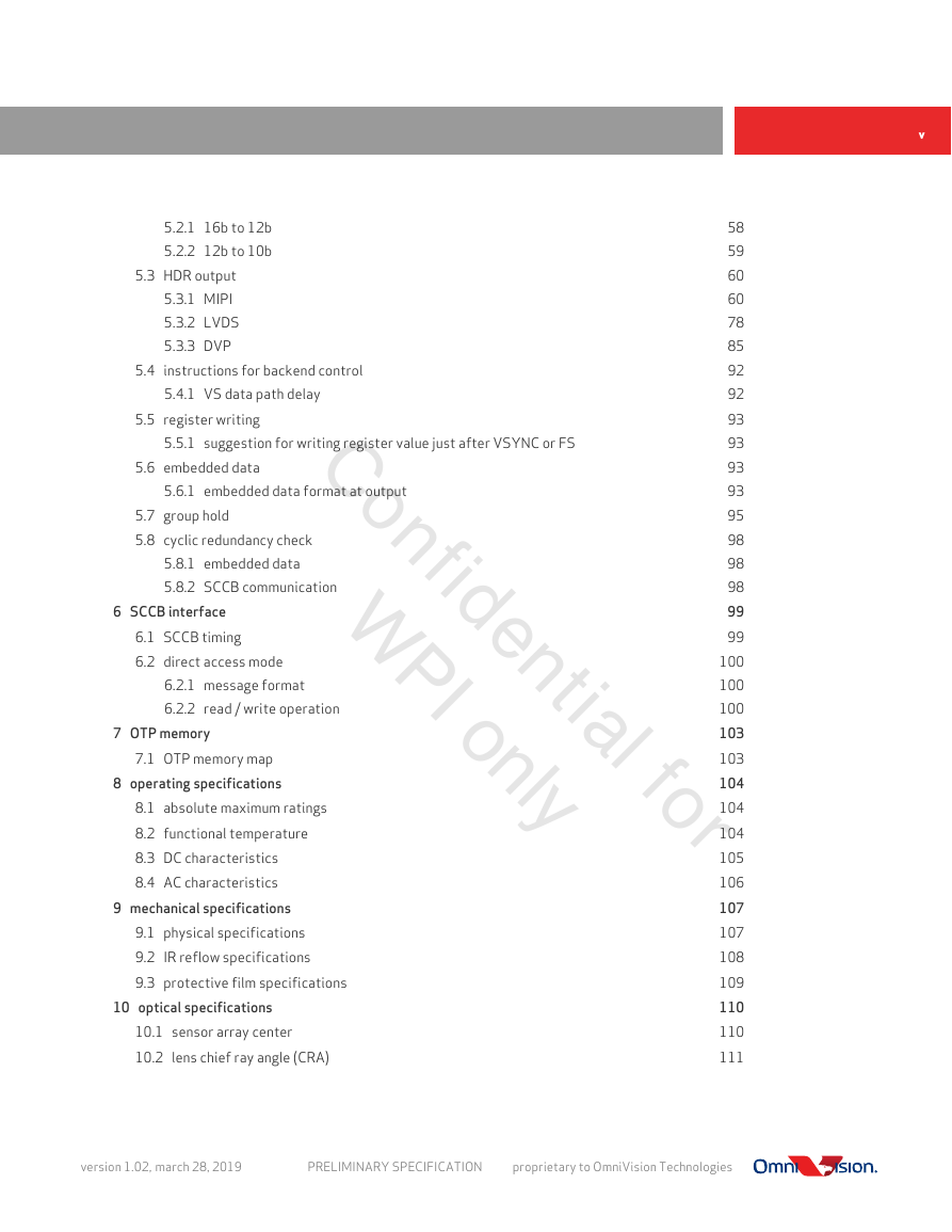
v 5.2.1 16b to 12b 5.2.2 12b to 10b 5.3 HDR output 5.3.1 MIPI 5.3.2 LVDS 5.3.3 DVP 5.4 instructions for backend control 5.4.1 VS data path delay 5.5 register writing 5.5.1 suggestion for writing register value just after VSYNC or FS 5.6 embedded data 5.6.1 embedded data format at output 5.7 group hold 5.8 cyclic redundancy check 5.8.1 embedded data 5.8.2 SCCB communication 6 SCCB interface 6.1 SCCB timing 6.2 direct access mode 6.2.1 message format 6.2.2 read / write operation 7 OTP memory 7.1 OTP memory map 8 operating specifications 8.1 absolute maximum ratings 8.2 functional temperature 8.3 DC characteristics 8.4 AC characteristics 9 mechanical specifications 9.1 physical specifications 9.2 IR reflow specifications 9.3 protective film specifications 10 optical specifications 10.1 sensor array center 10.2 lens chief ray angle (CRA) 58 59 60 60 78 85 92 92 93 93 93 93 95 98 98 98 99 99 100 100 100 103 103 104 104 104 105 106 107 107 108 109 110 110 111 version 1.02, march 28, 2019 PRELIMINARY SPECIFICATION proprietary to OmniVision Technologies Confidential forWPI onlyPowered by TCPDF (www.tcpdf.org)
RGB-Ir CMOS 1080p (1920x1080) high dynamic range (HDR) high definition image sensor OV2778 appendix A register table A.1 module name and address range A.2 device control registers 113 113 114 version 1.02, march 28, 2019 PRELIMINARY SPECIFICATION proprietary to OmniVision Technologies Confidential forWPI onlyPowered by TCPDF (www.tcpdf.org)
00list of figures vii standalone camera block diagram for automotive applications figure 1-1 multi-camera block diagram figure 1-2 pin diagram figure 1-3 OV2778 MIPI reference schematic figure 1-4 OV2778 DVP reference schematic figure 1-5 OV2778 power supplies and recommended external decoupling figure 1-6 power on timing diagram figure 1-7 OV2778 block diagram figure 2-1 sensor core block diagram figure 3-1 pixel array region RGB-Ir filter layout figure 3-2 exposures and captures diagram figure 3-3 integration time diagram figure 3-4 pixel array access diagram figure 3-5 horizontal mirror and vertical flip samples figure 3-6 row address versus time graph figure 3-7 frame output timing diagram figure 3-8 figure 3-9 PLL1 control diagram figure 3-10 PLL2 control diagram figure 4-1 figure 4-2 figure 4-3 figure 4-4 figure 4-5 figure 4-6 figure 4-7 figure 4-8 figure 4-9 figure 4-10 black and white squares test pattern figure 4-11 chart test pattern figure 4-12 HDR combine principle diagram figure 5-1 figure 5-2 image processor block diagram color bar types vertical bars test pattern vertical bars with vertical gradient test pattern vertical bars with horizontal gradient test pattern vertical bars with diagonal gradient test pattern vertical bars with rolling line test pattern random image test pattern color squares test pattern 16-bit to 12-bit PWL compression 12-bit to 10-bit PWL compression 12 13 14 21 22 23 24 27 29 30 30 31 32 33 34 35 46 46 49 50 51 51 51 51 52 52 52 52 53 54 58 59 version 1.02, march 28, 2019 PRELIMINARY SPECIFICATION proprietary to OmniVision Technologies Confidential forWPI onlyPowered by TCPDF (www.tcpdf.org)
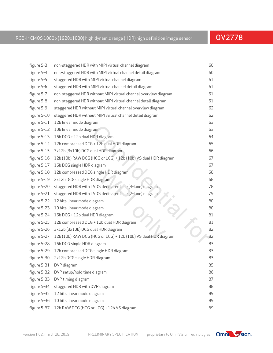
RGB-Ir CMOS 1080p (1920x1080) high dynamic range (HDR) high definition image sensor OV2778 non-staggered HDR with MIPI virtual channel diagram non-staggered HDR with MIPI virtual channel detail diagram staggered HDR with MIPI virtual channel diagram staggered HDR with MIPI virtual channel detail diagram non-staggered HDR without MIPI virtual channel overview diagram non-staggered HDR without MIPI virtual channel detail diagram staggered HDR without MIPI virtual channel overview diagram figure 5-3 figure 5-4 figure 5-5 figure 5-6 figure 5-7 figure 5-8 figure 5-9 figure 5-10 staggered HDR without MIPI virtual channel detail diagram figure 5-11 12b linear mode diagram figure 5-12 10b linear mode diagram figure 5-13 16b DCG + 12b dual HDR diagram figure 5-14 12b compressed DCG + 12b dual HDR diagram figure 5-15 3x12b (3x10b) DCG dual HDR diagram figure 5-16 12b (10b) RAW DCG (HCG or LCG) + 12b (10b) VS dual HDR diagram figure 5-17 16b DCG single HDR diagram figure 5-18 12b compressed DCG single HDR diagram figure 5-19 2x12b DCG single HDR diagram figure 5-20 staggered HDR with LVDS dedicated lane (4-lane) diagram figure 5-21 staggered HDR with LVDS dedicated lane (2-lane) diagram figure 5-22 12 bits linear mode diagram figure 5-23 10 bits linear mode diagram figure 5-24 16b DCG + 12b dual HDR diagram figure 5-25 12b compressed DCG + 12b dual HDR diagram figure 5-26 3x12b (3x10b) DCG dual HDR diagram figure 5-27 12b (10b) RAW DCG (HCG or LCG) + 12b (10b) VS dual HDR diagram figure 5-28 16b DCG single HDR diagram figure 5-29 12b compressed DCG single HDR diagram figure 5-30 2x12b DCG single HDR diagram figure 5-31 DVP diagram figure 5-32 DVP setup/hold time diagram figure 5-33 DVP timing diagram figure 5-34 staggered HDR with DVP diagram figure 5-35 12 bits linear mode diagram figure 5-36 10 bits linear mode diagram figure 5-37 12b RAW DCG (HCG or LCG) + 12b VS diagram 60 60 61 61 61 61 62 62 63 63 64 65 66 67 67 68 68 78 79 80 80 81 81 82 82 83 83 83 85 86 87 88 89 89 89 version 1.02, march 28, 2019 PRELIMINARY SPECIFICATION proprietary to OmniVision Technologies Confidential forWPI onlyPowered by TCPDF (www.tcpdf.org)
分享到:
收藏