SPI 协议 2008-08-11 19:57
The Serial Peripheral Interface Bus or SPI (often pronounced "es-pē-ī" [IPA: ɛs pi: 'aɪ] or "spy"
[IPA: spaɪ]) bus is a synchronous serial data link standard named by Motorola that operates in full
duplex mode. Devices communicate in master/slave mode where the master device initiates the
data frame. Multiple slave devices are allowed with individual slave select (chip select) lines.
Sometimes SPI is called a "four wire" serial bus, contrasting with three, two, and one wire serial
buse
spi 协议是一种同步的串行数据连接标准,由摩托罗拉公司命名,可工作与全双工方式。
相关通讯设备可工作与 m/s 模式。主设备发起数据帧,允许多个从设备的存在。每个重设备
有独立的片选信号。SPI 一般来说是四线串行总线结构,不同于三线两线或者一线的串行总
线。
interface 接口:
The SPI bus specifies four logic signals. 定义四个信号逻辑
SCLK — Serial Clock (output from master) 时钟(主设备发出)
MOSI/SIMO — Master Output, Slave Input (output from master)数据信号线 mosi(主设备发
出)
MISO/SOMI — Master Input, Slave Output (output from slave) 数据信号线(从设备)
SS — Slave Select (active low; output from master) 片选信号
Alternative naming conventions are also widely used:可选择的其他常用命名方式
SCK, CLK — Serial Clock (output from master)
SDI, DI, SI — Serial Data In
SDO, DO, SO — Serial Data Out
nCS, CS, nSS, STE — Chip Select, Slave Transmit Enable (active low; output from master)
The SDI/SDO (DI/DO, SI/SO) convention requires that SDO on the master be connected to SDI
on the slave, and vice-versa.
SPI port pin names for particular IC products may differ from those depicted in these illustrations.
spi 的 ic 产品中 i 端口管脚命名可能同上面不一样。
Operation 操作
The SPI bus can operate with a single master device and with one or more slave devices.
spi 总线可以操作与一个主设备多个从设备的模式
If a single slave device is used, the SS pin may be fixed to logic low if the slave permits it. Some
slaves require the falling edge (high->low transition) of the slave select to initiate an action such
as the MAX1242 by Maxim, an ADC, that starts conversion on said transition. With multiple slave
devices, an independent SS signal is required from the master for each slave device.
�
如果需要使用某个从设备,相应的 ss 管脚的电压将被拉低。有些从设备需要下降沿来选择
从设备以启动一个动作。如果是多个从设备,那么需要多个片选信号线。
Data Transmission 数据传送
To begin a communication, the master first configures the clock, using a frequency less than or
equal to the maximum frequency the slave device supports. Such frequencies are commonly in the
range of 1-70 MHz.。首先确定时钟频率
The master then pulls the slave select low for the desired chip. If a waiting period is required (such
as for analog-to-digital conversion) then the master must wait for at least that period of time
before starting to issue clock cycles.然后使相应从设备的片选信号有效(低电平有效)
During each SPI clock cycle, a full duplex data transmission occurs:在每一个 spi 时钟周期,发生
一个全双工的数据传送。
the master sends a bit on the MOSI line; the slave reads it from that same line
主设备在 mosi 线上发送一位数据,从设备在此线同时接受一位数据
the slave sends a bit on the MISO line; the master reads it from that same line
从设备在 miso 线上发送一位数据,主设备在此线上接受该数据。
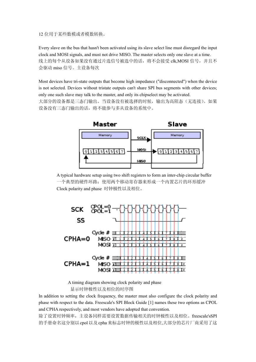
大概来说来说如下图呈环形数据传输。
Not all transmissions require all four of these operations to be meaningful but they do happen.
当然虽然这四个操作每次都会发生,但是这四个操作并不是对所有的传输都有用。
Transmissions normally involve two shift registers of some given word size, such as eight bits,
one in the master and one in the slave; they are connected in a ring. Data is usually shifted out
with the most significant bit first, while shifting a new least significant bit into the same register.
After that register has been shifted out, the master and slave have exchanged register values. Then
each device takes that value and does something with it, such as writing it to memory. If there is
more data to exchange, the shift registers are loaded with new data and the process repeats.
传输过程中包括一对移位寄存器,主设备一个,从设备一个,两个寄存器是以环形头尾相连。
传输结束之后两移位寄存器的数据互相交换。如果需要传输其他的数据,移位寄存器将下载
新的数据并继续发生移位的操作。
Transmissions may involve any number of clock cycles. When there are no more data to be
transmitted, the master stops toggling its clock. Normally, it then deselects the slave.
传输过程需要多个时钟周期。当不再需要传输数据时,主设备将停止时钟的切换,通常并且
使从设备的片选信号失效。
Transmissions often consist of 8-bit words, and a master can initiate multiple such transmissions if
it wishes/needs. However, other word sizes are also common, such as 16-bit words for touchscreen
controllers or audio codecs, like the TSC2101 from Texas Instruments; or 12-bit words for many
digital-to-analog or analog-to-digital converters.
每帧的传输位数一般为 8 ,12,16 等位数。比如说 TI 公司的某些器件,这些器件通常为
�
12 位用于某些数模或者模数转换。
Every slave on the bus that hasn't been activated using its slave select line must disregard the input
clock and MOSI signals, and must not drive MISO. The master selects only one slave at a time.
线上的每个从设备如果没有通过片选信号被选中的话,将不会接受 clk,MOSI 信号,并且不
会驱动 miso 信号。主设备每次
Most devices have tri-state outputs that become high impedance ("disconnected") when the device
is not selected. Devices without tristate outputs can't share SPI bus segments with other devices;
only one such slave may talk to the master, and only its chipselect may be activated.
大部分的设备都是三态门输出。当设备没有被选择的时候,输出为高阻态(无连接)。如果
设备没有三态门输出的话,将不能参与多从设备的系统中。
A typical hardware setup using two shift registers to form an inter-chip circular buffer
一个典型的硬件环路:使用两个移动寄存器来形成一个内置芯片的环形缓冲
Clock polarity and phase 时钟极性以及相位。
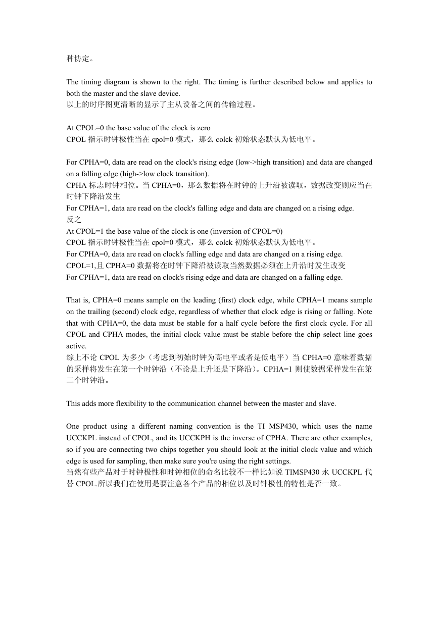
A timing diagram showing clock polarity and phase
显示时钟极性以及相位的时序图
In addition to setting the clock frequency, the master must also configure the clock polarity and
phase with respect to the data. Freescale's SPI Block Guide [1] names these two options as CPOL
and CPHA respectively, and most vendors have adopted that convention.
除了设置时钟频率,主设备同样需要设置数据传输相关的时钟极性以及相位。freescale'sSPI
的手册命名这分别以 cpol 以及 cpha 来标志时钟的极性以及相位,大部分的芯片厂商采用了这
�
种协定。
The timing diagram is shown to the right. The timing is further described below and applies to
both the master and the slave device.
以上的时序图更清晰的显示了主从设备之间的传输过程。
At CPOL=0 the base value of the clock is zero
CPOL 指示时钟极性当在 cpol=0 模式,那么 colck 初始状态默认为低电平。
For CPHA=0, data are read on the clock's rising edge (low->high transition) and data are changed
on a falling edge (high->low clock transition).
CPHA 标志时钟相位。当 CPHA=0,那么数据将在时钟的上升沿被读取,数据改变则应当在
时钟下降沿发生
For CPHA=1, data are read on the clock's falling edge and data are changed on a rising edge.
反之
At CPOL=1 the base value of the clock is one (inversion of CPOL=0)
CPOL 指示时钟极性当在 cpol=0 模式,那么 colck 初始状态默认为低电平。
For CPHA=0, data are read on clock's falling edge and data are changed on a rising edge.
CPOL=1,且 CPHA=0 数据将在时钟下降沿被读取当然数据必须在上升沿时发生改变
For CPHA=1, data are read on clock's rising edge and data are changed on a falling edge.
That is, CPHA=0 means sample on the leading (first) clock edge, while CPHA=1 means sample
on the trailing (second) clock edge, regardless of whether that clock edge is rising or falling. Note
that with CPHA=0, the data must be stable for a half cycle before the first clock cycle. For all
CPOL and CPHA modes, the initial clock value must be stable before the chip select line goes
active.
综上不论 CPOL 为多少(考虑到初始时钟为高电平或者是低电平)当 CPHA=0 意味着数据
的采样将发生在第一个时钟沿(不论是上升还是下降沿)。CPHA=1 则使数据采样发生在第
二个时钟沿。
This adds more flexibility to the communication channel between the master and slave.
One product using a different naming convention is the TI MSP430, which uses the name
UCCKPL instead of CPOL, and its UCCKPH is the inverse of CPHA. There are other examples,
so if you are connecting two chips together you should look at the initial clock value and which
edge is used for sampling, then make sure you're using the right settings.
当然有些产品对于时钟极性和时钟相位的命名比较不一样比如说 TIMSP430 永 UCCKPL 代
替 CPOL.所以我们在使用是要注意各个产品的相位以及时钟极性的特性是否一致。
�


 2023年江西萍乡中考道德与法治真题及答案.doc
 2012年重庆南川中考生物真题及答案.doc
 2013年江西师范大学地理学综合及文艺理论基础考研真题.doc
 2020年四川甘孜小升初语文真题及答案I卷.doc
 2020年注册岩土工程师专业基础考试真题及答案.doc
 2023-2024学年福建省厦门市九年级上学期数学月考试题及答案.doc
 2021-2022学年辽宁省沈阳市大东区九年级上学期语文期末试题及答案.doc
 2022-2023学年北京东城区初三第一学期物理期末试卷及答案.doc
 2018上半年江西教师资格初中地理学科知识与教学能力真题及答案.doc
 2012年河北国家公务员申论考试真题及答案-省级.doc
 2020-2021学年江苏省扬州市江都区邵樊片九年级上学期数学第一次质量检测试题及答案.doc
 2022下半年黑龙江教师资格证中学综合素质真题及答案.doc