Fremont Micro Devices FT24C02A
Two-Wire Serial EEPROM
2K (8-bit wide)
Tel: 0755-83264115
Fax:0755-83955172
URL: http://w.ww.qsdaz.com
FEATURES
Low voltage and low power operations:
FT24C02A: VCC = 1.8V to 5.5V, Industrial temperature range (-40℃ to 85℃).
Two Versions of FT24C02A:
FT24C02A-5xx: Low cost with 5 valid pins. Suitable for most application except those with
more than one EEPROM on the same IIC Bus. Details in the “Device Addressing” section.
FT24C02A-Uxx: 8 valid pins suitable for all application.
Maximum Standby current < 1µA (typically 0.02µA and 0.06µA @ 1.8V and 5.5V respectively).
16 bytes page write mode.
Partial page write operation allowed.
Internally organized: 256 × 8 (2K).
Standard 2-wire bi-directional serial interface.
Schmitt trigger, filtered inputs for noise protection.
Self-timed programming cycle (5ms maximum).
1 MHz (5V), 400 kHz (1.8V, 2.5V, 2.7V) Compatibility.
Automatic erase before write operation.
Write protect pin for hardware data protection.
High reliability: typically 1, 000,000 cycles endurance.
100 years data retention.
Standard 8-pin PDIP/SOIC/TSSOP/DFN and 5-pin SOT-23/TSOT-23 Pb-free packages.
DESCRIPTION
The FT24C02A is 2048 bits of serial Electrical Erasable and Programmable Read Only Memory,
commonly known as EEPROM. They are organized as 256 words of 8 bits (1 byte) each. The devices
are fabricated with proprietary advanced CMOS process for low power and low voltage applications.
These devices are available in standard 8-lead PDIP, 8-lead JEDEC SOIC, 8-lead TSSOP, 8-lead DFN
and 5-lead SOT-23/TSOT-23 packages. A standard 2-wire serial interface is used to address all read
and write functions. Our extended VCC range (1.8V to 5.5V) devices enables wide spectrum of
applications.
© 2009 Fremont Micro Devices Inc. DS3011B-page1
�
FT24C02A
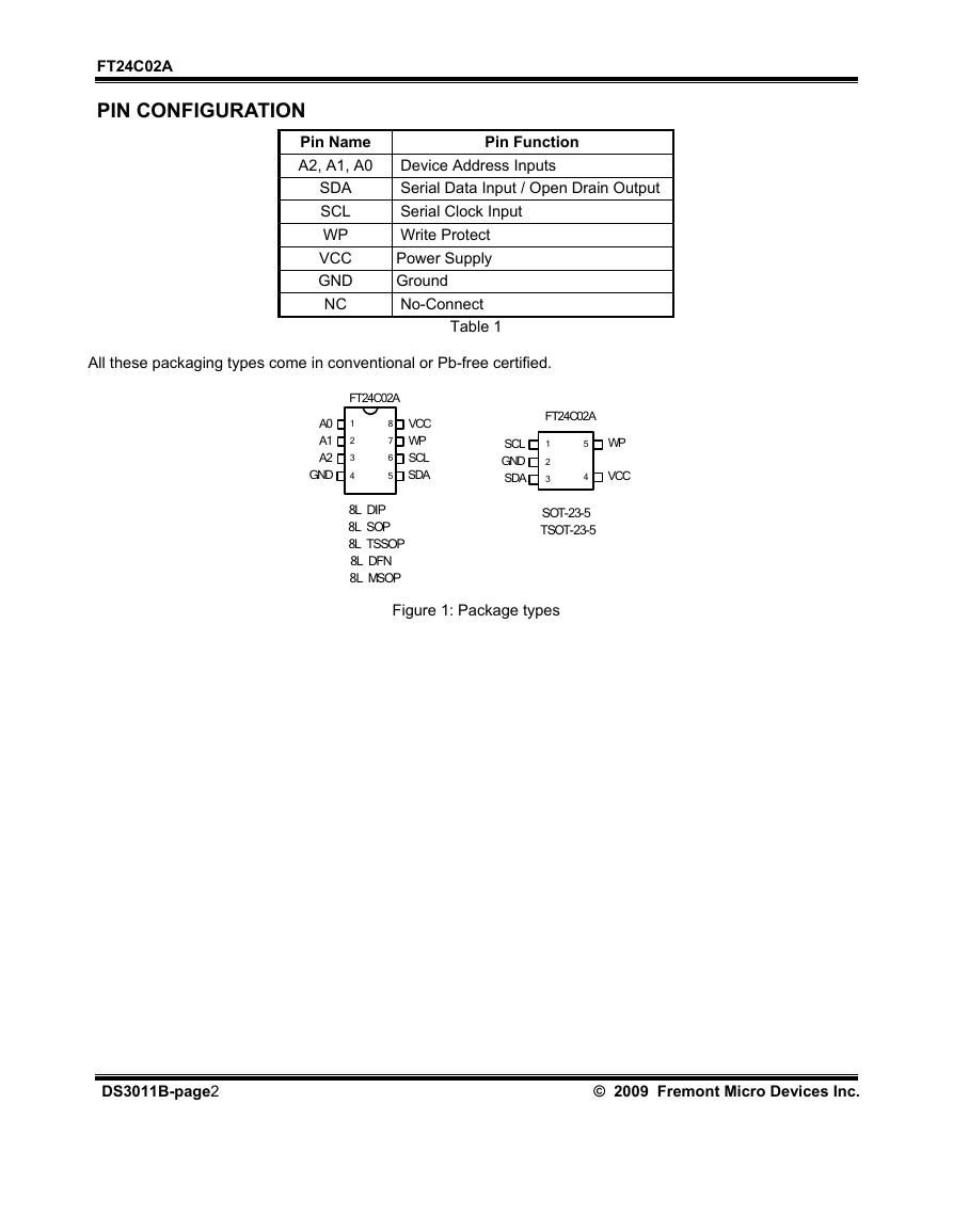
PIN CONFIGURATION
Pin Name
A2, A1, A0
SDA
SCL
WP
VCC
GND
NC
Pin Function
Device Address Inputs
Serial Data Input / Open Drain Output
Serial Clock Input
Write Protect
Power Supply
Ground
No-Connect
All these packaging types come in conventional or Pb-free certified.
Table 1
FT24C02A
A0
A1
A2
GND
1
2
3
4
8
7
6
5
VCC
WP
SCL
SDA
8L DIP
8L SOP
8L TSSOP
8L DFN
8L MSOP
FT24C02A
SCL
GND
SDA
1
2
3
5
4
WP
VCC
SOT-23-5
TSOT-23-5
Figure 1: Package types
DS3011B-page2 © 2009 Fremont Micro Devices Inc.
�
ABSOLUTE MAXIMUM RATINGS
FT24C02A
Industrial operating temperature:
Storage temperature:
Input voltage on any pin relative to ground:
Maximum voltage:
ESD protection on all pins: >2000V
* Stresses exceed those listed under “Absolute Maximum Rating” may cause permanent damage to the
device. Functional operation of the device at conditions beyond those listed in the specification is not
guaranteed. Prolonged exposure to extreme conditions may affect device reliability or functionality.
-40℃ to 85℃
-50℃ to 125℃
-0.3V to VCC + 0.3V
8V
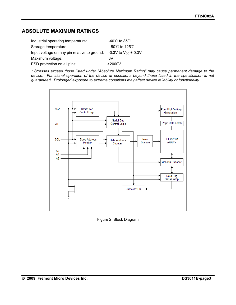
Figure 2: Block Diagram
© 2009 Fremont Micro Devices Inc. DS3011B-page3
�
FT24C02A
PIN DESCRIPTIONS
(A) SERIAL CLOCK (SCL)
The rising edge of this SCL input is to latch data into the EEPROM device while the falling edge of
this clock is to clock data out of the EEPROM device.
(B) SERIAL DATA LINE (SDA)
SDA data line is a bi-directional signal for the serial devices. It is an open drain output signal and can
be wired-OR with other open-drain output devices.
(C) WRITE PROTECT (WP)
The FT24C02A devices have a WP pin to protect the whole EEPROM array from programming.
Programming operations are allowed if WP pin is left un-connected or input to VIL. Conversely all
programming functions are disabled if WP pin is connected to VIH or VCC. Read operations is not
affected by the WP pin’s input level.
MEMORY ORGANIZATION
The FT24C02A devices have 16 pages. Since each page has 16 bytes, random word addressing to
FT24C02A will require 8 bits data word addresses.
DEVICE OPERATION
(A) SERIAL CLOCK AND DATA TRANSITIONS
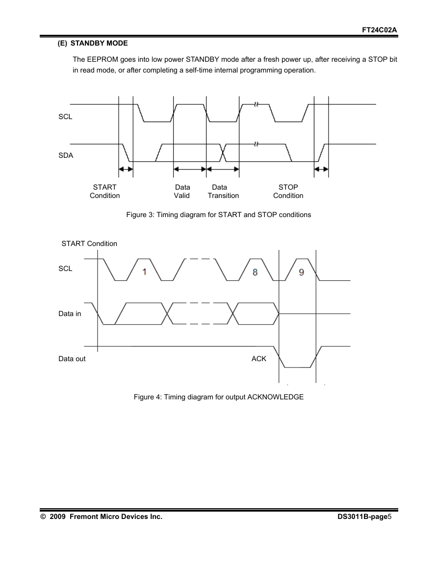
The SDA pin is typically pulled to high by an external resistor. Data is allowed to change only when
Serial clock SCL is at VIL. Any SDA signal transition may interpret as either a START or STOP
condition as described below.
(B) START CONDITION
With SCL ≥ VIH, a SDA transition from high to low is interpreted as a START condition. All valid
commands must begin with a START condition.
(C) STOP CONDITION
With SCL ≥ VIH, a SDA transition from low to high is interpreted as a STOP condition. All valid read
or write commands end with a STOP condition. The device goes into the STANDBY mode if it is after
a read command. A STOP condition after page or byte write command will trigger the chip into the
STANDBY mode after the self-timed internal programming finish.
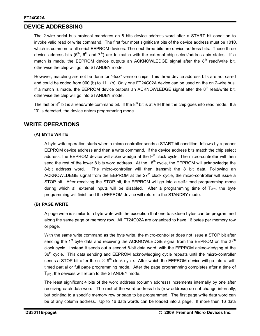
(D) ACKNOWLEDGE
The 2-wire protocol transmits address and data to and from the EEPROM in 8 bit words. The
EEPROM acknowledges the data or address by outputting a "0" after receiving each word. The
ACKNOWLEDGE signal occurs on the 9th serial clock after each word.
DS3011B-page4 © 2009 Fremont Micro Devices Inc.
�
(E) STANDBY MODE
The EEPROM goes into low power STANDBY mode after a fresh power up, after receiving a STOP bit
in read mode, or after completing a self-time internal programming operation.
FT24C02A
SCL
SDA
START
Condition
Data Data
Valid Transition
STOP
Condition
Figure 3: Timing diagram for START and STOP conditions
START Condition
SCL
Data in
Data out
ACK
Figure 4: Timing diagram for output ACKNOWLEDGE
© 2009 Fremont Micro Devices Inc. DS3011B-page5
�
FT24C02A
DEVICE ADDRESSING
The 2-wire serial bus protocol mandates an 8 bits device address word after a START bit condition to
invoke valid read or write command. The first four most significant bits of the device address must be 1010,
which is common to all serial EEPROM devices. The next three bits are device address bits. These three
device address bits (5th, 6th and 7th) are to match with the external chip select/address pin states. If a
match is made, the EEPROM device outputs an ACKNOWLEDGE signal after the 8th read/write bit,
otherwise the chip will go into STANDBY mode.
However, matching are not be done for “-5xx” version chips. This three device address bits are not cared
and could be coded from 000 (b) to 111 (b). Only one FT24C02A device can be used on the on 2-wire bus.
If a match is made, the EEPROM device outputs an ACKNOWLEDGE signal after the 8th read/write bit,
otherwise the chip will go into STANDBY mode.
The last or 8th bit is a read/write command bit. If the 8th bit is at VIH then the chip goes into read mode. If a
“0” is detected, the device enters programming mode.
WRITE OPERATIONS
(A) BYTE WRITE
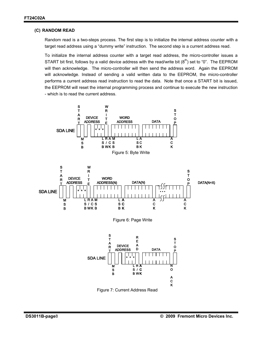
A byte write operation starts when a micro-controller sends a START bit condition, follows by a proper
EEPROM device address and then a write command. If the device address bits match the chip select
address, the EEPROM device will acknowledge at the 9th clock cycle. The micro-controller will then
send the rest of the lower 8 bits word address. At the 18th cycle, the EEPROM will acknowledge the
8-bit address word. The micro-controller will then transmit the 8 bit data. Following an
ACKNOWLDEGE signal from the EEPROM at the 27th clock cycle, the micro-controller will issue a
STOP bit. After receiving the STOP bit, the EEPROM will go into a self-timed programming mode
during which all external inputs will be disabled. After a programming time of TWC, the byte
programming will finish and the EEPROM device will return to the STANDBY mode.
(B) PAGE WRITE
A page write is similar to a byte write with the exception that one to sixteen bytes can be programmed
along the same page or memory row. All FT24C02A are organized to have 16 bytes per memory row
or page.
With the same write command as the byte write, the micro-controller does not issue a STOP bit after
sending the 1st byte data and receiving the ACKNOWLEDGE signal from the EEPROM on the 27th
clock cycle. Instead it sends out a second 8-bit data word, with the EEPROM acknowledging at the
36th cycle. This data sending and EEPROM acknowledging cycle repeats until the micro-controller
sends a STOP bit after the n × 9th clock cycle. After which the EEPROM device will go into a self-
timed partial or full page programming mode. After the page programming completes after a time of
TWC, the devices will return to the STANDBY mode.
The least significant 4 bits of the word address (column address) increments internally by one after
receiving each data word. The rest of the word address bits (row address) do not change internally,
but pointing to a specific memory row or page to be programmed. The first page write data word can
be of any column address. Up to 16 data words can be loaded into a page. If more then 16 data
DS3011B-page6 © 2009 Fremont Micro Devices Inc.
�
words are loaded, the 17th data word will be loaded to the 1st data word column address. The 18th
data word will be loaded to the 2nd data word column address and so on. In other word, data word
address (column address) will “roll” over the previously loaded data.
FT24C02A
(C) ACKNOWLEDGE POLLING
ACKNOWLEDGE polling may be used to poll the programming status during a self-timed internal
programming. By issuing a valid read or write address command, the EEPROM will not acknowledge
at the 9th clock cycle if the device is still in the self-timed programming mode. However, if the
programming completes and the chip has returned to the STANDBY mode, the device will return a
valid ACKNOWLEDGE signal at the 9th clock cycle.
READ OPERATIONS
The read command is similar to the write command except the 8th read/write bit in address word is set to “1”.
The three read operation modes are described as follows:
(A) CURRENT ADDRESS READ
The EEPROM internal address word counter maintains the last read or write address plus one if the
power supply to the device has not been cut off. To initiate a current address read operation, the
micro-controller issues a START bit and a valid device address word with the read/write bit (8th) set to
“1”. The EEPROM will response with an ACKNOWLEDGE signal on the 9th serial clock cycle. An 8-
bit data word will then be serially clocked out. The internal address word counter will then
automatically increase by one. For current address read the micro-controller will not issue an
ACKNOWLEDGE signal on the 18th clock cycle. The micro-controller issues a valid STOP bit after
the 18th clock cycle to terminate the read operation. The device then returns to STANDBY mode.
(B) SEQUENTIAL READ
The sequential read is very similar to current address read. The micro-controller issues a START bit
and a valid device address word with read/write bit (8th) set to “1”. The EEPROM will response with
an ACKNOWLEDGE signal on the 9th serial clock cycle. An 8-bit data word will then be serially
clocked out. Meanwhile the internally address word counter will then automatically increase by one.
Unlike current address read, the micro-controller sends an ACKNOWLEDGE signal on the 18th clock
cycle signaling the EEPROM device that it wants another byte of data. Upon receiving the
ACKNOWLEDGE signal, the EEPROM will serially clocked out an 8-bit data word based on the
incremented internal address counter. If the micro-controller needs another data, it sends out an
ACKNOWLEDGE signal on the 27th clock cycle. Another 8-bit data word will then be serially clocked
out. This sequential read continues as long as the micro-controller sends an ACKNOWLEDGE signal
after receiving a new data word. When the internal address counter reaches its maximum valid
address, it rolls over to the beginning of the memory array address. Similar to current address read,
the micro-controller can terminate the sequential read by not acknowledging the last data word
received, but sending a STOP bit afterwards instead.
© 2009 Fremont Micro Devices Inc. DS3011B-page7
�
FT24C02A
(C) RANDOM READ
Random read is a two-steps process. The first step is to initialize the internal address counter with a
target read address using a “dummy write” instruction. The second step is a current address read.
To initialize the internal address counter with a target read address, the micro-controller issues a
START bit first, follows by a valid device address with the read/write bit (8th) set to “0”. The EEPROM
will then acknowledge. The micro-controller will then send the address word. Again the EEPROM
will acknowledge. Instead of sending a valid written data to the EEPROM, the micro-controller
performs a current address read instruction to read the data. Note that once a START bit is issued,
the EEPROM will reset the internal programming process and continue to execute the new instruction
- which is to read the current address.
S
T
A
R
T
DEVICE
ADDRESS
W
R
I
T
E
SDA LINE
* * *
M
S
B
L
S
B
R
/
W
A
C
K
WORD
ADDRESS
DATA
M
S
B
Figure 5: Byte Write
A
C
K
L
S
B
S
T
A
R
T
DEVICE
ADDRESS
W
R
I
T
E
SDA LINE
* * *
M
S
B
L
S
B
R
/
W
M
S
B
A
C
K
WORD
ADDRESS(N)
DATA(N)
...
A
C
K
L
S
B
A
A
C
C
K
K
Figure 6: Page Write
S
T
A
R
T
R
E
A
D
DEVICE
ADDRESS
DATA
SDA LINE
* * *
M
S
B
L
S
B
R
/
W
A
A
C
C
K
K
Figure 7: Current Address Read
DATA(N+X)
S
T
O
P
A
C
K
S
T
O
P
A
C
K
S
T
O
P
N
O
A
C
K
DS3011B-page8 © 2009 Fremont Micro Devices Inc.
�



 2023年江西萍乡中考道德与法治真题及答案.doc
 2012年重庆南川中考生物真题及答案.doc
 2013年江西师范大学地理学综合及文艺理论基础考研真题.doc
 2020年四川甘孜小升初语文真题及答案I卷.doc
 2020年注册岩土工程师专业基础考试真题及答案.doc
 2023-2024学年福建省厦门市九年级上学期数学月考试题及答案.doc
 2021-2022学年辽宁省沈阳市大东区九年级上学期语文期末试题及答案.doc
 2022-2023学年北京东城区初三第一学期物理期末试卷及答案.doc
 2018上半年江西教师资格初中地理学科知识与教学能力真题及答案.doc
 2012年河北国家公务员申论考试真题及答案-省级.doc
 2020-2021学年江苏省扬州市江都区邵樊片九年级上学期数学第一次质量检测试题及答案.doc
 2022下半年黑龙江教师资格证中学综合素质真题及答案.doc