Application Note AN-978
HV Floating MOS-Gate Driver ICs
(HEXFET is a trademark of International Rectifier)
Table of Contents
Page
Gate drive requirement of high-side devices............................................................... 2
A typical block diagram ............................................................................................... 3
How to select the bootstrap components.................................................................... 5
How to calculate the power dissipation in an MGD..................................................... 6
How to deal with negative transients on the Vs pin ..................................................... 9
Layout and other general guidelines........................................................................... 11
How to boost gate drive current to drive modules....................................................... 14
How to provide a continuous gate drive...................................................................... 17
How to generate a negative gate bias......................................................................... 19
How to drive a buck converter..................................................................................... 22
Dual forward converter and switched reluctance motor drives ................................... 24
Full bridge with current mode control.......................................................................... 24
Brushless and induction motor drives ......................................................................... 26
Push-pull ..................................................................................................................... 27
High-side P-channel.................................................................................................... 27
Troubleshooting guidelines ......................................................................................... 28
www.irf.com
AN-978 RevD
1
�
1. GATE DRIVE REQUIREMENTS OF HIGH-SIDE DEVICES
The gate drive requirements for a power MOSFET or IGBT utilized as a high-side switch (the
drain is connected to the high voltage rail, as shown in Figure 1) driven in full enhancement (i.e.,
lowest voltage drop across its terminals) can be summarized as follows:
1. Gate voltage must be 10 V to 15 V higher than the source voltage. Being a high-side
switch, such gate voltage would have to be higher than the rail voltage, which is
frequently the highest voltage available in the system.
2. The gate voltage must be controllable from the logic, which is normally referenced to
ground. Thus, the control signals have to be level-shifted to the source of the high-
side power device, which, in most applications, swings between the two rails.
3. The power absorbed by the gate drive circuitry should not significantly affect the
overall efficiency.
V+
HIGH VOLTAGE RAIL
GATE
SOURCE
Figure 1: Power MOSFET in the High-Side Configuration
With these constraints in mind, several techniques are presently used to perform this function, as
shown in principle in Table I (see pg. 29). Each basic circuit can be implemented in a wide
variety of configurations.
International Rectifier’s family of MOS-gate drivers (MGDs) integrate most of the functions
required to drive one high-side and one low-side power MOSFET or IGBT in a compact, high
performance package. With the addition of few components, they provide very fast switching
speeds, as shown in Table II (see pg. 30) for the IRS2110, and low power dissipation. They can
operate on the bootstrap principle or with a floating power supply. Used in the bootstrap mode,
they can operate in most applications from frequencies in the tens of Hz up to hundreds of kHz.
www.irf.com
AN-978 RevD
2
�
2. TYPICAL BLOCK DIAGRAM
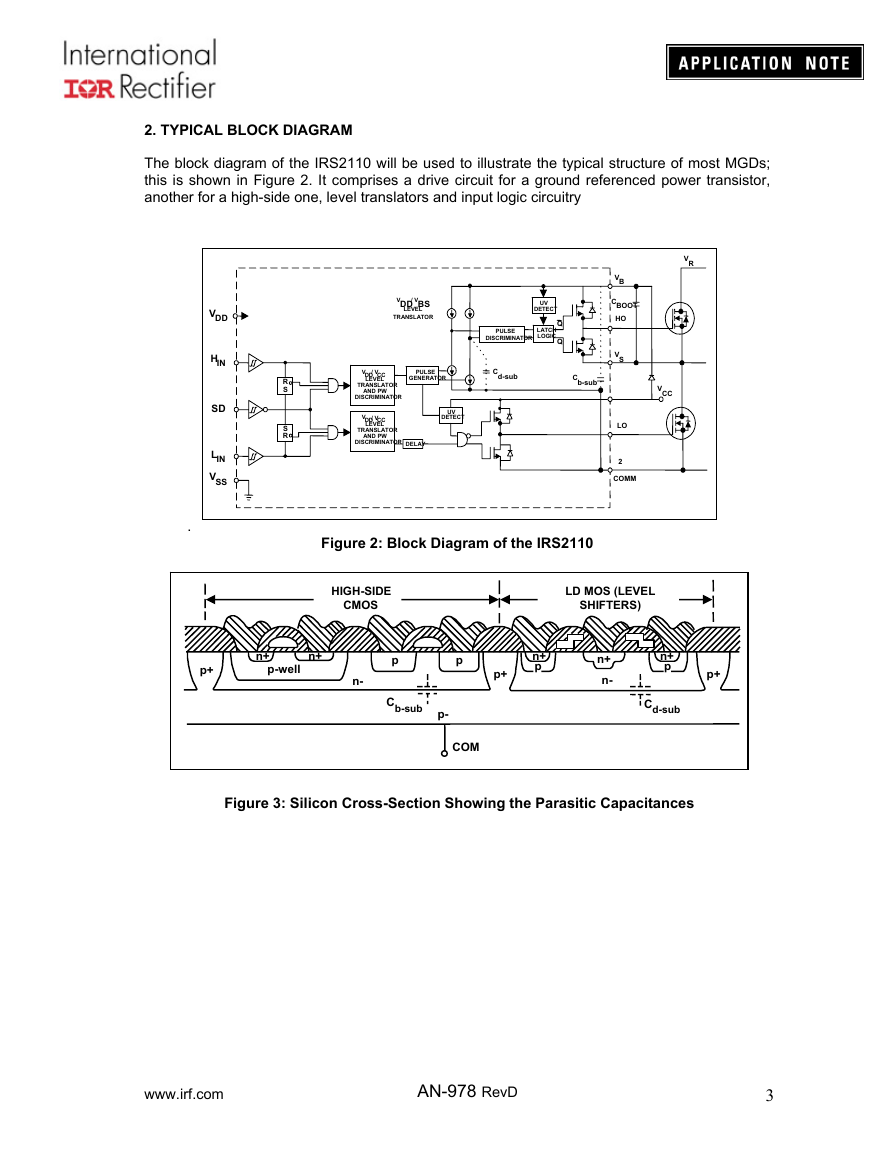
The block diagram of the IRS2110 will be used to illustrate the typical structure of most MGDs;
this is shown in Figure 2. It comprises a drive circuit for a ground referenced power transistor,
another for a high-side one, level translators and input logic circuitry
VDD
H IN
SD
L IN
V SS
.
VDD/ VBS
TRANSLATOR
LEVEL
UV
DETECT
PULSE
DISCRIMINATOR
LATCH
LOGIC
Q
Q
R S
R S
VDD/ VCC
LEVEL
TRANSLATOR
AND PW
DISCRIMINATOR
VDD/ VCC
LEVEL
TRANSLATOR
AND PW
DISCRIMINATOR
PULSE
GENERATOR
Cd-sub
Cb-sub
UV
DETECT
DELAY
V R
V CC
VB
CBOOT
HO
VS
LO
2
COMM
Figure 2: Block Diagram of the IRS2110
HIGH-SIDE
CMOS
LD MOS (LEVEL
SHIFTERS)
n+
p-well
n+
p+
n-
p
p
n+
p
p+
Cb-sub
p-
COM
n+
n-
n+ p
C d-sub
p+
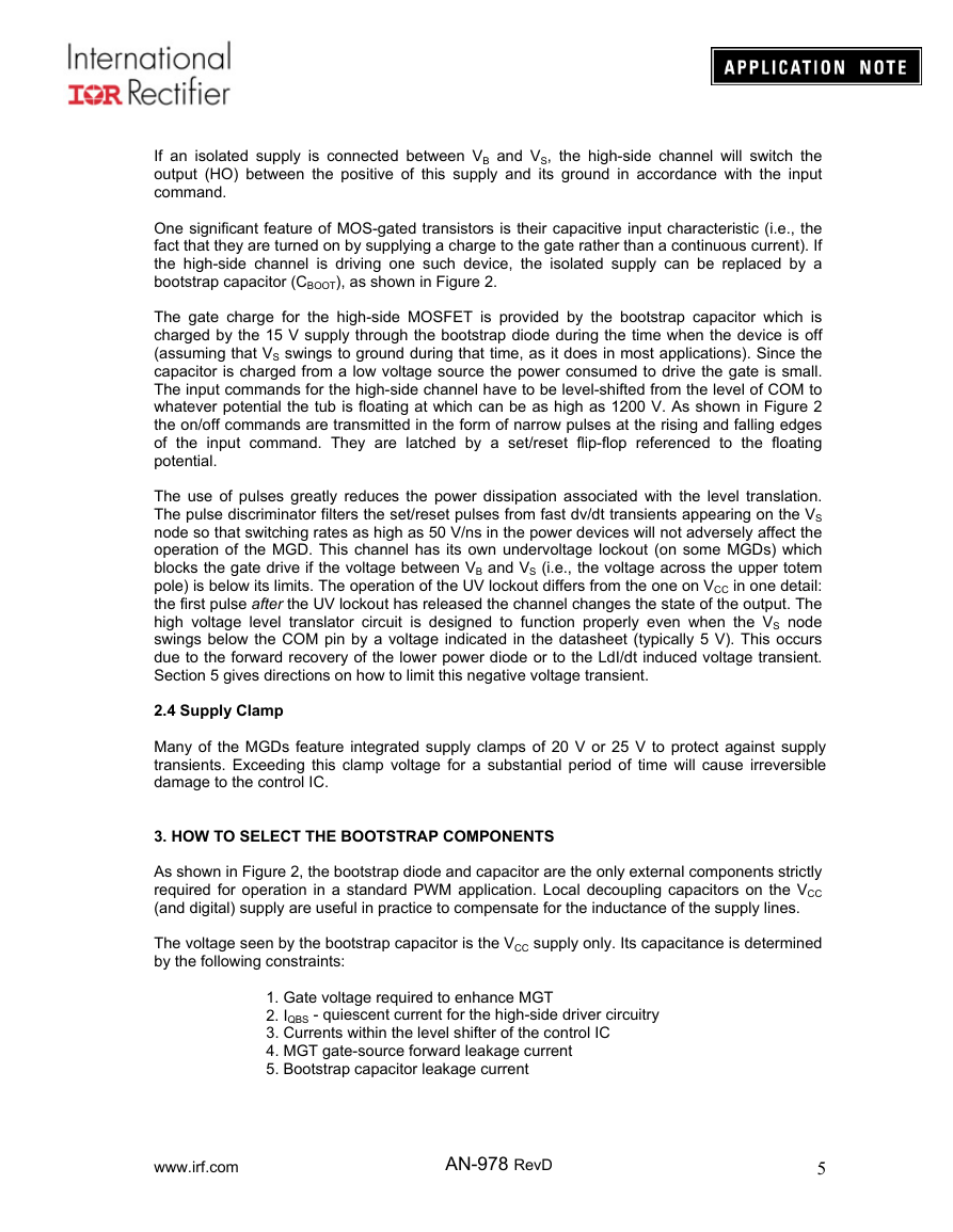
Figure 3: Silicon Cross-Section Showing the Parasitic Capacitances
www.irf.com
AN-978 RevD
3
�
2.1 Input Logic
Both channels are controlled by TTL/CMOS compatible inputs. The transition thresholds are
different from device to device. Some MGDs, (e.g., IRS211x) have the transition threshold
proportional to the logic supply VDD (3 to 20 V) and Schmitt trigger buffers with hysteresis equal
to 10% of VDD to accept inputs with long rise time. Other MGDs (e.g., IRS210x, IRS212x, and
IRS213x devices) have a fixed transition from logic 0 to logic 1 between 1.5 V to 2 V. Some
MGDs can drive only one high-side power device (e.g., IRS2117, IRS2127, and IRS21851).
Others can drive one high-side and one low-side power device. Others can drive a full three-
phase bridge (e.g., the IRS213x and IRS263x families). It goes without saying that any high-side
driver can also drive a low-side device. Those MGDs with two gate drive channel can have dual,
hence independent, input commands or a single input command with complementary drive and
predetermined deadtime.
Those applications that require a minimum deadtime should use MGDs with integrated deadtime
(half-bridge driver) or a high- and low-side driver in combination with passive components to
provide the needed deadtime, as shown in Section 12. Typically, the propagation delay between
input command and gate drive output is approximately the same for both channels at turn-on as
well as turn-off (with temperature dependence as characterized in the datasheet). For MGDs with
a positive high shutdown function (e.g., IRS2110), the outputs are shutdown internally, for the
remainder of the cycle, by a logic 1 signal at the shut down input.
The first input command after the removal of the shutdown signal clears the latch and activates
its channel. This latched shutdown lends itself to a simple implementation of a cycle-by-cycle
current control, as exemplified in Section 12. The signals from the input logic are coupled to the
individual channels through high noise immunity level translators. This allows the ground
reference of the logic supply (VSS) to swing by ±5 V with respect to the power ground (COM).
This feature is of great help in coping with the less than ideal ground layout of a typical power
conditioning circuit. As a further measure of noise immunity, a pulse-width discriminator screens
out pulses that are shorter than 50 ns or so.
2.2 Low-Side Channel
The driver’s output stage is implemented either with two n-channel MOSFETs in the totem pole
configuration (source follower as a current source and common source for current sinking), or
with an n-channel and a p-channel CMOS inverter stage. Each MOSFET can sink or source
gate currents from 0.12 A to 4 A, depending on the MGD. The source of the lower driver is
independently brought out to the COM pin so that a direct connection can be made to the source
of the power device for the return of the gate drive current. The relevance of this will be seen in
Section 5. An undervoltage lockout prevents either channel from operating if VCC is below the
specified value (typically 8.6/8.2 V).
Any pulse that is present at the input pin for the low-side channel when the UV lockout is
released turns on the power transistor from the moment the UV lockout is released. This
behavior is different from that of the high-side channel, as we will see in the next subsection.
2.3 High-Side Channel
This channel has been built into an “isolation tub” (Figure 3) capable of floating from 500 V or
1200 V to -5 V with respect to power ground (COM). The tub “floats” at the potential of VS.
Typically this pin is connected to the source of the high-side device, as shown in Figure 2 and
swings with it between the two rails.
www.irf.com
AN-978 RevD
4
�
If an isolated supply is connected between VB and VS, the high-side channel will switch the
output (HO) between the positive of this supply and its ground in accordance with the input
command.
One significant feature of MOS-gated transistors is their capacitive input characteristic (i.e., the
fact that they are turned on by supplying a charge to the gate rather than a continuous current). If
the high-side channel is driving one such device, the isolated supply can be replaced by a
bootstrap capacitor (CBOOT), as shown in Figure 2.
The gate charge for the high-side MOSFET is provided by the bootstrap capacitor which is
charged by the 15 V supply through the bootstrap diode during the time when the device is off
(assuming that VS swings to ground during that time, as it does in most applications). Since the
capacitor is charged from a low voltage source the power consumed to drive the gate is small.
The input commands for the high-side channel have to be level-shifted from the level of COM to
whatever potential the tub is floating at which can be as high as 1200 V. As shown in Figure 2
the on/off commands are transmitted in the form of narrow pulses at the rising and falling edges
of the input command. They are latched by a set/reset flip-flop referenced to the floating
potential.
The use of pulses greatly reduces the power dissipation associated with the level translation.
The pulse discriminator filters the set/reset pulses from fast dv/dt transients appearing on the VS
node so that switching rates as high as 50 V/ns in the power devices will not adversely affect the
operation of the MGD. This channel has its own undervoltage lockout (on some MGDs) which
blocks the gate drive if the voltage between VB and VS (i.e., the voltage across the upper totem
pole) is below its limits. The operation of the UV lockout differs from the one on VCC in one detail:
the first pulse after the UV lockout has released the channel changes the state of the output. The
high voltage level translator circuit is designed to function properly even when the VS node
swings below the COM pin by a voltage indicated in the datasheet (typically 5 V). This occurs
due to the forward recovery of the lower power diode or to the LdI/dt induced voltage transient.
Section 5 gives directions on how to limit this negative voltage transient.
2.4 Supply Clamp
Many of the MGDs feature integrated supply clamps of 20 V or 25 V to protect against supply
transients. Exceeding this clamp voltage for a substantial period of time will cause irreversible
damage to the control IC.
3. HOW TO SELECT THE BOOTSTRAP COMPONENTS
As shown in Figure 2, the bootstrap diode and capacitor are the only external components strictly
required for operation in a standard PWM application. Local decoupling capacitors on the VCC
(and digital) supply are useful in practice to compensate for the inductance of the supply lines.
The voltage seen by the bootstrap capacitor is the VCC supply only. Its capacitance is determined
by the following constraints:
1. Gate voltage required to enhance MGT
2. IQBS - quiescent current for the high-side driver circuitry
3. Currents within the level shifter of the control IC
4. MGT gate-source forward leakage current
5. Bootstrap capacitor leakage current
www.irf.com
AN-978 RevD
5
�
Factor 5 is only relevant if the bootstrap capacitor is an electrolytic capacitor, and can be ignored
if other types of capacitor are used. Therefore it is always better to use a non-electrolytic
capacitor if possible. For more detailed information on bootstrap component selection see DT98-
2a “Bootstrap Component Selection for Control IC’s.”
The minimum bootstrap capacitor value can be calculated from the following equation:
⎡
2 2
⎢
⎣
C
≥
g
Q I
+
V
qbs
(max)
f
cc
−
Q I
+
ls
+
V V
f
−
LS
)
⎤
⎥
⎦
Cbs leak
(
f
−VMin
where:
Qg = Gate charge of high-side FET
f = frequency of operation
ICbs (leak) = bootstrap capacitor leakage current
Iqbs (max) = Maximum VBS quiescent current
VCC = Logic section voltage source
Vf = Forward voltage drop across the bootstrap diode
VLS = Voltage drop across the low-side FET or load
VMin = Minimum voltage between VB and VS.
Qls = level shift charge required per cycle (typically 5 nC for 500 V/600 V MGDs and 20 nC for
1200 V MGDs)
The bootstrap diode must be able to block the full voltage seen in the specific circuit; in the
circuits of Figures 25, 28 and 29 this occurs when the top device is on and is about equal to the
voltage across the power rail. The current rating of the diode is the product of gate charge times
switching frequency. For an IRF450 HEXFET power MOSFET operating at 100 kHz it is
approximately 12 mA.
The high temperature reverse leakage characteristic of this diode can be an important parameter
in those applications where the capacitor has to hold the charge for a prolonged period of time.
For the same reason it is important that this diode have an ultra-fast recovery to reduce the
amount of charge that is fed back from the bootstrap capacitor into the supply.
4. HOW TO CALCULATE THE POWER DISSIPATION IN AN MGD
The total losses in an MGD result from a number of factors that can be grouped under low
voltage (static and dynamic) and high voltage (static and dynamic) conditions.
a) Low voltage static losses (PD,q(LV)) are due to the quiescent currents from the low voltage
supplies (e.g., VDD, VCC and VSS). In a typical 15 V application these losses amount to
approximately 3.5 mW at 25 °C and increase to approximately 5 mW at TJ = 125 °C .
b) Low voltage dynamic losses (PD,SW(LV)) on the VCC supply are due to two different
components:
1. Whenever a capacitor is charged or discharged through a resistor, half of the energy that
goes into charging the capacitance is dissipated in the resistor. Thus, the losses in the gate
drive resistance (internal and external to the MGD) for one complete cycle is the following:
PG = V • QG • f
www.irf.com
AN-978 RevD
6
�
For two IRF450 HEXFETs operated at 100 kHz with Vgs = 15 V, we have:
PG = 2(15 V)(120 nC)(100 kHz) = 0.36 W
The factor 2 in the formula is valid in the assumption that two devices are being driven, one
per channel. If VSS is generated with a bootstrap capacitor/diode, this power is supplied from
VCC. The use of gate resistors reduces the amount of gate drive power that is dissipated
inside the MGD by the ratio of the respective resistances. If the internal resistance is 6 Ω,
sourcing or sinking, and if the gate resistor is 10 Ω, only 6/16 of PG is dissipated within the
MGD. These losses are not temperature dependent.
2. Dynamic losses associated with the switching of the internal CMOS circuitry can be
approximated with the following formula:
PCMOS = VCC • QCMOS • f
with QCMOS between 5 and 30 nC, depending on MGD. In a typical 100 kHz application
these losses would amount to tens of mW, (these losses are largely independent of
temperature).
c) High voltage static losses (PD,Q(HV)) are mainly due to the leakage currents in the level
shifting stage. They are dependent on the voltage applied to the VS pin and they are
proportional to the duty cycle, since they only occur when the high-side power device is on. If
VS is kept continuously at 400 V they would typically be 0.06 mW at 25 °C and increase to
approximately 2.25 mW at 125 °C. These losses would be virtually zero if VS is grounded, as
in a push-pull or similar topology.
d) High voltage switching losses (PD,SW(HV)) comprise two terms, one due to the level shifting
circuit (see Figure 2) and one due to the charging and discharging of the capacitance of the
high-side p-well (Cb-sub in Figure 3).
1. Whenever the high-side flip-flop is reset, a command to turn-off the high-side device (i.e.,
to set the flip-flop) causes a current to flow through the level-shifting circuit. This charge
comes from the high voltage bus through the power device and the bootstrap capacitor. If
the high-side flip-flop is set and the low-side power device is on, a command to reset it
causes a current to flow from VCC, through the diode. Thus, for a half-bridge operating from a
rail voltage VR, the combined power dissipation is:
(VR + VCC) × QP × f
where QP is the charge absorbed by the level shifter, and f the switching frequency of the
high-side channel. QP is approximately 4 nC at VR = 50 V and increases to 7 nC as the rail
voltage increases to 500 V. In a typical 400 V, 100 kHz application these losses would
amount to approximately 0.3 W. This includes the charging and discharging of Cd-sub. There
is a third possible source for QP, when the high-side flip-flop is being reset (i.e., the power
device is being turned on) and the low-side power device is off. In this case the charge
comes from the high voltage bus, through the device capacitances and leakages or through
the load. The power dissipation is somewhat higher than what would be calculated from the
above expression. In a push-pull or other topology where VS is grounded, both level shifting
charges are supplied from VCC with significantly lower losses.
2. In a high-side/low-side power circuit the well capacitance Cb-sub is charged and
discharged every time VS swings between VR and COM. Charging current is supplied by the
high voltage rail through the power device and the epi resistance. Discharge occurs through
www.irf.com
AN-978 RevD
7
�
the lower device and the epi resistance. The losses incurred in charging or discharging a
capacitor through a resistor is equal to QV/2, regardless of the value of resistance. However,
much of these losses occur outside the bridge driver, since the epi resistance is negligible
compared to the internal resistance of the power devices during their switching transitions.
Assuming a charge value of 7 nC at 450 V and an operating frequency of 100 kHz, the total
losses caused by the charging and discharging of this capacitance amount to:
PTotal = V × Q × f = 450 V(7 nC)(100 kHz) = 0.31 W
If VS is grounded the capacitor is charged at a fixed voltage and these losses would be zero.
Cb-sub (like Cd-sub) is a reverse biased junction and its capacitance is a strong function of
voltage. These charges are not temperature dependent.
The above discussion on losses can be summarized as follows:
• The dominant losses are switching and, in high voltage applications at 100 kHz or above,
the static losses in a) and c) can be neglected outright.
• The temperature dependence of the switching losses is not significant;
• The combined losses are a function of the control mode, as well as the electrical
parameters and temperature.
PD,q(LV) = 0.004 W
PD,SW(LV) = PCMOS= (15 V)(16 nC)(100 kHz) = 0.024 W
PG = 2(15 V)(28 nC)(100 kHz) = 0.084 W
Knowing the power losses in the MGD, the maximum ambient temperature can be calculated
(and vice-versa) from the following expression:
TA,max = TJ,max - PD × Rth,JA
where Rth,JA is the thermal resistance from die to ambient.
The following example shows a typical breakdown of losses for two IRF830s in a half-bridge,
from a 400 V rail, 100 kHz, no load, and no gate resistors.
The value of 200 V in the formula to calculate PD,SW(HV) is appropriate at no load, i.e., the output
of the half-bridge settles on a voltage that is between the two rails (See Section 4.2.d.1)
The actual junction temperature can be measured while in operation by pulling 1 mA from the
shutdown pin with the help of an adjustable current source (like the LM334). The voltage at the
pin is 650 mV at 25 °C, decreasing by 2 mV/°C. Changes in this voltage are a reasonable
indication of the temperature of the die.
PD,SW(HV) = (400 V + 200 V)(7 nC)(100 kHz) = 0.42 W
Total power loss = 0.534 W
PD,q(HV) = 0.002 W
www.irf.com
AN-978 RevD
8
�








 2023年江西萍乡中考道德与法治真题及答案.doc
 2012年重庆南川中考生物真题及答案.doc
 2013年江西师范大学地理学综合及文艺理论基础考研真题.doc
 2020年四川甘孜小升初语文真题及答案I卷.doc
 2020年注册岩土工程师专业基础考试真题及答案.doc
 2023-2024学年福建省厦门市九年级上学期数学月考试题及答案.doc
 2021-2022学年辽宁省沈阳市大东区九年级上学期语文期末试题及答案.doc
 2022-2023学年北京东城区初三第一学期物理期末试卷及答案.doc
 2018上半年江西教师资格初中地理学科知识与教学能力真题及答案.doc
 2012年河北国家公务员申论考试真题及答案-省级.doc
 2020-2021学年江苏省扬州市江都区邵樊片九年级上学期数学第一次质量检测试题及答案.doc
 2022下半年黑龙江教师资格证中学综合素质真题及答案.doc