+
2
1
C
V
0
5
4
/
m
0
3
3
1
1
C
+
V
0
5
4
/
m
0
3
3
N
R
U
T
E
R
W
3
/
W
3
/
W
3
/
m
0
0
1
8
R
m
0
0
1
9
R
m
0
0
1
0
1
R
t
u
o
V
S
C
8
2
R
3
4
D
9
2
R
k
5
1
8
4
1
4
N
1
X3
SPP20N60
1
2
R
k
0
1
0
2
R
0
1
2
V
R
D
0
6
N
0
2
P
P
S
1
X
0
1
7
1
R
2
C
C
V
1
V
R
D
2
V
R
D
k
0
1
x
0
2
R
8
67
5
C
N
C
N
A
t
u
O
A
n
I
C
C
V
D
N
G
B
t
u
O
B
n
I
1 2 3 4
2
5
1
3
3
C
M
F
n
0
2
2
4
2
C
F
m
2
2
5
2
C
3
1
R
0
0
1
F
p
0
0
1
7
2
C
F
n
1
4
C
7
R
k
6
5
8
67
5
C
C
V
B
F
v
r
D
l
r
t
c
V
D
N
G
m
V
S
n C
I
5
X
3
5
6
1
P
C
N
2
C
C
V
F
n
0
2
2
8
2
C
F
m
2
2
6
C
5
1
R
0
1
C
C
V
1
1
R
k
0
8
1
2
1
R
k
0
8
6
x
3
1
R
k
0
8
6
4
1
R
k
0
9
3
N
R
U
T
E
R
+
−
4
X
e
g
d
i
r
b
e
d
o
i
D
PFC Handbook
Circuit Schematics
7
D
0
6
0
0
1
D
S
C
S
C
8
2
R
3
2
D
5
2
R
k
5
1
8
4
1
4
N
1
1
L
m
2
.
0
1
H
P
X7
SPP20N60
3
2
R
k
0
1
2
2
R
0
1
8
D
0
6
0
0
1
D
S
C
1
V
R
D
0
6
N
0
2
P
P
S
2
X
8
1
R
0
1
9
1
R
k
0
1
1
V
R
D
N
R
U
T
E
R
4
L
m
2
.
0
2
H
P
6
0
4
5
N
1
5
D
3
5
6
1
P
C
N
0
9
3
5
R
7
1
8
5
N
1
3
D
k
2
.
2
4
R
4
2
R
k
2
.
2
S
C
h
t
r
a
E
s
m
r
V
5
6
2
o
t
0
9
N
N
L
N
R
U
T
E
R
e
g
a
t
l
o
v
e
n
i
l
z
H
0
6
r
o
0
5
N
I
1 2 3 4
1
H
P
2
H
P
F
n
0
1
5
C
7
0
0
4
N
1
x
2
D
7
0
0
4
N
1
1
D
7
1
C
F
m
1
6
1
C
F
m
1
k
0
0
1
6
R
8
2
F
n
0
2
2
3
C
F
n
0
0
1
2
C
k
0
0
2
2
1
R
k
0
0
7
2
2
R
k
0
7
4
3
R
1
C
V
3
6
/
F
n
0
0
1
2
X
=
5
1
C
F
m
1
e
p
y
T
2
Y
=
e
p
y
T
F
n
7
.
4
9
1
C
8
1
C
F
n
7
.
4
2
Y
=
e
p
y
T
2
X
=
4
1
C
F
m
1
e
p
y
T
x
3
2
R
k
0
8
6
x
2
2
R
k
0
8
6
x
1
2
R
k
0
8
6
A
0
1
1
F
2
M
C
1
M
C
3
1
C
F
m
1
Figure 7−10. Application Schematic
http://onsemi.com
92
2
X
=
e
p
y
T
�
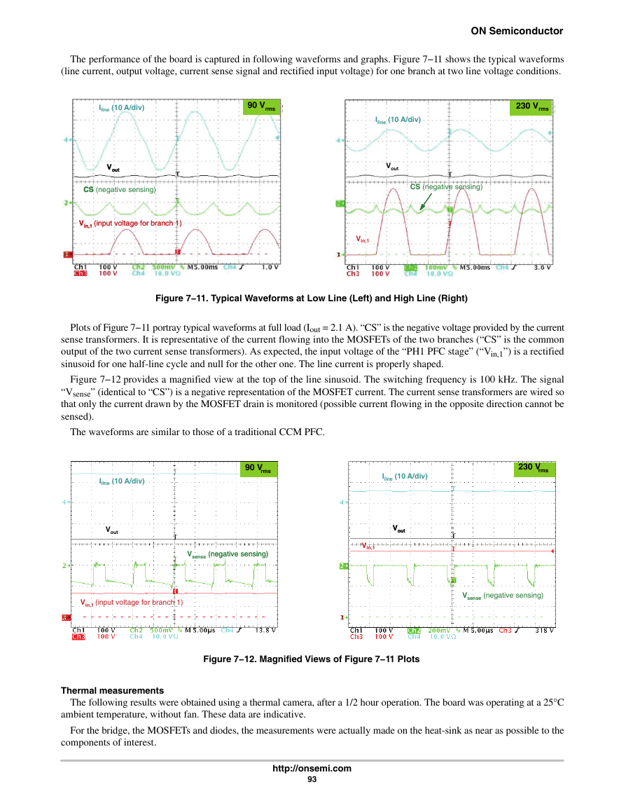
The performance of the board is captured in following waveforms and graphs. Figure 7−11 shows the typical waveforms
(line current, output voltage, current sense signal and rectified input voltage) for one branch at two line voltage conditions.
Iline (10 A/div)
90 Vrms
90 Vrms
230 Vrms
ON Semiconductor
Vout
Vout
CS (negative sensing)
CS
Vin,1 (input voltage for branch 1)
Vin,1 (input voltage for branch 1)
Iline (10 A/div)
Vout
CS (negative sensing)
Vin,1
Figure 7−11. Typical Waveforms at Low Line (Left) and High Line (Right)
Plots of Figure 7−11 portray typical waveforms at full load (Iout = 2.1 A). “CS” is the negative voltage provided by the current
sense transformers. It is representative of the current flowing into the MOSFETs of the two branches (“CS” is the common
output of the two current sense transformers). As expected, the input voltage of the “PH1 PFC stage” (“Vin,1”) is a rectified
sinusoid for one half-line cycle and null for the other one. The line current is properly shaped.
Figure 7−12 provides a magnified view at the top of the line sinusoid. The switching frequency is 100 kHz. The signal
“Vsense” (identical to “CS”) is a negative representation of the MOSFET current. The current sense transformers are wired so
that only the current drawn by the MOSFET drain is monitored (possible current flowing in the opposite direction cannot be
sensed).
The waveforms are similar to those of a traditional CCM PFC.
Iline (10 A/div)
Vout
90 Vrms
90 Vrms
Iline (10 A/div)
230 Vrms
230 Vrms
Vsense (negative sensing)
(negative sensing)
Vout
Vout
Vin,1
Vin,1 (input voltage for branch 1)
Vsense (negative sensing)
Figure 7−12. Magnified Views of Figure 7−11 Plots
Thermal measurements
The following results were obtained using a thermal camera, after a 1/2 hour operation. The board was operating at a 25°C
ambient temperature, without fan. These data are indicative.
For the bridge, the MOSFETs and diodes, the measurements were actually made on the heat-sink as near as possible to the
components of interest.
http://onsemi.com
93
�
PFC Handbook
Measurement Conditions:
Vin(rms) = 88 V
Pin(avg)) = 814 W
Vout = 381 V
Iout = 2 A
PF = 0.995
THD = 9 %
Devices
Bridge MOSFET1 Diode1
Coil1 MOSFET2 Diode2
Coil2
Bulk Capacitor CM EMI coil
Temperature (5C)
85
95
77
47
86
80
48
40
45
Efficiency and Total Harmonic Distortion
100
)
%
(
I
Y
C
N
E
C
F
F
E
I
230 Vrms
120 Vrms
90 Vrms
98
96
94
92
90
100
200
300
400
500
600
700
800
)
%
(
D
H
T
90 Vrms
20
15
10
5
230 Vrms
120 Vrms
0
100
200
300
400
500
600
700
800
900
20% Pmax
OUTPUT POWER (W)
Pmax
20% Pmax
OUTPUT POWER (W)
Pmax
Figure 7−13. Efficiency Performance
Figure 7−14. Total Harmonic Distortion Over the
Load Range
Figure 7−13 portrays the efficiency over the line range, from 20% to 100% of the load.
The efficiency was measured under following conditions:
♦ The measurements were made after the board was operated at full load, low line for 30 minutes
♦ All the measurements were made consecutively without interruptions
♦ PF, THD, Iin(rms) were measured by a power meter PM1200
♦ Vin(rms) was measured directly at the input of the board by a HP 34401A multimeter
♦ Vout was measured by a HP 34401A multimeter
♦ The input power was computed according to: Pin(avg) + Vin(rms) @ Iin(rms) @ PF
♦ Open frame, ambient temperature, no fan
Reviewing Figure 7−13, it can be noted that:
♦ Like in a conventional PFC, the efficiency is higher at high line.
♦ At low line (90 Vrms), full load, the efficiency is in the range of 94% without a fan. When measured @ 100 Vrms
input, full load efficiency of 95% was recorded.
♦ The light load efficiency is very good. For instance, at 20% of full load, efficiency is in the range of or higher than
96%. One of the reasons for this lies in the fact that a bridgeless PFC requires relatively low Qg MOSFETs
compared to a conventional PFC for the same efficiency target at full load.
Figure 7−14 portrays the THD at 90, 120 and 230 Vrms over the load. One can note that the total harmonic distortion remains
very low even in high line, light load (<15%) where the line current is small and more sensitive to all the sources of distortion
like the system inaccuracies and mainly the EMI filter.
http://onsemi.com
94
�
ON Semiconductor
Conclusion
A bridgeless PFC based on the two-phase architecture has several merits among which one can list the ease of control or the
absence of high frequency noise injected to the line (eased EMI). In this chapter, the basics of the bridgeless architecture along
with a summary design procedure are covered. The designed prototype has been tested at full load (800-W output) without a
fan (open frame, ambient temperature). In these conditions, the full-load efficiency was measured in the range of 94% at 90
Vrms and as high as 95% at 100 Vrms. The THD remains very low. A NCP1653 or NCP1654-driven two-phase bridgeless PFC
is a solution of choice for very efficient, high power applications.
It should be noted that when traditional topologies (CCM/CrM/FCCrM boost) are scaled up to high power levels such as
800-W, they encounter several design challenges related to component size and dissipation. Hence, topologies such as
two-phase bridgeless or interleaved, which spread the heat dissipation and offer other benefits, make a lot of sense. Further
information on bridgeless PFC can be found in AND8392 [7] from ON Semiconductor.
Please note that a 300−W bridgeless PFC has been recently experimented. An application note is available on the ON
Semiconductor website that details this application [9].
http://onsemi.com
95
�
PFC Handbook
References
1. Laszlo Huber, Yungtaek Jang and Milan M. Jovanovic, “Performance Evaluation of Bridgeless PFC Boost
Rectifiers”, APEC 2007
2. Pengju Kong, Shuo Wang, and Fred C. Lee, “Common Mode EMI Noise Suppression for Bridgeless PFC
Converters”
3. Alexandre Ferrari de Souza and Ivo Barbi, “High Power Factor Rectifier with Reduced Conduction and
Commutation Losses”, Intelec, 1999
4. Joel Turchi, “Four Key Steps to Design a Continuous Conduction Mode PFC Stage Using the NCP1653”,
AND81842/D, ON Semiconductor, http://www.onsemi.com/pub/Collateral/AND8184D.PDF
5. Patrick Wang, “Four Key Steps to Design a Continuous Conduction Mode PFC Stage Using the NCP1654”,
AND8322/D, ON Semiconductor, http://www.onsemi.com/pub/Collateral/AND8322D.PDF
6. NCP1653 data sheet and application notes, www.onsemi.com
7. NCP1654 data sheet and application notes, www.onsemi.com
8. Joel Turchi, “A 800−W Bridgless PFC Stage”, AND8392/D, ON Semiconductor, http://www.onsemi.com/pub/
Collateral/AND8392−D.PDF
9. Joel Turchi, “A High−Efficiency, 300−W Bridgeless PFC Stage,”AND8481/D, ON Semiconductor,
http://www.onsemi.com/pub/Collateral/AND8481−D.PDF
http://onsemi.com
96
�
CHAPTER 8
Single Stage, Isolated Power Factor Correction
Introduction
Applications that require an isolated, regulated output voltage or current along with input power factor correction typically
involve a two stage conversion process as depicted in Figure 8−1. This scheme is composed of an input boost or bridge−less
power factor corrector stage which converts and pre−regulates the input line into a nominal 400 Vdc bus. This bus then provides
the input voltage for a conventional dc−to−dc converter which can be any appropriate topology. For lower power applications
of 100 W and less, a flyback converter is commonly used.
AC
input
EMI
Filter
Boost
PFC
DC
output
Main
Converter
Figure 8−1. Conventional Two−Stage Conversion
With a few performance compromises, a simpler technique to develop an isolated regulated dc output voltage or current can
be implemented in which the power factor corrector and main converter sections are merged into a single conversion, The
advantage of this approach is reduced parts count and the potential to improve efficiency and power density in lower power
applications. The block diagram is shown in Figure 8−2.
AC
input
EMI
Filter
DC
output
Main
Converter
Figure 8−2. Single Stage Conversion with NCP1652
In this single stage PFC converter, the most useful power circuit is the flyback topology or an equivalent buck−boost
derivation. The flyback stage not only handles the output voltage regulation and input to output isolation functions, but can
provide power factor correction as well. The circuit essentially functions as a conventional boost PFC converter with the output
being derived from an isolated secondary winding on the boost choke rather than using a high voltage diode directly after the
choke as in the conventional high voltage boost mode. The dc input to the converter following the ac bridge rectifier is a
full−wave rectified sine wave, operating at twice the line frequency (100 or 120 Hz) instead of a pure dc voltage. The normal
input “bulk” capacitor following the bridge rectifier must be reduced to a value of 1 μF or less so that the capacitive input filter
does not have any significant effect on the power factor. The value of this capacitor should be sufficient to provide a low
impedance at the converter’s switching frequency, but small enough to offer very high impedance at the ac line frequency.
Single Stage Converter Characteristics
The single stage, isolated PFC converter can be configured from the conventional buck−boost derived flyback topology. The
operational mode can be in discontinuous conduction mode (DCM), critical conduction mode (CrM), or continuous conduction
mode (CCM). The most common operational mode for lower power circuits is CrM because of the overall control simplicity
and ease of implementation of synchronous output rectification for lower voltage outputs (<12 Vdc). The ON Semiconductor
NCL30000 PFC controller is particularly well suited for the lower power applications of 50 W or less which includes LED
lighting applications as well as small power adapters. The CrM operational characteristics will be similar to any conventional
critical conduction mode boost PFC or flyback converter, namely the switching frequency will vary with line and load, and
recovery losses in the output rectifier will be negligible due to the secondary flyback current going to zero prior to re−activation
of the main power switch. This latter characteristic makes it straightforward to implement MOSFET synchronous rectifiers
in designs where low output voltages require minimal conduction losses in the output rectifier. The ON Semiconductor
NCP4302 and NCP4303 are particularly suited for secondary side synchronous rectifier control.
© Semiconductor Components Industries, LLC, 2009
April, 2009 − Rev. 1
97
Publication Order Number:
AND8397/D
�
PFC Handbook
Continuous conduction mode however, can offer significant advantages for applications that require fixed frequency
operation; this is especially true for output voltages of 15 Vdc or higher where the use of synchronous rectification yields
marginal efficiency improvements. In CCM the peak MOSFET current can be significantly less than in CrM resulting in lower
MOSFET switching losses, particularly at power levels above 75 W. CCM operation also reduces the high frequency output
capacitor ripple current, and the overall conversion efficiency is generally higher. The NCP1652 controller is designed
particularly for CCM operation and also provides a second gate drive output for the implementation of an active clamp snubber
for even higher power applications where voltage spikes caused by the flyback transformer’s leakage inductance energy can
become a significant issue.
The single stage PFC conversion process, regardless of the operational mode, has a few compromises over the traditional
two−stage conversion scheme of Figure 8−1. They are as follows:
1. As with any power factor corrector circuit, the gain bandwidth of the control loop is very low, typically in the
10−30 Hz range. This is necessary, otherwise the control loop would attempt to regulate off the line variations of
the input and this would result in poor power factor. As a consequence of the low bandwidth, transient response to
load step changes will be compromised although dc regulation will be excellent. For adapter applications where
point−of−load regulation (POL) is utilized anyway, the slow transient response is inconsequential.
2. Because the loop cannot regulate away the line ripple, it will appear as a ripple component on the output. Therefore
sufficient output capacitance must be utilized to keep the line ripple component minimized for the specific
application. As mentioned previously, the use of downstream POLs in the system should preclude excessive output
capacitance since the ripple will be attenuated sufficiently by the POL regulators. In constant current LED
applications, the low frequency ripple will even be less of an issue as long as the peak current requirement for the
LED is not violated.
3. Due to the lack of a large input bulk capacitor, the converter has no significant inherent hold−up time other than
that provided by the stored energy in the transformer and the output capacitors.
4. The power factor for the single stage converter tends to degrade with increasing line and decreasing load due to
factors related to the duty cycle [D/(1−D)] transfer function and non−linearity effects in the magnetics, however, for
most typical line and load conditions the PF will be above 0.90.
5. Just like any flyback topology, the effects of leakage inductance in the main power transformer will have a direct
impact on performance, EMI, and overall efficiency. The transformer should be wound with proper wire sizing to
minimize AC losses due to skin effect, and winding layers should be kept to a minimum to avoid proximity effect
and winding self−capacitance. In most cases with off−the−shelf cores, the primary will require 2 layers so it is best
to use the “sandwiched” secondary construction where half the primary is wound first, then the secondary, and then
the second half of the primary over the secondary. The primaries are then connected in series externally. This
construction will help minimize the leakage inductance of the magnetic structure. Under no circumstances should
windings be wound in different layers and then paralleled. This construction will result in high circulating currents.
Windings requiring multiple strands of wire should be wound “multifilar” and constrained to two layers or less.
Moreover, the leakage inductance effects will be more prominent the lower the secondary output voltage due to the
coupling effect of the primary to the secondary turns.
Despite these tradeoffs, the single stage, isolated PFC converter is an efficient and very cost effective solution for offline
LED power supply units, notebook adapters and similar applications needing compact size with minimal parts count. For LED
driver applications, an additional current feedback loop with output current sense resistors can be implemented to provide a
constant current, constant voltage (CCCV) characteristic. The ON Semiconductor NCS1002 dual op amp plus reference is well
suited for such applications.
Design Example using the NCL30000
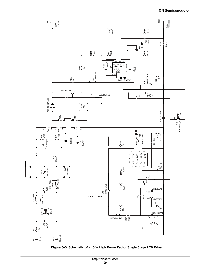
An implementation of a CrM/DCM single stage PFC converter based on the compact SO−8 packaged NCL30000 is shown
in Figure 8−3. This circuit is optimized for driving high brightness LEDs with constant current control but could be modified
for fixed voltage output by changing feedback to a constant voltage configuration. As shown, this circuit provides up to 15
W at a constant 350 mA which is typical for many high brightness LEDs and is capable of powering 4 to 17 white LEDs from
a source spanning 90 to 305 Vac.
http://onsemi.com
98
�
1
-
2
J
1
e
d
o
n
A
D
E
L
6
1
C
F
n
0
0
1
6
6
2
2
R
R
k
6
1
7
7
2
2
R
R
0
0
0
0
2
2
3
25 6 4
5
5
2
2
R
R
k
1
F
p
0
0
1
4
1
C
6
5
C
4
8
X
Z
B
2
1
D
3
2
R
k
1
MMBTA06
Q4
+
1
N
I
−
1
N
I
+
2
N
I
−
2
N
I
D
N
G
3
3
U
U
C
C
V
1
T
U
O
2
T
U
O
8 1 7
4
0
9
2
M
L
5
1
C
F
n
0
2
2
D13 BAW56
ON Semiconductor
2
-
2
J
1
e
d
o
h
t
a
C
D
E
L
W
2
0
.
1
1
3
3
R
R
k
4
2
0
3
R
k
4
2
8
8
2
2
R
R
0
0
7
7
4
4
A
A
1
1
3
3
4
4
L
L
T
T
4
4
U
U
9
2
R
6
6
0
0
A
A
T
T
B
B
M
M
M
M
5
5
Q
Q
4
2
R
k
7
4
D11
BZX84C5V6
2
2
2
2
R
R
k
1
C13
100nF
F
n
7
.
4
0
1
C
1
4
2
3
2
U
1
_
L
1
6
5
2
S
P
6
1
R
k
7
4
F
u
0
1
8
C
5
1
R
k
0
0
1
1
1
R
k
0
0
1
6
0
A
T
B
M
M
2
Q
BAW56 D7
0
1
R
k
2
6
.
3
Q
0
8
N
2
0
D
P
S
0
0
1
1
9
9
1
1
R
R
0
2
R
0
0
0
0
1
1
8
8
1
1
R
R
W
3
3
0
.
678
5
0
0
0
0
3
L
C
N
C
C
V
P
F
M
V
R
D
p
m
o
C
D
N
G
D
C
Z
t
C
S
C
1 2 3
4
F
p
0
2
8
9
C
7
1
R
0
0
1
7
7
C
C
F
n
1
4
1
R
k
7
4
.
MMBZ5245
D9
15V
Q1
MMBTA06
T
1
T
R
BZX84C5V1
D8
5.1V
R9 6.2k
0
3
3
D
R
U
M
0
1
D
+
+
2
1
C
F
u
0
7
4
D
1
T
E
1
T
4
3
A
1
T
3 5
B
1
T
1
2
C
1
T
K
7
4
7
R
K
7
4
6
R
F
p
0
0
7
4
5
C
5
D
M
1
S
E
6
D
1
2
S
A
B
4
4
C
C
F
n
0
0
1
1
V
R
4
A
L
0
0
3
V
4
D
7
0
0
4
A
R
M
6
K
5
3
R
F
F
n
n
7
7
4
4
2
2
C
C
H
m
2
.
2
3
L
H
m
2
2
.
2
L
6
K
5
2
R
3
1
L
1
4
2
H
m
7
2
1
C
F
n
7
4
1
F
1
-
1
J
A
1
1
e
n
L
i
1
2
-
1
J
l
a
r
t
u
e
N
Figure 8−3. Schematic of a 15 W High Power Factor Single Stage LED Driver
http://onsemi.com
99
�








 2023年江西萍乡中考道德与法治真题及答案.doc
 2012年重庆南川中考生物真题及答案.doc
 2013年江西师范大学地理学综合及文艺理论基础考研真题.doc
 2020年四川甘孜小升初语文真题及答案I卷.doc
 2020年注册岩土工程师专业基础考试真题及答案.doc
 2023-2024学年福建省厦门市九年级上学期数学月考试题及答案.doc
 2021-2022学年辽宁省沈阳市大东区九年级上学期语文期末试题及答案.doc
 2022-2023学年北京东城区初三第一学期物理期末试卷及答案.doc
 2018上半年江西教师资格初中地理学科知识与教学能力真题及答案.doc
 2012年河北国家公务员申论考试真题及答案-省级.doc
 2020-2021学年江苏省扬州市江都区邵樊片九年级上学期数学第一次质量检测试题及答案.doc
 2022下半年黑龙江教师资格证中学综合素质真题及答案.doc