A V A I L A B L E
Maxim > App Notes > Amplifier and Comparator Circuits Power-Supply Circuits
Keywords: powered device, PD, power over Ethernet, PoE, IEEE 802.3af, IEEE 802.3at, Class 2 PD, Class 3 PD, IP phones, IP cameras, security cameras, WAP, wireless access point, point
of sales, POS, thin client, Ethernet repeater, active clamped forward, flyback
Feb 10, 2011
APPLICATION NOTE 4984
High-Efficiency, Low Cost Flyback Converter Uses No Optocoupler Feedback
Abstract: This reference design is for a highly efficient, flyback, 12V, Class 3 powered device (PD). The design features the MAX5969B as its controller. The design also
uses the MAX5974A, which controls current-mode PWM converters and provides frequency foldback for PoE applications. Using these devices, this reference design is
IEEE® 802.3af/at compliant and is a high-performance, compact, and cost efficient solution for a Class 3 PD. The design can also be customized to 12V/2A Class 4 PD.
General Description
This reference design is for a highly efficient, flyback, 12V/1A Class 3 powered device (PD) that is IEEE 802.3af/3at complaint and cost effective. The reference design can
be customized to a 12V/2A Class 4 PD.
The design features the MAX5969B and MAX5974A. The MAX5969B controller is fully compliant with the IEEE 802.3af/at standard in a power-over-Ethernet (PoE) system.
The device can also get power from a wall adapter (WAD). The MAX5974A controls wide-input-voltage, active-clamped, inductive feedback, current-mode PWM converters
and provides frequency foldback for PoE applications. Using these devices, this reference design is IEEE 802.3af/at compliant. It is also a high-performance, compact, and
economical solution for a Class 3 PD or a Class 4 PD.
Specifications
The 12V/1A PD meets the following specifications:
Input voltage: 36V to 57V
WAD input voltage: 36V to 57V (10V to 57V with a different transformer)
VOUT1: 12V/1A (up to 2A by optimizing the switching frequency)
Output ripple: ±2.5% (can be reduced by adding more output ceramic capacitors or disabling the frequency foldback, FFB)
Load transient VP-P: ±3% (25% step-load)
Line and load regulation: ±2%
Switching frequency: 300kHz (150kHz in FFB mode)
Total efficiency with a load of 2A at 3V and 48V input: 90.3%, including input LAN transformer and diode bridge (93.3%, not including input LAN transformer and
diode bridge)
Design Features
Inductive feedback: no optocoupler or shunt-regulator, so costs are lowered
Self-driving input voltage: achieves synchronous rectifier, provides high efficiency and good load regulation
Frequency foldback: 150kHz switching frequency when load is about 1W, provides high efficiency at light loads
Page 1 of 4�
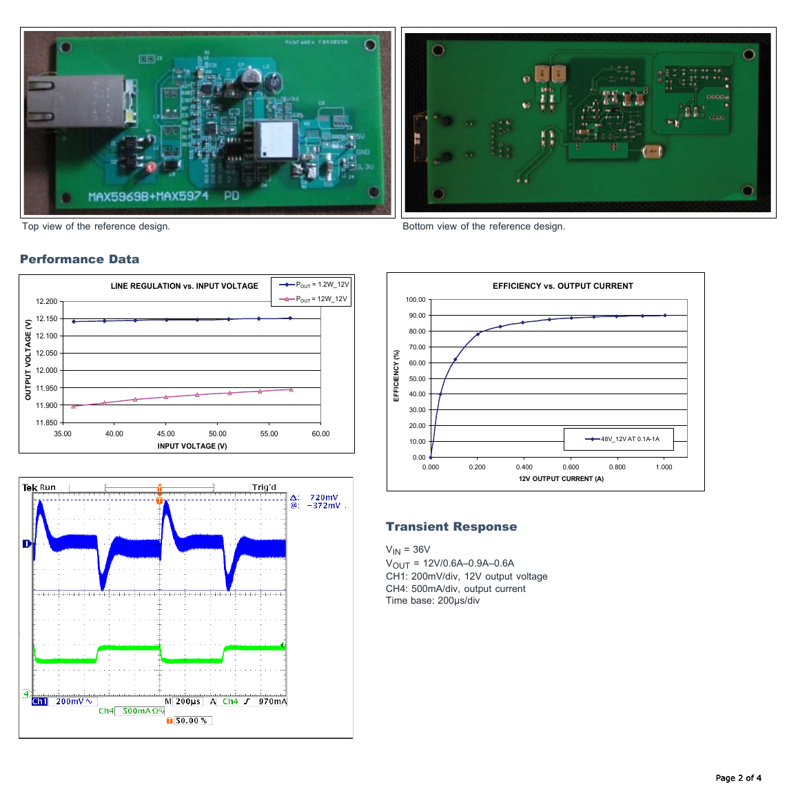
Top view of the reference design.
Bottom view of the reference design.
Performance Data
LINE REGULATION vs. INPUT VOLTAGE
POUT = 1.2W_12V
POUT = 12W_12V
)
V
(
E
G
A
T
L
O
V
T
U
P
T
U
O
12.200
12.150
12.100
12.050
12.000
11.950
11.900
11.850
35.00
40.00
50.00
45.00
INPUT VOLTAGE (V)
55.00
60.00
)
%
(
I
Y
C
N
E
C
F
F
E
I
EFFICIENCY vs. OUTPUT CURRENT
48V_12V AT 0.1A-1A
100.00
90.00
80.00
70.00
60.00
50.00
40.00
30.00
20.00
10.00
0.00
0.000
0.200
0.400
12V OUTPUT CURRENT (A)
0.600
0.800
1.000
Transient Response
VIN = 36V
VOUT = 12V/0.6A–0.9A–0.6A
CH1: 200mV/div, 12V output voltage
CH4: 500mA/div, output current
Time base: 200µs/div
Page 2 of 4
Page 2 of 4
Page 2 of 4�
2
1
2
D
C
1
TX1+P1
TX1-P2
TX2+P3
TX2-P6
TX3+P4
TX3-P5
TX4+P7
TX4-P8
1
2
2
2
TD1+
TC1
TD1-
VC1
TD2+
TC2
TD2-
VC2
TD3+
TC3
TD3-
VC3
TD4+
CT
TD4-
VC4
1
G
2
G
1
Y
2
Y
7
1
8
1
9
1
0
2
J1
11
12
10
13
4
6
5
14
3
1
2
15
8
7
9
16
T
U
O
A
T
A
D
VDD
VDD
2
C
A
2
C
A
D1
C
A
1
D2
C
A
1
3
+
V
-
V
4
3
+
V
-
V
4
R7
C3
R6
VSS
C14
VSS
N
I
R
E
W
O
P
&
A
T
A
D
R15
R16
RTN
B
VDD
VDD
R1
D3
C2
VSS
VSS
A
U1
MAX5969B
VDD
DET
N.C.
N.C.
CLS
2EC
PG
WAD
VSS
P
E
RTN
1
2
3
4
5
10
CLS
PG
9
8
7
6
P
E
R4
RTN
CLS
1
2
3
Title
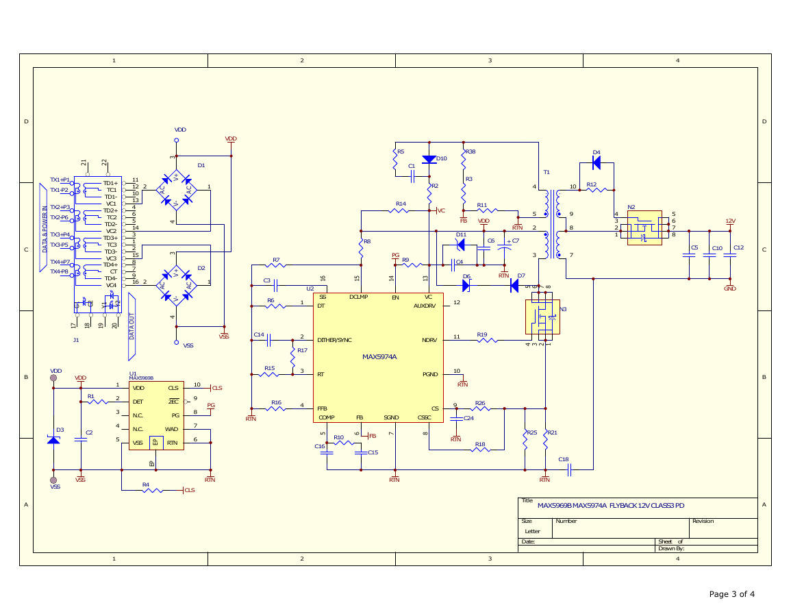
MAX5969B MAX5974A FLYBACK 12V CLASS3 PD
Size
Letter
:etaD
Number
Revision
fo teehS
Drawn By:
4
B
A
3
4
D
D4
T1
10
R12
9
8
7
N2
4
3
2
1
5
6
7
8
12V
C5
C10
C12
C
GND
R5
C1
R14
D10
R2
VC
R38
R3
R11
FB
VDD
4
5
2
3
RTN
C6
+ C7
RTN
D7
567
8
N3
R19
1234
R8
PG
R9
U2
6
1
SS
DT
5
1
4
1
3
1
DCLMP
EN
VC
AUXDRV
DITHER/SYNC
NDRV
MAX5974A
PGND
D11
C4
D6
12
11
10
RTN
R17
3
4
RT
FFB
COMP
FB
SGND
CSSC
C24
CS
9
R26
5
R10
6
FB
7
8
C16
C15
RTN
R18
RTN
R25
R21
C18
RTN
Page 3 of 4�
IEEE is a registered service mark of the Institute of Electrical and Electronics Engineers, Inc.
Related Parts
MAX5969B IEEE 802.3af/at-Compliant, Powered Device Interface Controllers with Integrated Power MOSFET
MAX5974A Active-Clamped, Spread-Spectrum, Current-Mode PWM Controllers
Automatic Updates
Would you like to be automatically notified when new application notes are published in your areas of interest? Sign up for EE-Mail™.
Application note 4984: www.maxim-ic.com/an4984
More information
For technical support: www.maxim-ic.com/support
For samples: www.maxim-ic.com/samples
Other questions and comments: www.maxim-ic.com/contact
AN4984, AN 4984, APP4984, Appnote4984, Appnote 4984
Copyright © by Maxim Integrated Products
Additional legal notices: www.maxim-ic.com/legal
Page 4 of 4�


 2023年江西萍乡中考道德与法治真题及答案.doc
 2012年重庆南川中考生物真题及答案.doc
 2013年江西师范大学地理学综合及文艺理论基础考研真题.doc
 2020年四川甘孜小升初语文真题及答案I卷.doc
 2020年注册岩土工程师专业基础考试真题及答案.doc
 2023-2024学年福建省厦门市九年级上学期数学月考试题及答案.doc
 2021-2022学年辽宁省沈阳市大东区九年级上学期语文期末试题及答案.doc
 2022-2023学年北京东城区初三第一学期物理期末试卷及答案.doc
 2018上半年江西教师资格初中地理学科知识与教学能力真题及答案.doc
 2012年河北国家公务员申论考试真题及答案-省级.doc
 2020-2021学年江苏省扬州市江都区邵樊片九年级上学期数学第一次质量检测试题及答案.doc
 2022下半年黑龙江教师资格证中学综合素质真题及答案.doc