Computer Organization and Architecture
Course Design
The Report of the parallel output controller
(POC)
School of Information Science and Engineering
Southeast University
March 2013
1
�
Contents
1. Purpose--------------------------------------------------
2. Tasks-----------------------------------------------------
3. The overall connection-------------------------------
4. Design description-------------------------------------
5. Simulation result-------------------------------------
6. Conclusion and discussion---------------------------
7. Appendix---------------------------------------------
2
�
1. Purpose
The purpose of this project is to design and simulate a parallel output controller
(POC)which acts an interface between system bus and printer. The Altera’s Maxplus
II EDA tool is recommended and provided for simulation. Please refer to William
Stallings.“Computer Organization and Architecture, Designing for Performance”,
P.65~75; P.185~190.
2. Tasks
Basic introduction: POC is one of the most common I/O modules, namely the
parallel output controller. It plays therole of an interface between the computer system
bus and the peripheral (such as a printer or otheroutput devices).
Architectural Model:
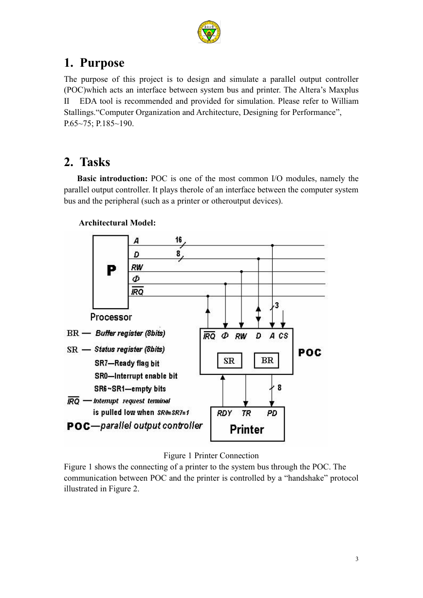
Figure 1 Printer Connection
Figure 1 shows the connecting of a printer to the system bus through the POC. The
communication between POC and the printer is controlled by a “handshake” protocol
illustrated in Figure 2.
3
�
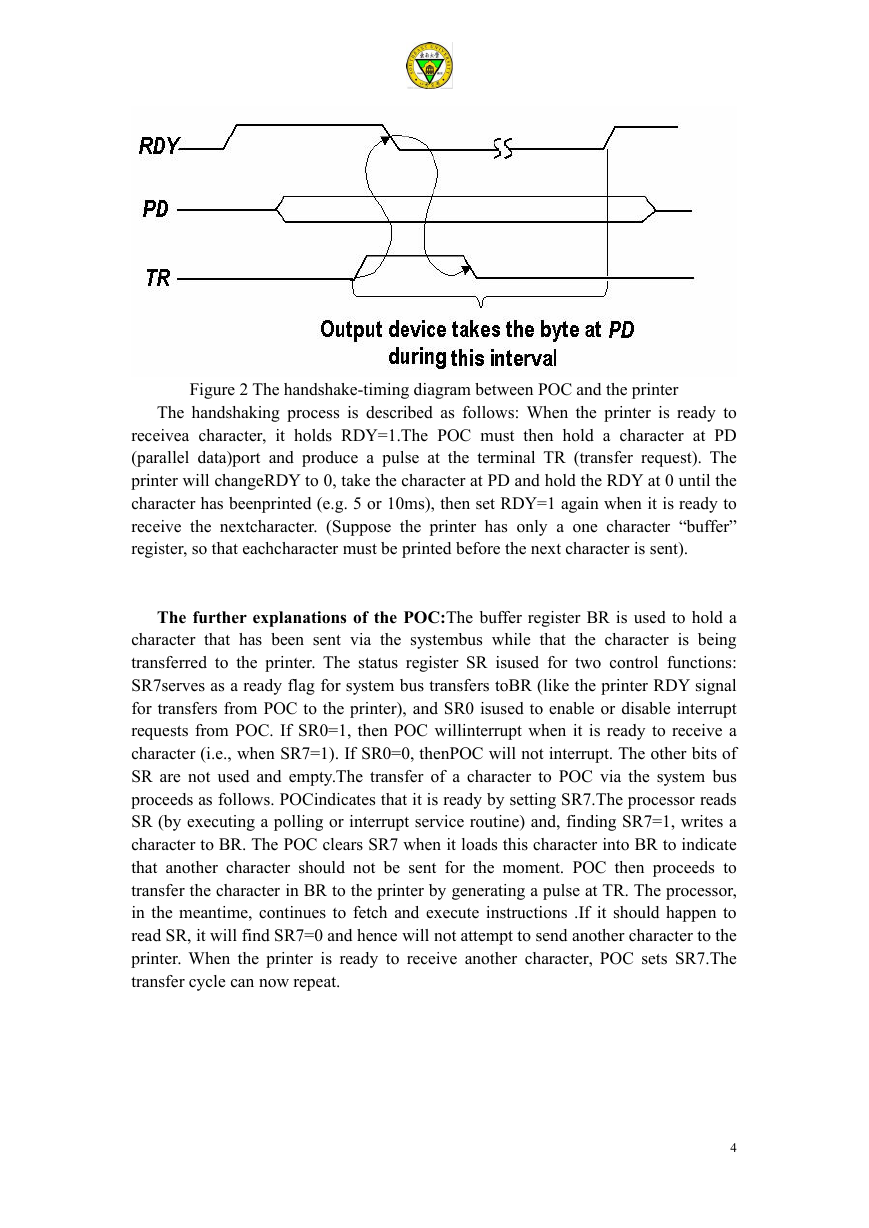
Figure 2 The handshake-timing diagram between POC and the printer
The handshaking process is described as follows: When the printer is ready to
receivea character, it holds RDY=1.The POC must then hold a character at PD
(parallel data)port and produce a pulse at the terminal TR (transfer request). The
printer will changeRDY to 0, take the character at PD and hold the RDY at 0 until the
character has beenprinted (e.g. 5 or 10ms), then set RDY=1 again when it is ready to
receive the nextcharacter. (Suppose the printer has only a one character “buffer”
register, so that eachcharacter must be printed before the next character is sent).
The further explanations of the POC:The buffer register BR is used to hold a
character that has been sent via the systembus while that the character is being
transferred to the printer. The status register SR isused for two control functions:
SR7serves as a ready flag for system bus transfers toBR (like the printer RDY signal
for transfers from POC to the printer), and SR0 isused to enable or disable interrupt
requests from POC. If SR0=1, then POC willinterrupt when it is ready to receive a
character (i.e., when SR7=1). If SR0=0, thenPOC will not interrupt. The other bits of
SR are not used and empty.The transfer of a character to POC via the system bus
proceeds as follows. POCindicates that it is ready by setting SR7.The processor reads
SR (by executing a polling or interrupt service routine) and, finding SR7=1, writes a
character to BR. The POC clears SR7 when it loads this character into BR to indicate
that another character should not be sent for the moment. POC then proceeds to
transfer the character in BR to the printer by generating a pulse at TR. The processor,
in the meantime, continues to fetch and execute instructions .If it should happen to
read SR, it will find SR7=0 and hence will not attempt to send another character to the
printer. When the printer is ready to receive another character, POC sets SR7.The
transfer cycle can now repeat.
4
�
3. The overall connection of the simulated printer
and POC expressed in the top module form
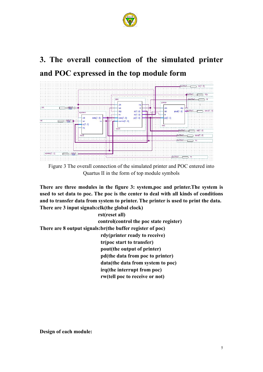
Figure 3 The overall connection of the simulated printer and POC entered into
Quartus II in the form of top module symbols
There are three modules in the figure 3: system,poc and printer.The system is
used to set data to poc. The poc is the center to deal with all kinds of conditions
and to transfer data from system to printer. The printer is used to print the data.
There are 3 input signals:clk(the global clock)
rst(reset all)
control(control the poc state register)
There are 8 output signals:br(the buffer register of poc)
rdy(printer ready to receive)
tr(poc start to transfer)
pout(the output of printer)
pd(the data from poc to printer)
data(the data from system to poc)
irq(the interrupt from poc)
rw(tell poc to receive or not)
Design of each module:
5
�
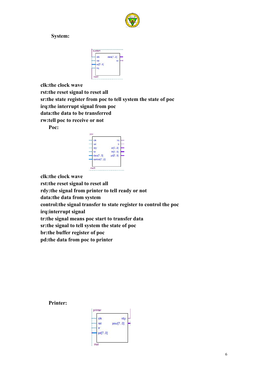
System:
clk:the clock wave
rst:the reset signal to reset all
sr:the state register from poc to tell system the state of poc
irq:the interrupt signal from poc
data:the data to be transferred
rw:tell poc to receive or not
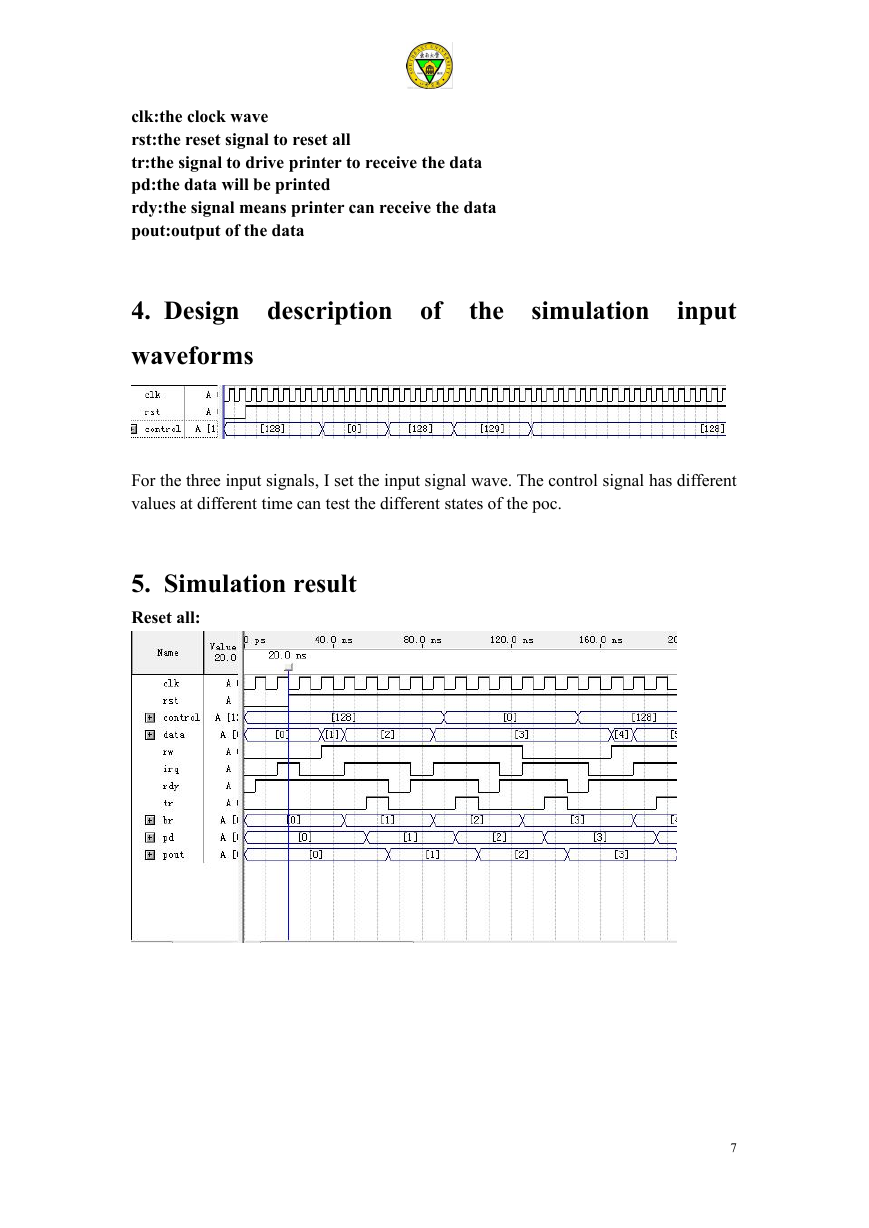
Poc:
clk:the clock wave
rst:the reset signal to reset all
rdy:the signal from printer to tell ready or not
data:the data from system
control:the signal transfer to state register to control the poc
irq:interrupt signal
tr:the signal means poc start to transfer data
sr:the signal to tell system the state of poc
br:the buffer register of poc
pd:the data from poc to printer
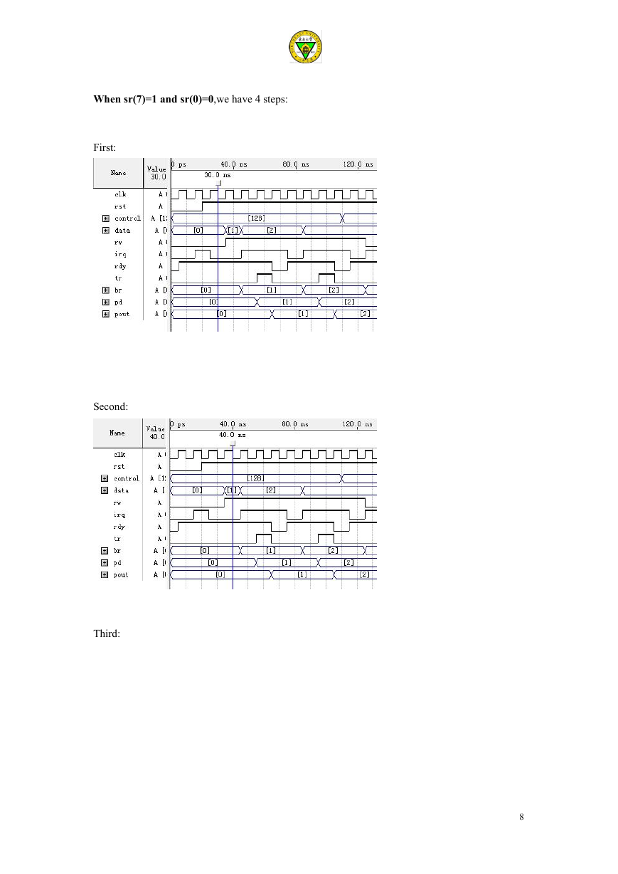
Printer:
6
�
clk:the clock wave
rst:the reset signal to reset all
tr:the signal to drive printer to receive the data
pd:the data will be printed
rdy:the signal means printer can receive the data
pout:output of the data
4. Design description of
waveforms
the
simulation input
For the three input signals, I set the input signal wave. The control signal has different
values at different time can test the different states of the poc.
5. Simulation result
Reset all:
7
�
When sr(7)=1 and sr(0)=0,we have 4 steps:
First:
Second:
Third:
8
�


 2023年江西萍乡中考道德与法治真题及答案.doc
 2012年重庆南川中考生物真题及答案.doc
 2013年江西师范大学地理学综合及文艺理论基础考研真题.doc
 2020年四川甘孜小升初语文真题及答案I卷.doc
 2020年注册岩土工程师专业基础考试真题及答案.doc
 2023-2024学年福建省厦门市九年级上学期数学月考试题及答案.doc
 2021-2022学年辽宁省沈阳市大东区九年级上学期语文期末试题及答案.doc
 2022-2023学年北京东城区初三第一学期物理期末试卷及答案.doc
 2018上半年江西教师资格初中地理学科知识与教学能力真题及答案.doc
 2012年河北国家公务员申论考试真题及答案-省级.doc
 2020-2021学年江苏省扬州市江都区邵樊片九年级上学期数学第一次质量检测试题及答案.doc
 2022下半年黑龙江教师资格证中学综合素质真题及答案.doc