TEA19161T
Digital controller for high-efficiency resonant power supply
Rev. 1 — 10 March 2016
Product data sheet
1. General description
The TEA19161T is a fully digital controller for high-efficiency resonant power supplies.
Together with the TEA19162T PFC controller and the TEA1995T dual SR controller, a
complete resonant power supply can be built which is easy to design and has a very low
component count. This power supply meets the efficiency regulations of Energy Star, the
Department of Energy (DoE), the Eco-design directive of the European Union, the
European Code of Conduct, and other guidelines. So, any auxiliary low-power supply can
be omitted.
In contrast to traditional resonant topologies, the TEA19161T (LLC) shows a high
efficiency at low loads due to the newly introduced low-power mode. This mode operates
in the power region between continuous switching (also called high-power mode) and
burst mode.
Because the TEA19161T is regulated via the primary capacitor voltage, it has accurate
information about the power delivered to the output. The measured output power defines
the mode of operation (burst mode, low-power mode or high-power mode). A
configuration pin can easily set the transition levels of the operating modes.
The TEA19161T contains a low-voltage die with a fully digital controller for output power
control, start-up, initializations, and protections. These protections include OverCurrent
Protection (OCP), OverVoltage Protection (OVP), Open-Loop Protection (OLP), and
Capacitive Mode Regulation (CMR). It also contains a high-voltage Silicon-On-Insulator
(SOI) controller for high-voltage start-up, integrated drivers, level shifter, protections, and
circuitry assuring zero-voltage switching.
The TEA19161T is designed to cooperate with the TEA19162T Power Factor Control
(PFC) controller. For communications about start-up and protections, the TEA19161T
contains a digital control interface. The digital control enables a fast latch reset
mechanism. It maximizes the overall system efficiency at low output power levels by
setting the TEA19162T to operate in burst mode.
The TEA19161T/TEA19162T/TEA1995T combination gives an easy to design, highly
efficient and reliable power supply, providing 90 W to 500 W, with a minimum of external
components. The system provides a very low no-load input power (< 75 mW; total system
including the TEA19161T/TEA19162T/TEA1995T combination) and high efficiency from
minimum to maximum load. So, any additional low-power supply can be omitted, ensuring
a significant system cost saving and highly simplified power supply design.
�
NXP Semiconductors
Digital controller for high-efficiency resonant power supply
TEA19161T
2. Features and benefits
2.1 Distinctive features
Complete functionality as a combination with TEA19162T
Integrated high-voltage start-up
Integrated high-voltage Level Shifter (LS)
Extremely fast start-up (< 500 ms at Vmains = 100 V (AC))
Continuously VSUPIC regulation via the SUPHV pin during start-up and protection,
allowing minimum SUPIC capacitor values
Operating frequencies are outside the audible area at all operating modes
Integrated soft start
Power good function
Maximum 500 kHz half-bridge switching frequency
2.2 Green features
Extremely high efficiency from low load to high load
Compliant with Energy using Product directive (EuP) lot 6
Excellent no-load input power (< 75 mW for TEA19161T/TEA19162T/TEA1995T
combination)
Regulated low optocurrent, enabling low no-load power consumption
Very low supply current during non-switching state in burst mode
Transition between different operation modes (high-power/low-power/burst mode)
occur at integrated, externally adjustable power levels
Adaptive non-overlap time
2.3 Protection features
Supply UnderVoltage Protection (UVP)
OverPower Protection (OPP)
Integrated adjustable overpower time-out
Adjustable latch or restart function for OverPower Protection
On-chip OverTemperature Protection (OTP)
Capacitive Mode Regulation (CMR)
Accurate OverVoltage Protection (OVP)
Maximum on-time protection for low-side and high-side driver output
OverCurrent Protection (OCP)
Disable input
3. Applications
Desktop and all-in-one PCs
LCD television
Notebook adapter
Printers
TEA19161T
Product data sheet
All information provided in this document is subject to legal disclaimers.
Rev. 1 — 10 March 2016
© NXP Semiconductors N.V. 2016. All rights reserved.
2 of 46
�
NXP Semiconductors
4. Ordering information
Digital controller for high-efficiency resonant power supply
TEA19161T
Table 1.
Type number
TEA19161T
Ordering information
Package
Name
SO16
Description
plastic small outline package; 16 leads; body width 3.9 mm; body thickness
1.47 mm
Version
SOT109-3
TEA19161T
Product data sheet
All information provided in this document is subject to legal disclaimers.
Rev. 1 — 10 March 2016
© NXP Semiconductors N.V. 2016. All rights reserved.
3 of 46
�
xxxxxxxxxxxxxxxxxxxxx xxxxxxxxxxxxxxxxxxxxxxxxxx xxxxxxx x x x xxxxxxxxxxxxxxxxxxxxxxxxxxxxxx xxxxxxxxxxxxxxxxxxx xx xx xxxxx
xxxxxxxxxxxxxxxxxxxxxxxxxxx xxxxxxxxxxxxxxxxxxx xxxxxx xxxxxxxxxxxxxxxxxxxxxxxxxxxxxxxxxxx xxxxxxxxxxxx x x
xxxxxxxxxxxxxxxxxxxxx xxxxxxxxxxxxxxxxxxxxxxxxxxxxxx xxxxx xxxxxxxxxxxxxxxxxxxxxxxxxxxxxxxxxxxxxxxxxxxxxxxxxx xxxxxxxx
xxxxxxxxxxxxxxxxxxxxxxxxx xxxxxxxxxxxxxxxxxxxx xxx
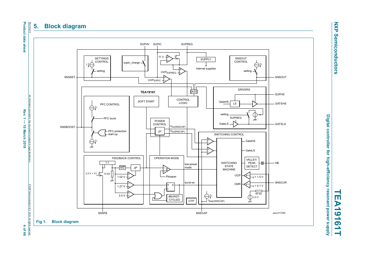
5. Block diagram
Fig 1. Block diagram
T
E
A
1
9
1
6
1
T
P
r
o
d
u
c
t
d
a
t
a
s
h
e
e
t
A
l
l
i
f
n
o
r
m
a
t
i
o
n
p
r
o
v
d
e
d
i
i
n
t
i
h
s
d
o
c
u
m
e
n
t
i
s
s
u
b
e
c
t
t
j
o
l
i
e
g
a
l
d
s
c
a
m
e
r
s
.
l
i
©
N
X
P
S
e
m
c
o
n
d
u
c
t
i
o
r
s
N
V
.
.
2
0
1
6
.
A
l
l
r
i
g
h
t
s
r
e
s
e
r
v
e
d
.
R
e
v
.
1
—
1
0
M
a
r
c
h
2
0
1
6
4
o
f
4
6
i
N
X
P
S
e
m
c
o
n
d
u
c
t
o
r
s
i
D
g
i
t
a
l
c
o
n
t
r
o
l
l
e
r
f
o
r
h
g
h
-
e
f
f
i
i
c
i
e
n
c
y
r
e
s
o
n
a
n
t
p
o
w
e
r
s
u
p
p
l
y
T
E
A
1
9
1
6
1
T
�
NXP Semiconductors
Digital controller for high-efficiency resonant power supply
TEA19161T
6. Pinning information
6.1 Pinning
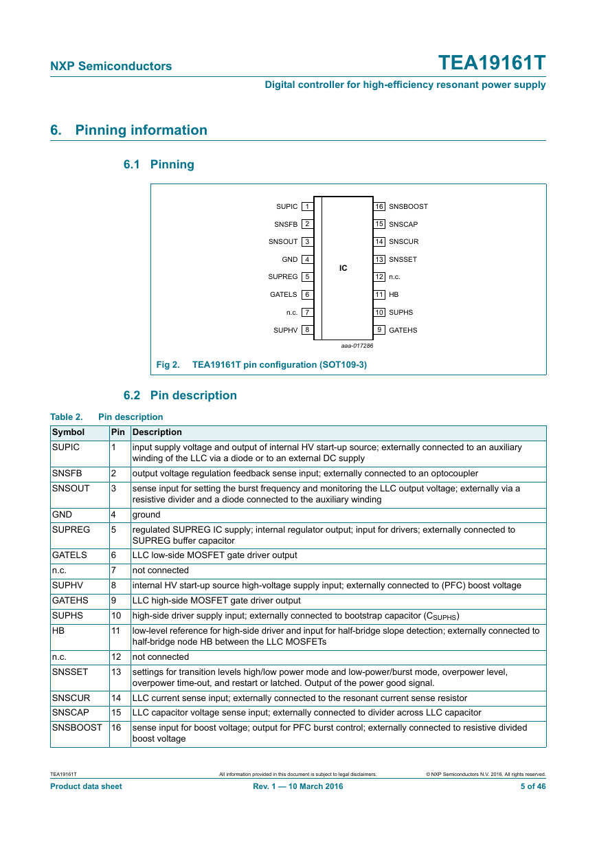
Fig 2.
TEA19161T pin configuration (SOT109-3)
6.2 Pin description
Pin description
Pin Description
1
2
3
4
5
6
7
8
9
10
11
12
13
input supply voltage and output of internal HV start-up source; externally connected to an auxiliary
winding of the LLC via a diode or to an external DC supply
output voltage regulation feedback sense input; externally connected to an optocoupler
sense input for setting the burst frequency and monitoring the LLC output voltage; externally via a
resistive divider and a diode connected to the auxiliary winding
ground
regulated SUPREG IC supply; internal regulator output; input for drivers; externally connected to
SUPREG buffer capacitor
LLC low-side MOSFET gate driver output
not connected
internal HV start-up source high-voltage supply input; externally connected to (PFC) boost voltage
LLC high-side MOSFET gate driver output
high-side driver supply input; externally connected to bootstrap capacitor (CSUPHS)
low-level reference for high-side driver and input for half-bridge slope detection; externally connected to
half-bridge node HB between the LLC MOSFETs
not connected
settings for transition levels high/low power mode and low-power/burst mode, overpower level,
overpower time-out, and restart or latched. Output of the power good signal.
LLC current sense input; externally connected to the resonant current sense resistor
LLC capacitor voltage sense input; externally connected to divider across LLC capacitor
sense input for boost voltage; output for PFC burst control; externally connected to resistive divided
boost voltage
Table 2.
Symbol
SUPIC
SNSFB
SNSOUT
GND
SUPREG
GATELS
n.c.
SUPHV
GATEHS
SUPHS
HB
n.c.
SNSSET
14
SNSCUR
SNSCAP
15
SNSBOOST 16
TEA19161T
Product data sheet
All information provided in this document is subject to legal disclaimers.
Rev. 1 — 10 March 2016
© NXP Semiconductors N.V. 2016. All rights reserved.
5 of 46
�
NXP Semiconductors
Digital controller for high-efficiency resonant power supply
TEA19161T
7. Functional description
7.1 Supply voltages
The TEA19161T includes:
• A high-voltage supply pin for start-up (SUPHV)
• A general supply to be connected to an external auxiliary winding (SUPIC pin)
• An accurate regulated voltage (SUPREG pin)
• A floating supply for the high-side driver (SUPHS pin)
7.1.1 Start-up and supply voltage
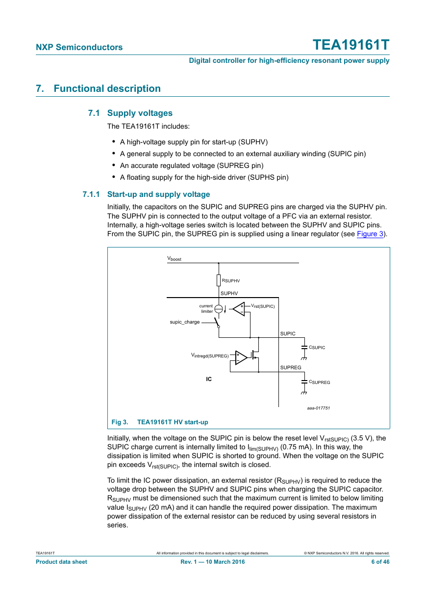
Initially, the capacitors on the SUPIC and SUPREG pins are charged via the SUPHV pin.
The SUPHV pin is connected to the output voltage of a PFC via an external resistor.
Internally, a high-voltage series switch is located between the SUPHV and SUPIC pins.
From the SUPIC pin, the SUPREG pin is supplied using a linear regulator (see Figure 3).
Fig 3.
TEA19161T HV start-up
Initially, when the voltage on the SUPIC pin is below the reset level VrstSUPIC) (3.5 V), the
SUPIC charge current is internally limited to Ilim(SUPHV) (0.75 mA). In this way, the
dissipation is limited when SUPIC is shorted to ground. When the voltage on the SUPIC
pin exceeds Vrst(SUPIC), the internal switch is closed.
To limit the IC power dissipation, an external resistor (RSUPHV) is required to reduce the
voltage drop between the SUPHV and SUPIC pins when charging the SUPIC capacitor.
RSUPHV must be dimensioned such that the maximum current is limited to below limiting
value ISUPHV (20 mA) and it can handle the required power dissipation. The maximum
power dissipation of the external resistor can be reduced by using several resistors in
series.
TEA19161T
Product data sheet
All information provided in this document is subject to legal disclaimers.
Rev. 1 — 10 March 2016
© NXP Semiconductors N.V. 2016. All rights reserved.
6 of 46
�
NXP Semiconductors
Digital controller for high-efficiency resonant power supply
TEA19161T
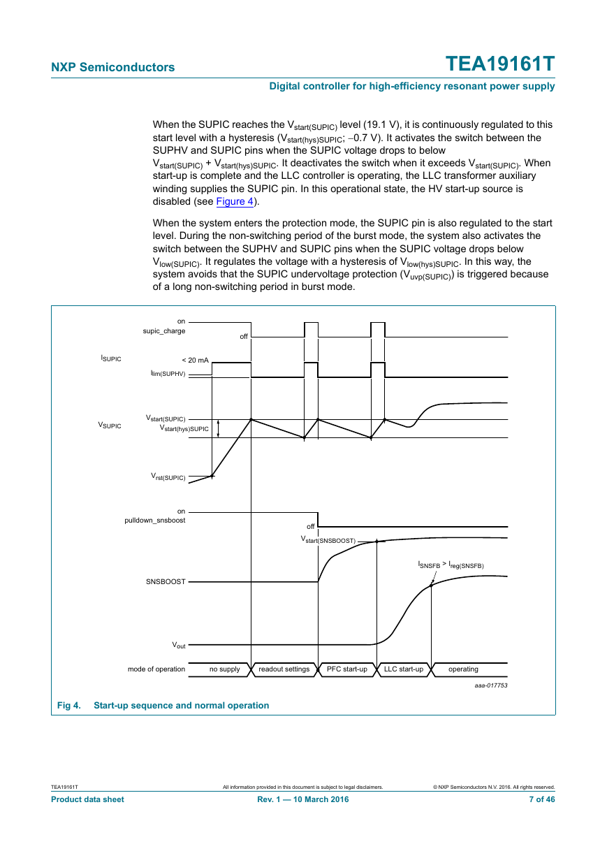
When the SUPIC reaches the Vstart(SUPIC) level (19.1 V), it is continuously regulated to this
start level with a hysteresis (Vstart(hys)SUPIC; 0.7 V). It activates the switch between the
SUPHV and SUPIC pins when the SUPIC voltage drops to below
Vstart(SUPIC) + Vstart(hys)SUPIC. It deactivates the switch when it exceeds Vstart(SUPIC). When
start-up is complete and the LLC controller is operating, the LLC transformer auxiliary
winding supplies the SUPIC pin. In this operational state, the HV start-up source is
disabled (see Figure 4).
When the system enters the protection mode, the SUPIC pin is also regulated to the start
level. During the non-switching period of the burst mode, the system also activates the
switch between the SUPHV and SUPIC pins when the SUPIC voltage drops below
Vlow(SUPIC). It regulates the voltage with a hysteresis of Vlow(hys)SUPIC. In this way, the
system avoids that the SUPIC undervoltage protection (Vuvp(SUPIC)) is triggered because
of a long non-switching period in burst mode.
Fig 4.
Start-up sequence and normal operation
TEA19161T
Product data sheet
All information provided in this document is subject to legal disclaimers.
Rev. 1 — 10 March 2016
© NXP Semiconductors N.V. 2016. All rights reserved.
7 of 46
�
NXP Semiconductors
Digital controller for high-efficiency resonant power supply
TEA19161T
7.1.2 Regulated supply (SUPREG pin)
The voltage range on the SUPIC pin exceeds that of the maximum external MOSFETs
gate-source voltage. So, the TEA19161T incorporates an integrated series stabilizer. The
series stabilizer creates an accurate regulated voltage (Vintregd(SUPREG) = 11 V) at the
buffer capacitor CSUPREG. The stabilized voltage is used to:
• Supply the internal low-side LLC driver
• Supply the internal high-side driver using external components
• As a reference voltage for optional external circuits
To ensure that the external MOSFETs receive sufficient gate drive, the voltage on the
SUPREG pin must reach Vuvp(SUPREG) before the system starts switching. If the SUPREG
voltage drops to below this undervoltage protection level, the system restarts.
7.1.3 High-side driver floating supply (SUPHS pin)
External bootstrap buffer capacitor CSUPHS supplies the high-side driver. The bootstrap
capacitor is connected between the high-side driver supply, the SUPHS pin, and the
half-bridge node, HB. CSUPHS is charged from the SUPREG pin using an external diode
DSUPHS (see Figure 27).
Careful selection of the appropriate diode minimizes the voltage drop between the
SUPREG and SUPHS pins, especially when large MOSFETs and high switching
frequencies are used. A large voltage drop across the diode reduces the gate drive of the
high-side MOSFET.
TEA19161T
Product data sheet
All information provided in this document is subject to legal disclaimers.
Rev. 1 — 10 March 2016
© NXP Semiconductors N.V. 2016. All rights reserved.
8 of 46
�



 2023年江西萍乡中考道德与法治真题及答案.doc
 2012年重庆南川中考生物真题及答案.doc
 2013年江西师范大学地理学综合及文艺理论基础考研真题.doc
 2020年四川甘孜小升初语文真题及答案I卷.doc
 2020年注册岩土工程师专业基础考试真题及答案.doc
 2023-2024学年福建省厦门市九年级上学期数学月考试题及答案.doc
 2021-2022学年辽宁省沈阳市大东区九年级上学期语文期末试题及答案.doc
 2022-2023学年北京东城区初三第一学期物理期末试卷及答案.doc
 2018上半年江西教师资格初中地理学科知识与教学能力真题及答案.doc
 2012年河北国家公务员申论考试真题及答案-省级.doc
 2020-2021学年江苏省扬州市江都区邵樊片九年级上学期数学第一次质量检测试题及答案.doc
 2022下半年黑龙江教师资格证中学综合素质真题及答案.doc