PowerPC™ e500 Core Family Reference Manual
Contents
Figures
Tables
About This Book
Table i. Terminology Conventions
Part I e500 Core
Chapter 1 Core Complex Overview
1.1 Overview
Figure 1-1. e500 Core Complex Block Diagram
1.1.1 Upward Compatibility
1.1.2 Core Complex Summary
1.2 e500 Processor and System Version Numbers
Table 1-1. Revision Level-to-Device Marking Cross-Reference
1.3 Features
Figure 1-2. Vector and Floating-Point APUs
Figure 1-3. Four-Stage MU Pipeline, Showing Divide Bypass
Figure 1-4. Three-Stage Load/Store Unit
1.3.1 e500v2 Differences
1.4 Instruction Set
Table 1-2. Performance Monitor APU Instructions
Table 1-3. Cache Locking APU Instructions
Table 1-4. Scalar and Vector Embedded Floating-Point APU Instructions
Table 1-5. BTB Locking APU Instructions
1.5 Instruction Flow
1.5.1 Initial Instruction Fetch
1.5.2 Branch Detection and Prediction
1.5.3 e500 Execution Pipeline
Figure 1-5. Instruction Pipeline Flow
Figure 1-6. GPR Issue Queue (GIQ)
1.6 Programming Model
Figure 1-7. e500 Core Programming Model
1.7 On-Chip Cache Implementation
1.8 Interrupts and Exception Handling
1.8.1 Exception Handling
1.8.2 Interrupt Classes
1.8.3 Interrupt Types
1.8.4 Upper Bound on Interrupt Latencies
1.8.5 Interrupt Registers
Table 1-6. Interrupt Registers
Table 1-7. Interrupt Vector Registers and Exception Conditions
1.9 Memory Management
Figure 1-8. MMU Structure
1.9.1 Address Translation
Figure 1-9. Effective-to-Real Address Translation Flow
Figure 1-10. Effective-to-Real Address Translation Flow (e500v2)
1.9.2 MMU Assist Registers (MAS0-MAS4 and MAS6-MAS7)
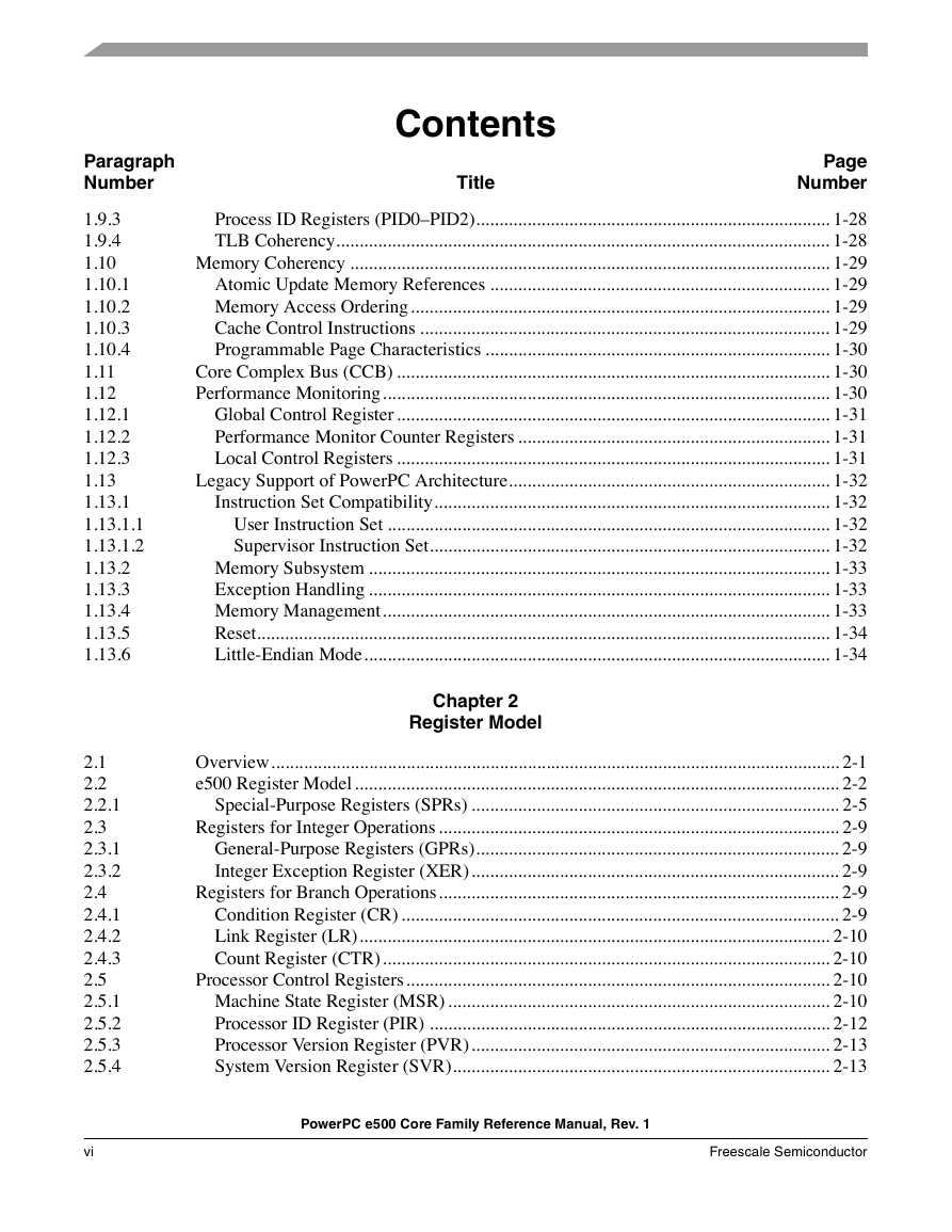
1.9.3 Process ID Registers (PID0-PID2)
1.9.4 TLB Coherency
1.10 Memory Coherency
1.10.1 Atomic Update Memory References
1.10.2 Memory Access Ordering
1.10.3 Cache Control Instructions
1.10.4 Programmable Page Characteristics
1.11 Core Complex Bus (CCB)
1.12 Performance Monitoring
1.12.1 Global Control Register
1.12.2 Performance Monitor Counter Registers
1.12.3 Local Control Registers
1.13 Legacy Support of PowerPC Architecture
1.13.1 Instruction Set Compatibility
1.13.1.1 User Instruction Set
1.13.1.2 Supervisor Instruction Set
1.13.2 Memory Subsystem
1.13.3 Exception Handling
1.13.4 Memory Management
1.13.5 Reset
1.13.6 Little-Endian Mode
Chapter 2 Register Model
2.1 Overview
2.2 e500 Register Model
Figure 2-1. e500 Register Model
2.2.1 Special-Purpose Registers (SPRs)
Table 2-1. Book E Special-Purpose Registers (by SPR Abbreviation)
Table 2-2. Implementation-Specific SPRs (by SPR Abbreviation)
2.3 Registers for Integer Operations
2.3.1 General-Purpose Registers (GPRs)
2.3.2 Integer Exception Register (XER)
2.4 Registers for Branch Operations
2.4.1 Condition Register (CR)
2.4.2 Link Register (LR)
2.4.3 Count Register (CTR)
2.5 Processor Control Registers
2.5.1 Machine State Register (MSR)
Figure 2-2. Machine State Register (MSR)
Table 2-3. MSR Field Descriptions
2.5.2 Processor ID Register (PIR)
2.5.3 Processor Version Register (PVR)
Figure 2-3. Processor Version Register (PVR)
Table 2-4. PVR Field Descriptions
2.5.4 System Version Register (SVR)
Figure 2-4. System Version Register (SVR)
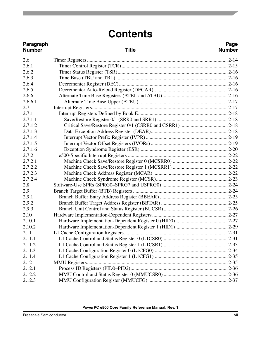
2.6 Timer Registers
Figure 2-5. Relationship of Timer Facilities to the Time Base
2.6.1 Timer Control Register (TCR)
Figure 2-6. Timer Control Register (TCR)
Table 2-5. TCR Implementation-Specific Field Descriptions
2.6.2 Timer Status Register (TSR)
2.6.3 Time Base (TBU and TBL)
2.6.4 Decrementer Register (DEC)
2.6.5 Decrementer Auto-Reload Register (DECAR)
2.6.6 Alternate Time Base Registers (ATBL and ATBU)
Figure 2-7. Alternate Time Base Register Lower (ATBL)
Table 2-6. ATBL Field Descriptions
2.6.6.1 Alternate Time Base Upper (ATBU)
Figure 2-8. Alternate Time Base Register Upper (ATBU)
Table 2-7. ATBU Field Descriptions
2.7 Interrupt Registers
2.7.1 Interrupt Registers Defined by Book E
2.7.1.1 Save/Restore Register 0/1 (SRR0 and SRR1)
2.7.1.2 Critical Save/Restore Register 0/1 (CSRR0 and CSRR1)
2.7.1.3 Data Exception Address Register (DEAR)
2.7.1.4 Interrupt Vector Prefix Register (IVPR)
2.7.1.5 Interrupt Vector Offset Registers (IVORs)
Figure 2-9. Interrupt Vector Offset Registers (IVORs)
Table 2-8. IVOR Assignments
2.7.1.6 Exception Syndrome Register (ESR)
Figure 2-10. Exception Syndrome Register (ESR)
Table 2-9. ESR Field Descriptions
2.7.2 e500-Specific Interrupt Registers
2.7.2.1 Machine Check Save/Restore Register 0 (MCSRR0)
Figure 2-11. Machine Check Save/Restore Register 0 (MCSRR0)
2.7.2.2 Machine Check Save/Restore Register 1 (MCSRR1)
Figure 2-12. Machine Check Save/Restore Register 1 (MCSRR1)
2.7.2.3 Machine Check Address Register (MCAR)
Figure 2-13. Machine Check Address Register (MCAR)
2.7.2.4 Machine Check Syndrome Register (MCSR)
Figure 2-14. Machine Check Syndrome Register (MCSR)
Table 2-10. MCSR Field Descriptions
2.8 Software-Use SPRs (SPRG0-SPRG7 and USPRG0)
2.9 Branch Target Buffer (BTB) Registers
2.9.1 Branch Buffer Entry Address Register (BBEAR)
Figure 2-15. Branch Buffer Entry Address Register (BBEAR)
Table 2-11. BBEAR Field Descriptions
2.9.2 Branch Buffer Target Address Register (BBTAR)
Figure 2-16. Branch Buffer Target Address Register (BBTAR)
Table 2-12. BBTAR Field Descriptions
2.9.3 Branch Unit Control and Status Register (BUCSR)
Figure 2-17. Branch Unit Control and Status Register (BUCSR)
Table 2-13. BUCSR Field Descriptions
2.10 Hardware Implementation-Dependent Registers
2.10.1 Hardware Implementation-Dependent Register 0 (HID0)
Figure 2-18. Hardware Implementation-Dependent Register 0 (HID0)
Table 2-14. HID0 Field Descriptions
2.10.2 Hardware Implementation-Dependent Register 1 (HID1)
Figure 2-19. Hardware Implementation-Dependent Register 1 (HID1)
Table 2-15. HID1 Field Descriptions
2.11 L1 Cache Configuration Registers
2.11.1 L1 Cache Control and Status Register 0 (L1CSR0)
Figure 2-20. L1 Cache Control and Status Register 0 (L1CSR0)
Table 2-16. L1CSR0 Field Descriptions
2.11.2 L1 Cache Control and Status Register 1 (L1CSR1)
Figure 2-21. L1 Cache Control and Status Register 1 (L1CSR1)
Table 2-17. L1CSR1 Field Descriptions
2.11.3 L1 Cache Configuration Register 0 (L1CFG0)
Figure 2-22. L1 Cache Configuration Register 0 (L1CFG0)
Table 2-18. L1CFG0 Field Descriptions
2.11.4 L1 Cache Configuration Register 1 (L1CFG1)
Figure 2-23. L1 Cache Configuration Register 1 (L1CFG1)
Table 2-19. L1CFG1 Field Descriptions
2.12 MMU Registers
2.12.1 Process ID Registers (PID0-PID2)
Figure 2-24. Process ID Registers (PID0-PID2)
2.12.2 MMU Control and Status Register 0 (MMUCSR0)
Figure 2-25. MMU Control and Status Register 0 (MMUCSR0)
Table 2-20. MMUCSR0 Field Descriptions
2.12.3 MMU Configuration Register (MMUCFG)
Figure 2-26. MMU Configuration Register (MMUCFG)
Table 2-21. MMUCFG Field Descriptions
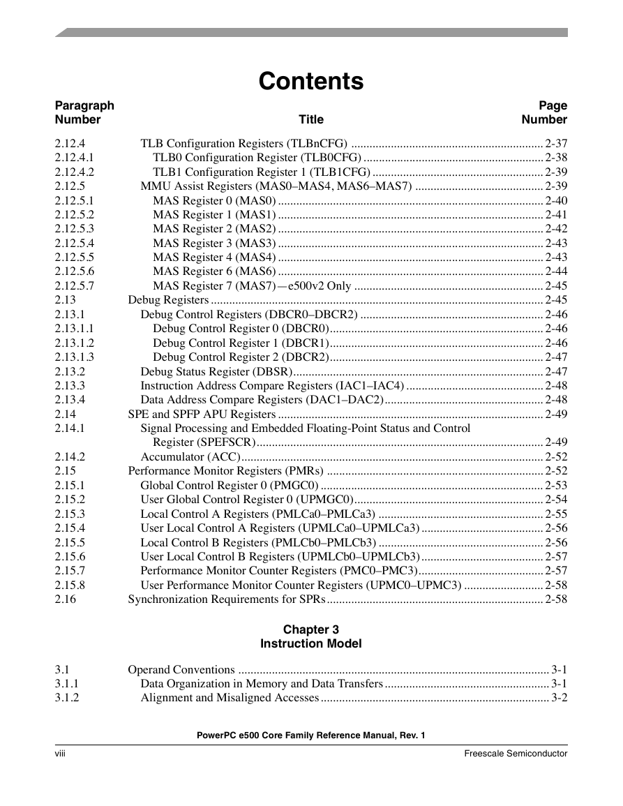
2.12.4 TLB Configuration Registers (TLBnCFG)
2.12.4.1 TLB0 Configuration Register (TLB0CFG)
Figure 2-27. TLB Configuration Register 0 (TLB0CFG)
Table 2-22. TLB0CFG Field Descriptions
2.12.4.2 TLB1 Configuration Register 1 (TLB1CFG)
Figure 2-28. TLB Configuration Register 1 (TLB1CFG)
Table 2-23. TLB1CFG Field Descriptions
2.12.5 MMU Assist Registers (MAS0-MAS4, MAS6-MAS7)
2.12.5.1 MAS Register 0 (MAS0)
Figure 2-29. MAS Register 0 (MAS0)
Table 2-24. MAS0 Field Descriptions-MMU Read/Write and Replacement Control
2.12.5.2 MAS Register 1 (MAS1)
Figure 2-30. MAS Register 1 (MAS1)
Table 2-25. MAS1 Field Descriptions-Descriptor Context and Configuration Control
2.12.5.3 MAS Register 2 (MAS2)
Figure 2-31. MAS Register 2 (MAS2)
Table 2-26. MAS2 Field Descriptions-EPN and Page Attributes
2.12.5.4 MAS Register 3 (MAS3)
Figure 2-32. MAS Register 3 (MAS3)
Table 2-27. MAS3 Field Descriptions-RPN and Access Control
2.12.5.5 MAS Register 4 (MAS4)
Figure 2-33. MAS Register 4 (MAS4)
Table 2-28. MAS4 Field Descriptions-Hardware Replacement Assist Configuration
2.12.5.6 MAS Register 6 (MAS6)
Figure 2-34. MAS Register 6 (MAS6)
Table 2-29. MAS6 Field Descriptions
2.12.5.7 MAS Register 7 (MAS7)-e500v2 Only
Figure 2-35. MAS Register 7 (MAS7)
Table 2-30. MAS7 Field Descriptions-High-Order RPN
2.13 Debug Registers
2.13.1 Debug Control Registers (DBCR0-DBCR2)
2.13.1.1 Debug Control Register 0 (DBCR0)
Table 2-31. DBCR0 Field Descriptions
2.13.1.2 Debug Control Register 1 (DBCR1)
Table 2-32. DBCR1 Implementation-Specific Field Descriptions
2.13.1.3 Debug Control Register 2 (DBCR2)
Figure 2-36. Debug Control Register 2 (DBCR2)
Table 2-33. DBCR2 Implementation-Specific Field Descriptions
2.13.2 Debug Status Register (DBSR)
Figure 2-37. Debug Status Register (DBSR)
Table 2-34. DBSR Implementation-Specific Field Descriptions
2.13.3 Instruction Address Compare Registers (IAC1-IAC4)
2.13.4 Data Address Compare Registers (DAC1-DAC2)
2.14 SPE and SPFP APU Registers
2.14.1 Signal Processing and Embedded Floating-Point Status and Control Register (SPEFSCR)
Figure 2-38. Signal Processing and Embedded Floating-Point Status and Control Register (SPEFSCR)
Table 2-35. SPEFSCR Field Descriptions
2.14.2 Accumulator (ACC)
2.15 Performance Monitor Registers (PMRs)
Table 2-36. Performance Monitor Registers-Supervisor Level
Table 2-37. Performance Monitor Registers-User Level (Read-Only)
2.15.1 Global Control Register 0 (PMGC0)
Figure 2-39. Performance Monitor Global Control Register 0 (PMGC0)/ User Performance Monitor Global Control Register 0 (UPMGC0)
Table 2-38. PMGC0 Field Descriptions
2.15.2 User Global Control Register 0 (UPMGC0)
2.15.3 Local Control A Registers (PMLCa0-PMLCa3)
Figure 2-40. Local Control A Registers (PMLCa0-PMLCa3)/ User Local Control A Registers (UPMLCa0-UPMLCa3)
Table 2-39. PMLCa0-PMLCa3 Field Descriptions
2.15.4 User Local Control A Registers (UPMLCa0-UPMLCa3)
2.15.5 Local Control B Registers (PMLCb0-PMLCb3)
Figure 2-41. Local Control B Registers (PMLCb0-PMLCb3)/ User Local Control B Registers (UPMLCb0-UPMLCb3)
Table 2-40. PMLCb0-PMLCb3 Field Descriptions
2.15.6 User Local Control B Registers (UPMLCb0-UPMLCb3)
2.15.7 Performance Monitor Counter Registers (PMC0-PMC3)
Figure 2-42. Performance Monitor Counter Registers (PMC0-PMC3)/ User Performance Monitor Counter Registers (UPMC0-UPMC3)
Table 2-41. PMC0-PMC3 Field Descriptions
2.15.8 User Performance Monitor Counter Registers (UPMC0-UPMC3)
2.16 Synchronization Requirements for SPRs
Table 2-42. Synchronization Requirements for SPRs
Chapter 3 Instruction Model
3.1 Operand Conventions
3.1.1 Data Organization in Memory and Data Transfers
3.1.2 Alignment and Misaligned Accesses
Table 3-1. Address Characteristics of Aligned Operands
3.1.3 e500 Floating-Point Implementation
3.1.4 Unsupported Book E Instructions
Table 3-2. Unsupported Book E Instructions (32-Bit)
3.2 Instruction Set Summary
3.2.1 Classes of Instructions
3.2.2 Definition of Boundedly Undefined
3.2.3 Synchronization Requirements
Table 3-3. Data Access Synchronization Requirements
3.2.3.1 Synchronization Requirements for e500-Specific SPRs
Table 3-4. Synchronization Requirements for e500-Specific SPRs
Table 3-5. Instruction Fetch and/or Execution Synchronization Requirements
3.2.3.2 Synchronization with tlbwe and tlbivax Instructions
3.2.3.3 Context Synchronization
3.2.3.4 Execution Synchronization
3.2.3.5 Instruction-Related Interrupts
3.3 Instruction Set Overview
3.3.1 Book E User-Level Instructions
3.3.1.1 Integer Instructions
3.3.1.1.1 Integer Arithmetic Instructions
Table 3-6. Integer Arithmetic Instructions
3.3.1.1.2 Integer Compare Instructions
Table 3-7. Integer 32-Bit Compare Instructions (L = 0)
3.3.1.1.3 Integer Logical Instructions
Table 3-8. Integer Logical Instructions
3.3.1.1.4 Integer Rotate and Shift Instructions
Table 3-9. Integer Rotate Instructions
Table 3-10. Integer Shift Instructions
3.3.1.2 Load and Store Instructions
3.3.1.2.1 Self-Modifying Code
3.3.1.2.2 Integer Load and Store Address Generation
Figure 3-1. Register Indirect with Immediate Index Addressing for Integer Loads/Stores
Figure 3-2. Register Indirect with Index Addressing for Integer Loads/Stores
Figure 3-3. Register Indirect Addressing for Integer Loads/Stores
3.3.1.2.3 Integer Load Instructions
Table 3-11. Integer Load Instructions
3.3.1.2.4 Integer Store Instructions
Table 3-12. Integer Store Instructions
3.3.1.2.5 Integer Load and Store with Byte-Reverse Instructions
Table 3-13. Integer Load and Store with Byte-Reverse Instructions
3.3.1.2.6 Integer Load and Store Multiple Instructions
Table 3-14. Integer Load and Store Multiple Instructions
3.3.1.3 Branch and Flow Control Instructions
3.3.1.3.1 Conditional Branch Control
Table 3-15. BO Bit Descriptions
Table 3-16. BO Operand Encodings
3.3.1.3.2 Branch Instructions
Table 3-17. Branch Instructions
3.3.1.3.3 Condition Register Logical Instructions
Table 3-18. Condition Register Logical Instructions
3.3.1.3.4 Trap Instructions
Table 3-19. Trap Instructions
3.3.1.4 System Linkage Instruction
Table 3-20. System Linkage Instruction
3.3.1.5 Processor Control Instructions
3.3.1.5.1 Move to/from Condition Register Instructions
Table 3-21. Move to/from Condition Register Instructions
3.3.1.5.2 Move to/from Special-Purpose Register Instructions
Table 3-22. Move to/from Special-Purpose Register Instructions
Table 3-23. Book E Special-Purpose Registers (by SPR Abbreviation)
Table 3-24. Implementation-Specific SPRs (by SPR Abbreviation)
3.3.1.6 Memory Synchronization Instructions
Table 3-25. Memory Synchronization Instructions
3.3.1.6.1 mbar (MO = 1)
3.3.1.7 Atomic Update Primitives Using lwarx and stwcx.
3.3.1.7.1 Reservations
3.3.1.7.2 Forward Progress
3.3.1.7.3 Reservation Loss Due to Granularity
3.3.1.8 Memory Control Instructions
3.3.1.8.1 User-Level Cache Instructions
Table 3-26. User-Level Cache Instructions
3.3.2 Supervisor-Level Instructions
3.3.2.1 System Linkage Instructions
Table 3-27. System Linkage Instructions-Supervisor-Level
Table 3-28. Move to/from Machine State Register Instructions
3.3.2.2 Supervisor-Level Memory Control Instructions
3.3.2.2.1 Supervisor-Level Cache Instruction
Table 3-29. Supervisor-Level Cache Management Instruction
3.3.2.2.2 Supervisor-Level TLB Management Instructions
Table 3-30. TLB Management Instructions
3.3.3 Recommended Simplified Mnemonics
3.3.4 Book E Instructions with Implementation-Specific Features
Table 3-31. Implementation-Specific Instructions Summary
3.3.5 e500 Instructions
Table 3-32. e500-Specific Instructions (Except SPE and SPFP Instructions)
3.3.6 Context Synchronization
3.4 Memory Access Alignment Support
Table 3-33. Natural Alignment Boundaries for Extended Vector Instructions
3.5 Using msync and mbar to Order Memory Accesses
3.5.1 Lock Acquisition and Import Barriers
3.5.1.1 Acquire Lock and Import Shared Memory
3.5.1.2 Obtain Pointer and Import Shared Memory
3.5.1.3 Lock Release and Export Barriers
3.5.1.3.1 Export Shared Memory and Release Lock
3.5.1.3.2 Export Shared Memory and Release Lock using mbar (MO = 0)
3.5.2 Safe Fetch
3.6 Update Instructions
3.7 Memory Synchronization
3.8 EIS-Defined Instructions and APUs Implemented on the e500
3.8.1 SPE and Embedded Floating-Point APUs
Figure 3-4. SPE and Floating-Point APU GPR Usage
3.8.1.1 SPE Operands: Signed Fractions
3.8.1.2 SPE Integer and Fractional Operations
Figure 3-5. Integer and Fractional Operations
3.8.1.3 SPE APU Instructions
Table 3-34. SPE APU Vector Multiply Instruction Mnemonic Structure
Table 3-35. Mnemonic Extensions for Multiply-Accumulate Instructions
Table 3-36. SPE APU Vector Instructions
3.8.1.4 Embedded Floating-Point APU Instructions
Table 3-37. Vector and Scalar Floating-Point APU Instructions
3.8.2 Integer Select (isel) APU
Table 3-38. Integer Select APU Instruction
3.8.3 Performance Monitor APU
Table 3-39. Performance Monitor APU Instructions
Table 3-40. e500-Defined PMR Encodings
3.8.4 Cache Locking APU
Table 3-41. Cache Locking APU Instructions
3.8.5 Machine Check APU
Table 3-42. Machine Check APU Instruction
3.9 e500-Specific Instructions
3.9.1 Branch Target Buffer (BTB) Locking Instructions
Table 3-43. Branch Target Buffer (BTB) Instructions
3.10 Instruction Listing
Table 3-44. List of Instructions
Chapter 4 Execution Timing
4.1 Terminology and Conventions
4.2 Instruction Timing Overview
Figure 4-1. Instruction Flow Pipeline Diagram Showing Pipeline Stages
Figure 4-2. e500 Instruction Flow Diagram-Details
Figure 4-3. GPR Issue Queue (GIQ)
Figure 4-4. Execution Pipeline Stages and Events
Figure 4-5. Execution Stages
4.3 General Timing Considerations
4.3.1 General Instruction Flow
4.3.2 Instruction Fetch Timing Considerations
4.3.2.1 L1 and L2 TLB Access Times
4.3.2.2 Interrupts Associated with Instruction Fetching
4.3.2.3 Cache-Related Latency
4.3.3 Dispatch, Issue, and Completion Considerations
4.3.3.1 GPR and CR Rename Register Operation
4.3.3.2 LR and CTR Shadow (Speculative) Registers
4.3.3.3 Instruction Serialization
4.3.4 Interrupt Latency
4.3.5 Memory Synchronization Timing Considerations
4.3.5.1 msync Instruction Timing Considerations
4.3.5.2 mbar Instruction Timing Considerations
4.4 Execution
4.4.1 Branch Unit Execution
4.4.1.1 Branch Instructions and Completion
Figure 4-6. Branch Completion (LR/CTR Write-Back)
4.4.1.2 BTB Branch Prediction and Resolution
Figure 4-7. Updating Branch History
4.4.1.3 BTB Operations
Figure 4-8. Fetch Groups and Cache Line Alignment
Figure 4-9. Fetch Group Addresses
4.4.1.3.1 BTB Locking
4.4.1.3.2 BTB Locking APU Programming Model
4.4.1.3.3 BTB Operations Controlled by BUCSR
4.4.1.3.4 BTB Special Cases-Phantom Branches and Multiple Matches
4.4.2 Load/Store Unit Execution
4.4.2.1 Load/Store Unit Queueing Structures
Figure 4-10. Cache/Core Interface Unit Integration
Table 4-1. Load and Store Queues
4.4.3 Simple and Multiple Unit Execution
Table 4-2. The Effect of Operand Size on Divide Latency
4.4.3.1 MU Divide Execution
Figure 4-11. MU Divide Bypass Path (Showing an 11-Cycle Divide)
4.4.3.2 MU Floating-Point Execution
4.4.4 Load/Store Execution
4.4.4.1 Effect of Operand Placement on Performance
4.5 Memory Performance Considerations
4.6 Instruction Latency Summary
Table 4-3. Branch Operation Execution Latencies
Table 4-4. System Operation Instruction Execution Latencies
Table 4-5. Condition Register Logical Execution Latencies
Table 4-6. SU and MU PowerPC Instruction Execution Latencies
Table 4-7. LSU Instruction Latencies
Table 4-8. SPE and Embedded Floating-Point APU Instruction Latencies
4.7 Instruction Scheduling Guidelines
4.7.1 Fetch/Branch Considerations
4.7.1.1 Dynamic Prediction versus No Branch Prediction
4.7.1.1.1 Position-Independent Code
4.7.2 Dispatch Unit Resource Requirements
4.7.2.1 Dispatch Groupings
4.7.3 Issue Queue Resource Requirements
4.7.3.1 General Issue Queue (GIQ)
4.7.3.2 Branch Issue Queue (BIQ)
4.7.4 Completion Unit Resource Requirements
4.7.4.1 Completion Groupings
4.7.5 Serialization Effects
4.7.6 Execution Unit Considerations
4.7.6.1 SU Considerations
4.7.6.2 MU Considerations
4.7.6.3 LSU Considerations
4.7.6.3.1 Load/Store Interaction
4.7.6.3.2 Misalignment Effects
Table 4-9. Natural Alignment Boundaries for Extended Vector Instructions
4.7.6.3.3 Load Miss Pipeline
Table 4-10. Data Cache Miss, L2 Cache Hit Timing
Chapter 5 Interrupts and Exceptions
5.1 Overview
5.2 e500 Interrupt Definitions
Table 5-1. SPE APU Unavailable Interrupt Generation When MSR[SPE] = 0
5.2.1 Recoverability from Interrupts
5.3 Interrupt Registers
Table 5-2. Interrupt Registers Defined by the PowerPC Architecture
Table 5-3. Exception Syndrome Register (ESR) Definition
Table 5-4. Machine Check Syndrome Register (MCSR) Field Descriptions
5.4 Exceptions
5.5 Interrupt Classes
Table 5-5. Asynchronous and Synchronous Interrupts
5.5.1 Requirements for System Reset Generation
5.6 Interrupt Processing
5.7 Interrupt Definitions
Table 5-6. Interrupt and Exception Types
5.7.1 Critical Input Interrupt
Table 5-7. Critical Input Interrupt Register Settings
5.7.2 Machine Check Interrupt
Table 5-8. e500 Machine Check Exception Sources
Table 5-9. Machine Check Interrupt Settings
5.7.2.1 Core Complex Bus (CCB) and L1 Cache Machine Check Errors
Table 5-10. Parity Error Exception Scenarios
5.7.2.2 Cache Parity Error Injection
5.7.3 Data Storage Interrupt
Table 5-11. Data Storage Interrupt Exception Conditions
Table 5-12. Data Storage Interrupt Register Settings
5.7.4 Instruction Storage Interrupt
Table 5-13. Instruction Storage Interrupt Exception Conditions
Table 5-14. Instruction Storage Interrupt Register Settings
5.7.5 External Input Interrupt
Table 5-15. External Input Interrupt Register Settings
5.7.6 Alignment Interrupt
Table 5-16. Alignment Interrupt Register Settings
5.7.7 Program Interrupt
Table 5-17. Program Interrupt Exception Conditions
Table 5-18. Program Interrupt Register Settings
5.7.8 System Call Interrupt
Table 5-19. System Call Interrupt Register Settings
5.7.9 Decrementer Interrupt
Table 5-20. Decrementer Interrupt Register Settings
5.7.10 Fixed-Interval Timer Interrupt
Table 5-21. Fixed-Interval Timer Interrupt Register Settings
5.7.11 Watchdog Timer Interrupt
Table 5-22. Watchdog Timer Interrupt Register Settings
5.7.12 Data TLB Error Interrupt
Table 5-23. Data TLB Error Interrupt Exception Conditions
Table 5-24. Data TLB Error Interrupt Register Settings
Table 5-25. MMU Assist Register Field Updates for TLB Error Interrupts
5.7.13 Instruction TLB Error Interrupt
Table 5-26. Instruction TLB Error Interrupt Exception Conditions
Table 5-27. Instruction TLB Error Interrupt Register Settings
5.7.14 Debug Interrupt
Table 5-28. Debug Interrupt Register Settings
5.7.15 EIS-Defined Interrupts
5.7.15.1 SPE/Embedded Floating-Point APU Unavailable Interrupt
Table 5-29. SPE/Embedded Floating-Point APU Unavailable Interrupt Register Settings
5.7.15.2 Embedded Floating-Point Data Interrupt
Table 5-30. Embedded Floating-Point Data Interrupt Register Settings
5.7.15.3 Embedded Floating-Point Round Interrupt
Table 5-31. Embedded Floating-Point Round Interrupt Register Settings
5.8 Performance Monitor Interrupt
5.9 Partially Executed Instructions
5.10 Interrupt Ordering and Masking
5.10.1 Guidelines for System Software
Table 5-32. Operations to Avoid
5.10.2 Interrupt Order
5.11 Exception Priorities
5.11.1 e500 Exception Priorities
5.12 e500 Interrupt Latency
5.13 Guarded Load and Cache-Inhibited stwcx. Instructions
Chapter 6 Power Management
6.1 Overview
6.2 Power Management Signals
Table 6-1. Power Management Signals of Core Complex
6.3 Core and Integrated Device Power Management States
Figure 6-1. Core Power Management State Diagram
Table 6-2. Core Power States
6.4 Power Management Control Bits
Table 6-3. Core Power Management Control Bits
6.4.1 Software Considerations for Power Management
6.5 Power Management Protocol
Figure 6-2. Example Core Power Management Handshaking
6.6 Interrupts and Power Management
Chapter 7 Performance Monitor
7.1 Overview
7.2 Performance Monitor APU Registers
Table 7-1. Performance Monitor Registers-Supervisor Level
Table 7-2. Performance Monitor Registers-User Level (Read-Only)
7.2.1 Global Control Register 0 (PMGC0)
Figure 7-1. Performance Monitor Global Control Register 0 (PMGC0)/ User Performance Monitor Global Control Register 0 (UPMGC0)
Table 7-3. PMGC0 Field Descriptions
7.2.2 User Global Control Register 0 (UPMGC0)
7.2.3 Local Control A Registers (PMLCa0-PMLCa3)
Figure 7-2. Local Control A Registers (PMLCa0-PMLCa3)/ User Local Control A Registers (UPMLCa0-UPMLCa3)
Table 7-4. PMLCa0-PMLCa3 Field Descriptions
7.2.4 User Local Control A Registers (UPMLCa0-UPMLCa3)
7.2.5 Local Control B Registers (PMLCb0-PMLCb3)
Figure 7-3. Local Control B Registers (PMLCb0-PMLCb3)/ User Local Control B Registers (UPMLCb0-UPMLCb3)
Table 7-5. PMLCb0-PMLCb3 Field Descriptions
7.2.6 User Local Control B Registers (UPMLCb0-UPMLCb3)
7.2.7 Performance Monitor Counter Registers (PMC0-PMC3)
Figure 7-4. Performance Monitor Counter Registers (PMC0-PMC3)/ User Performance Monitor Counter Registers (UPMC0-UPMC3)
Table 7-6. PMC0-PMC3 Field Descriptions
7.2.8 User Performance Monitor Counter Registers (UPMC0-UPMC3)
7.3 Performance Monitor APU Instructions
Table 7-7. Performance Monitor APU Instructions
7.4 Performance Monitor Interrupt
7.5 Event Counting
7.5.1 Processor Context Configurability
Table 7-8. Processor States and PMLCa0-PMLCa3 Bit Settings
7.6 Examples
7.6.1 Chaining Counters
7.6.2 Thresholding
7.7 Event Selection
Table 7-9. Event Types
Table 7-10. Performance Monitor Event Selection
Chapter 8 Debug Support
8.1 Overview
8.2 Programming Model
8.2.1 Register Set
Table 8-1. Debug SPRs
8.2.2 Instruction Set
8.2.3 Debug Interrupt Model
Table 8-2. Debug Interrupt Register Settings
8.2.4 Deviations from the Book E Debug Model
Table 8-3. DBCR0 and DBSR Field Differences
8.2.5 Hardware Facilities
8.3 TAP Controller and Register Model
Figure 8-1. TAP Controller with Supported Registers
8.3.1 TAP Interface Signals
Table 8-4. TAP/IEEE/JTAG Interface Signal Summary
Table 8-5. JTAG Signal Details
8.4 Book E Debug Events
Table 8-6. Debug Events
8.4.1 Instruction Address Compare Debug Event
8.4.1.1 Instruction Address Compare User and Supervisor Modes
8.4.1.2 Effective Address Mode
8.4.1.3 Instruction Address Compare Mode
Table 8-7. Instruction Address Compare Modes
8.4.2 Data Address Compare Debug Event
8.4.2.1 Data Address Compare Read/Write Enable
8.4.2.2 Data Address Compare User/Supervisor Mode
8.4.2.3 Effective Address Mode
8.4.2.4 Data Address Compare (DAC) Mode
Table 8-8. Data Address Compare Modes
8.4.3 Trap Debug Event
8.4.4 Branch Taken Debug Event
8.4.5 Instruction Complete Debug Event
8.4.6 Interrupt Taken Debug Event
8.4.7 Return Debug Event
8.4.8 Unconditional Debug Event
Part II e500 Core Complex
Chapter 9 Timer Facilities
9.1 Timer Facilities
Figure 9-1. Relationship of Timer Facilities to Time Base
9.2 Timer Registers
9.3 The e500 Timer Implementation
9.3.1 Alternate Time Base APU
9.3.2 Performance Monitor Time Base Event
Chapter 10 Auxiliary Processing Units (APUs)
10.1 Overview
Figure 10-1. Vector and Floating-Point APUs
10.2 Branch Target Buffer (BTB) Locking APU
10.2.1 BTB Locking APU Programming Model
10.2.1.1 BTB Locking APU Instructions
Table 10-1. BTB Locking APU Instructions
10.2.1.2 BTB Locking APU Registers
10.3 Alternate Time Base APU
10.3.1 Programming Model
10.4 Double-Precision Floating-Point APU (e500 v2 Only)
10.4.1 Programming Model
10.4.2 Double-Precision Floating-Point APU Operations
10.4.2.1 Operational Modes
10.4.2.2 Floating-Point Data Formats
Figure 10-2. Floating-Point Data Format
10.4.2.3 Overflow and Underflow
10.4.3 Instruction Descriptions
10.4.4 Embedded Floating-Point Results Summary
10.4.5 Floating-Point Conversion Models
10.4.5.1 Common Functions
10.4.5.2 Convert from Double-Precision Floating-Point to Integer Word with Saturation
10.4.5.3 Convert to Double-Precision Floating-Point from Integer Word with Saturation
Chapter 11 L1 Caches
11.1 Overview
11.1.1 Block Diagram
Figure 11-1. Cache/Core Interface Unit Integration
11.1.1.1 Load/Store Unit (LSU)
11.1.1.1.1 Caching-Allowed Loads and the LSU
11.1.1.1.2 Store Queue
11.1.1.1.3 L1 Load Miss Queue (LMQ)
11.1.1.1.4 Data Line Fill Buffer (DLFB)
11.1.1.1.5 Data Write Buffer (DWB)
11.1.1.2 Instruction Unit
11.1.1.3 Core Interface Unit
11.2 L1 Cache Organization
11.2.1 L1 Data Cache Organization
Figure 11-2. L1 Data Cache Organization
11.2.2 L1 Instruction Cache Organization
Figure 11-3. L1 Instruction Cache Organization
11.2.3 L1 Cache Parity
11.2.4 Cache Parity Error Injection
11.3 Cache Coherency Support
11.3.1 Data Cache Coherency Model
Table 11-1. Cache Line State Definitions
Table 11-2. L1 Data Cache Coherency State Transitions
11.3.2 Instruction Cache Coherency Model
Table 11-3. L1 Instruction Cache Coherency State Transitions
11.3.3 Snoop Signaling
Table 11-4. Data Cache Snoop Coherency State Transitions
Table 11-5. Instruction Cache Snoop Coherency State Transitions
11.3.4 WIMGE Settings and Effect on L1 Caches
11.3.4.1 Write-Back Stores
11.3.4.2 Write-Through Stores
11.3.4.3 Caching-Inhibited Loads and Stores
11.3.4.4 Misaligned Accesses and the Endian (E) Bit
11.3.4.5 Speculative Accesses to Guarded Memory
11.3.5 Load/Store Operations
11.3.5.1 Performed Loads and Stores
11.3.5.2 Sequential Consistency of Memory Accesses
11.3.5.3 Enforcing Store Ordering with Respect to Loads
11.3.5.4 Atomic Memory References
11.4 L1 Cache Control
11.4.1 Cache Control Instructions
Table 11-6. Cache Instruction Comparison
Table 11-7. Failed Cache Events
11.4.2 L1 Instruction and Data Cache Enabling/Disabling
11.4.3 L1 Instruction and Data Cache Flash Invalidation
11.4.4 L1 Instruction and Data Cache Line Locking/Unlocking
11.4.4.1 Effects of Other Cache Instructions on Locked Lines
11.4.4.2 Flash Clearing of Lock Bits
11.5 L1 Data Cache Flushing
11.6 L1 Cache Operation
11.6.1 Cache Miss and Reload Operations
11.6.1.1 Data Cache Fills
11.6.1.2 Instruction Cache Fills
11.6.1.3 Cache Allocation on Misses
11.6.1.4 Store Miss Merging
11.6.1.5 Store Hit to a Data Cache Block Marked Shared
11.6.1.6 Data Cache Block Push Operation
11.6.2 L1 Cache Block Replacement
11.6.2.1 PLRU Replacement
Table 11-8. L1 PLRU Replacement Way Selection
Figure 11-4. PLRU Replacement Algorithm
11.6.2.2 PLRU Bit Updates
Table 11-9. PLRU Bit Update Rules
11.6.2.3 Cache Locking and PLRU
11.7 L2 Cache Support
11.7.1 Invalidating the L2 Cache after a Cache Tag Parity Error
11.7.2 L2 Locking
11.7.2.1 L2 Unlocking
11.7.2.2 L1 Overlock
Chapter 12 Memory Management Units
12.1 e500 MMU Overview
12.1.1 MMU Features
12.1.2 TLB Entry Maintenance Features
Table 12-1. TLB Maintenance Programming Model
12.2 Effective-to-Real Address Translation
Figure 12-1. Effective-to-Real Address Translation Flow (e500v1)
Figure 12-2. Effective-to-Real Address Translation Flow (e500v2)
12.2.1 Virtual Addresses with Three PID Registers
12.2.2 Variable-Sized Pages
Table 12-2. Page Sizes for L1VSPs and TLB1 (L2 MMU) on the e500 Core
12.2.3 Checking for TLB Entry Hit
Figure 12-3. Virtual Address and TLB-Entry Compare Process
12.2.4 Checking for Access Permissions
12.3 Translation Lookaside Buffers (TLBs)
Figure 12-4. Two-Level MMU Structure
Table 12-3. Index of TLBs
12.3.1 L1 TLB Arrays
Figure 12-5. L1 MMU TLB Organization
12.3.2 L2 TLB Arrays
Figure 12-6. L2 MMU TLB Organization-e500v1
Figure 12-7. L2 MMU TLB Organization-e500v2
12.3.2.1 IPROT Invalidation Protection in TLB1
12.3.2.2 Replacement Algorithms for L2 MMU
12.3.2.2.1 Round-Robin Replacement for TLB0-e500v1
Figure 12-8. Round Robin Replacement for TLB0-e500v1
12.3.2.2.2 Round-Robin Replacement for TLB0-e500v2
Figure 12-9. Round Robin Replacement for TLB0-e500v2
12.3.3 Consistency Between L1 and L2 TLBs
Figure 12-10. L1 MMU TLB Relationships with L2 TLBs
12.3.4 L1 and L2 TLB Access Times
12.3.5 The G Bit (of WIMGE)
12.3.6 TLB Entry Field Definitions
Table 12-4. TLB Entry Bit Definitions for e500
12.4 TLB Instructions-Implementation
12.4.1 TLB Read Entry (tlbre) Instruction
12.4.1.1 Reading Entries from the TLB1 Array
12.4.1.2 Reading Entries from the TLB0 Array
12.4.2 TLB Write Entry (tlbwe) Instruction
12.4.2.1 Writing to the TLB1 Array
12.4.2.2 Writing to the TLB0 Array
12.4.3 TLB Search (tlbsx) Instruction-Searching the TLB1 and TLB0 Arrays
12.4.4 TLB Invalidate (tlbivax) Instruction
Table 12-5. tlbivax EA Bit Definitions
12.4.4.1 TLB Selection for tlbivax Instruction
12.4.4.2 Invalidate All Address Encoding for tlbivax Instruction
12.4.4.3 TLB Invalidate Broadcast Enabling
12.4.5 TLB Synchronize (tlbsync) Instruction
12.5 TLB Entry Maintenance-Details
12.5.1 Automatic Updates-TLB Miss Exceptions
12.5.2 TLB Interrupt Routines
12.5.2.1 Permissions Violations (ISI, DSI) Interrupt Handlers
12.6 TLB States after Reset
Table 12-6. TLB1 Entry 0 Values after Reset
12.7 Core Complex MMU Registers
Table 12-7. Registers Used for MMU Functions
12.7.1 e500 MAS Registers
Figure 12-11. MAS Register 0 (MAS0)
Table 12-8. MAS0 Field Descriptions-MMU Read/Write and Replacement Control
Figure 12-12. MAS Register 1 (MAS1)
Table 12-9. MAS1 Field Descriptions-Descriptor Context and Configuration Control
Figure 12-13. MAS Register 2 (MAS2)
Table 12-10. MAS2 Field Descriptions-EPN and Page Attributes
Figure 12-14. MAS Register 3 (MAS3)
Table 12-11. MAS3 Field Descriptions-RPN and Access Control
Figure 12-15. MAS Register 4 (MAS4)
Table 12-12. MAS4 Field Descriptions-Hardware Replacement Assist Configuration
Figure 12-16. MAS Register 6 (MAS6)
Table 12-13. MAS6-TLB Search Context Register 0
12.7.1.1 MAS Register 7 (MAS7)
Figure 12-17. MAS Register 7 (MAS7)
Table 12-14. MAS7 Field Descriptions-High Order RPN
12.7.2 MAS Register Updates
Table 12-15. MMU Assist Register Field Updates
Chapter 13 Core Complex Bus (CCB)
13.1 Overview
Figure 13-1. CCB Interface Signals
13.2 Signal Summary
Table 13-1. Summary of Selected Internal Signals
13.3 Core Interface Behavior
13.3.1 Parity Specification
13.3.2 msync Operation and the Bus
13.3.3 mbar Operation and the Bus
13.4 Address Streaming Mode
13.5 L2 Cache Support
13.5.1 L2 Locking
13.5.2 L2 Unlocking
13.5.3 L1 Overlock
13.6 Reservation Management
13.7 Remote Atomic Status Monitoring
13.8 Proper Reporting of Bus Faults
Appendix A Programming Examples
A.1 Synchronization
A.1.1 Synchronization Primitives
A.1.1.1 Fetch and No-op
A.1.1.2 Fetch and Store
A.1.1.3 Fetch and Add
A.1.1.4 Fetch and AND
A.1.1.5 Test and Set
A.1.1.6 Compare and Swap
A.1.1.7 Notes
A.1.2 Lock Acquisition and Release
A.1.3 List Insertion
A.1.3.1 Notes
Appendix B Guidelines for 32-Bit Book E
B.1 64-Bit-Specific Book E Instructions
B.2 Registers on 32-Bit Book E Implementations
B.3 Addressing on 32-Bit Book E Implementations
B.4 TLB Fields on 32-bit Book E Implementations
B.5 32-Bit Book E Software Guidelines
B.5.1 32-Bit Instruction Selection
B.5.2 32-Bit Addressing
Appendix C Simplified Mnemonics for PowerPC Instructions
C.1 Overview
C.2 Subtract Simplified Mnemonics
C.2.1 Subtract Immediate
C.2.2 Subtract
C.3 Rotate and Shift Simplified Mnemonics
C.3.1 Operations on Words
C.4 Branch Instruction Simplified Mnemonics
C.4.1 Key Facts about Simplified Branch Mnemonics
C.4.2 Eliminating the BO Operand
C.4.3 Incorporating the BO Branch Prediction
C.4.4 The BI Operand-CR Bit and Field Representations
C.4.4.1 BI Operand Instruction Encoding
C.4.4.1.1 Specifying a CR Bit
C.4.4.1.2 The crS Operand
C.4.5 Simplified Mnemonics that Incorporate the BO Operand
C.4.5.1 Examples that Eliminate the BO Operand
C.4.6 Simplified Mnemonics that Incorporate CR Conditions (Eliminates BO and Replaces BI with crS)
C.4.6.1 Branch Simplified Mnemonics that Incorporate CR Conditions: Examples
C.4.6.2 Branch Simplified Mnemonics that Incorporate CR Conditions: Listings
C.5 Compare Word Simplified Mnemonics
C.6 Condition Register Logical Simplified Mnemonics
C.7 Trap Instructions Simplified Mnemonics
C.8 Simplified Mnemonics for Accessing SPRs
C.9 Recommended Simplified Mnemonics
C.9.1 No-Op (nop)
C.9.2 Load Immediate (li)
C.9.3 Load Address (la)
C.9.4 Move Register (mr)
C.9.5 Complement Register (not)
C.9.6 Move to Condition Register (mtcr)
C.10 EIS-Specific Simplified Mnemonics
C.10.1 Integer Select (isel)
C.10.2 SPE Mnemonics
C.11 Comprehensive List of Simplified Mnemonics
Appendix D Opcode Listings
D.1 Instructions (Binary) by Mnemonic
D.2 Instructions (Decimal and Hexadecimal) by Opcode
D.3 Instructions by Form
Appendix E Revision History
E.1 Major Changes From Revision 0 to Revision 1
Index



 2023年江西萍乡中考道德与法治真题及答案.doc
 2012年重庆南川中考生物真题及答案.doc
 2013年江西师范大学地理学综合及文艺理论基础考研真题.doc
 2020年四川甘孜小升初语文真题及答案I卷.doc
 2020年注册岩土工程师专业基础考试真题及答案.doc
 2023-2024学年福建省厦门市九年级上学期数学月考试题及答案.doc
 2021-2022学年辽宁省沈阳市大东区九年级上学期语文期末试题及答案.doc
 2022-2023学年北京东城区初三第一学期物理期末试卷及答案.doc
 2018上半年江西教师资格初中地理学科知识与教学能力真题及答案.doc
 2012年河北国家公务员申论考试真题及答案-省级.doc
 2020-2021学年江苏省扬州市江都区邵樊片九年级上学期数学第一次质量检测试题及答案.doc
 2022下半年黑龙江教师资格证中学综合素质真题及答案.doc