Software Spotlight
ECC Options for Improving NAND Device Reliability
ECC Options for Improving NAND Flash Memory Reliability
A Micron Software Engineer Highlights Hardware and Software ECC Solutions
By Marina Mariano
Micron Software Engineer
NAND Flash memory devices cover a wide range of applications that go beyond traditional
storage in USB flash devices, memory cards, and solid state drives. NAND is being used
more and more as support for server solutions, networking products, embedded systems,
and so forth. These segments require a high level of reliability that is in contrast with the
technology shrinking, which can be a source of data corruption in memory storage.
In addition to increasing densities and decreasing device sizes, Micron creates products that
are more reliable than traditional NAND devices, thanks to a wide range of solutions that
can be adapted to a variety of markets. The needs of embedded systems, in conjunction
with our standards for excellence, have made it possible to design products aimed at a
stable level of performance and reliability throughout their lifespan.
To achieve the challenging level of reliability required by markets like embedded devices
and mobile phones, Micron protects data integrity with the adoption of error correction code
(ECC) in a broad variety of memory solutions. ECC was initially used in RAM, but now adds
reliability to NAND devices. This article discusses some of the ECC solutions available.
Using ECC to Improve NAND Data Integrity
In this article, we discuss NAND Flash memory devices that use one of two memory cell
technologies. The first is single-level cell (SLC) NAND in which each cell contains one bit,
which can be a 0 or 1. The second is multilevel cell (MLC) NAND, which provides the ability
to store two bits in each cell (or more in some cases). The voltage threshold determines the
content of each cell, representing one of four possible values for the two bits.
SLC NAND provides better data endurance compared to the same density MLC NAND
because of the accuracy required for recognizing the four different thresholds. Both SLC and
MLC NAND require an ECC algorithm to ensure data integrity. However, the data in MLC
NAND needs a significantly more sophisticated correction scheme to obtain the same level
of integrity.
PDF: 09005aef848aca27/Source: 09005aef848aca46
Rev. C, 01/12
© 2012 Micron Technology, Inc. Micron and the Micron logo are trademarks of Micron Technology, Inc. All other trademarks are the
property of their respective owners. All information is provided on an “AS IS” basis, without warranties of any kind.
�
Software Spotlight
ECC Options for Improving NAND Device Reliability
Figure 1. ECC Bit Correction Requirements Trend for SLC and MLC NAND
ECC Algorithms for NAND
General definitions in ECC algorithms provide for both error detection and error correction.
Error detection techniques enable the detection of errors, while error correction provides the
ability to reconstruct the original data. The general idea behind detection and correction
code is to introduce a redundancy to the data message, enabling the algorithm to check
whether the stored data is correct. NAND devices provide an additional storage area (called
the spare area) to add further information to the contents of a page. Typically, management
data such as ECC redundancy code is stored in the spare area in NAND.
Introducing a redundancy means setting the distance between valid words of the message,
which is the significant part of the user data. For example, a distance up to 4 bits ensures
that a 1-bit error and a 2-bit error can be distinguished from each other so that message
contents can be recovered when up to 4-bit errors occur.
Among the ECC code types, linear codes are the most common because of their algebraic
structure. They are easier to describe, encode, and decode than nonlinear codes.
The most widely adopted code for 1-bit ECC is the Hamming code, which detects and
corrects data corruption during operation on SLC NAND devices with geometry of 70nm and
above. The Hamming algorithm is an industry-accepted method for error detection and
correction in many NAND-based applications. It can detect 2-bit errors and correct up to 1
bit.
As previously stated, MLC and SLC NAND with high levels of shrink geometry require a
more complex correction code. One family of cyclic codes is known as BCH codes. The
binary BCH codes were discovered around 1960 by Hocquenghem and independently by
Bose and Ray-Chaudhuri, whose names make up the algorithm’s acronym. Around the time
BCH codes first appeared in literature, Reed and Solomon published a work describing a
PDF: 09005aef848aca27/Source: 09005aef848aca46
Rev. C, 01/12
© 2012 Micron Technology, Inc. Micron and the Micron logo are trademarks of Micron Technology, Inc. All other trademarks are the
property of their respective owners. All information is provided on an “AS IS” basis, without warranties of any kind.
�
Software Spotlight
ECC Options for Improving NAND Device Reliability
subclass of these codes. Because of their error-correction capabilities, Reed-Solomon
codes can be used to improve the general reliability of MLC NAND, compact discs, and
other data storage equipment.
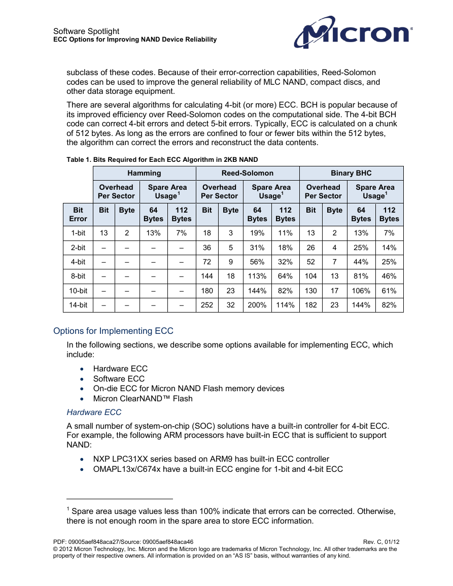
There are several algorithms for calculating 4-bit (or more) ECC. BCH is popular because of
its improved efficiency over Reed-Solomon codes on the computational side. The 4-bit BCH
code can correct 4-bit errors and detect 5-bit errors. Typically, ECC is calculated on a chunk
of 512 bytes. As long as the errors are confined to four or fewer bits within the 512 bytes,
the algorithm can correct the errors and reconstruct the data contents.
Table 1. Bits Required for Each ECC Algorithm in 2KB NAND
Bit
Error
1-bit
2-bit
4-bit
8-bit
10-bit
14-bit
Hamming
Reed-Solomon
Binary BHC
Overhead
Per Sector
Bit Byte
13
–
–
–
–
–
2
–
–
–
–
–
Spare Area
Usage1
64
Bytes
13%
–
–
–
–
–
112
Bytes
7%
–
–
–
–
–
Overhead
Per Sector
Bit Byte
18
36
72
144
180
252
3
5
9
18
23
32
Spare Area
Usage1
64
Overhead
Per Sector
Bit Byte
112
Bytes
11%
18%
32%
64%
82%
Bytes
13
19%
26
31%
52
56%
104
113%
144%
130
200% 114% 182
2
4
7
13
17
23
Spare Area
Usage1
64
Bytes
13%
25%
44%
81%
106%
144%
112
Bytes
7%
14%
25%
46%
61%
82%
Options for Implementing ECC
In the following sections, we describe some options available for implementing ECC, which
include:
Hardware ECC
Software ECC
On-die ECC for Micron NAND Flash memory devices
Micron ClearNAND™ Flash
Hardware ECC
A small number of system-on-chip (SOC) solutions have a built-in controller for 4-bit ECC.
For example, the following ARM processors have built-in ECC that is sufficient to support
NAND:
NXP LPC31XX series based on ARM9 has built-in ECC controller
OMAPL13x/C674x have a built-in ECC engine for 1-bit and 4-bit ECC
1 Spare area usage values less than 100% indicate that errors can be corrected. Otherwise,
there is not enough room in the spare area to store ECC information.
PDF: 09005aef848aca27/Source: 09005aef848aca46
Rev. C, 01/12
© 2012 Micron Technology, Inc. Micron and the Micron logo are trademarks of Micron Technology, Inc. All other trademarks are the
property of their respective owners. All information is provided on an “AS IS” basis, without warranties of any kind.
�
Software Spotlight
ECC Options for Improving NAND Device Reliability
The OMAP35x, AM35x, and AM/DM37x devices do not support 4-bit or 8-bit correction in
hardware. However, they do support 1-bit, 4-bit (excluding the OMAP35x), and 8-bit
hardware detection. It is important to note that using NAND that requires 8-bit ECC with 4-bit
hardware ECC could have negative consequences, including boot failure.
Software ECC
In the absence of hardware dedicated to calculating ECC, we have implemented a
Hamming code for 1-bit ECC and a multibit ECC encoder/decoder for NAND in software.
The library we provide to implement BCH ECC calculates the ECC on 512 bytes for NAND
sectors that consist of a 512-byte data area and a 16-byte spare area, totaling 528 bytes per
sector. A binary N-error-correcting BCH code is implemented to ensure data integrity (N
represents the number of bits that can be corrected). Inputs and outputs to or from the
encoder/decoder are in the byte format. Data is read out in two hex words per byte and the
information length of the BCH code must be a multiple of four. Even though the BCH
algorithm is designed for optimizing the implementation provided in software, 4-bit BCH
requires many microprocessor cycles to perform data computation.
ECC correction can be implemented in software for errors that are 2 bits and greater, and
optimized software can have good performance. However, the algorithm has a high
computational complexity and requires a large amount of RAM, which should be taken into
account when the code is implemented on embedded systems with limited resources.
On-Die ECC for Micron NAND Devices
Our MT29FxGxxAxxDAxx NAND is an example of a Micron device that provides built-in
ECC, which is tailored to ensure the highest level of reliability for each device. This device
includes a built-in 4-bit ECC internal controller. Although the adoption of a hardware
controller implies better READ speed performance when compared to an on-die ECC
implementation, the adoption of on-die ECC ensures smoother integration, and it is nearly
effortless for the user to replace existing memory devices. This means that
MT29FxGxxAxxDAxx devices can replace memory devices with 1-bit hardware support or
no hardware ECC support with only minor changes to the system. Enabling internal on-die
ECC ensures a high level of endurance for all types of Micron NAND family devices,
providing the user with a reliable memory solution.
Internal ECC enables 5-bit error detection and ensures 4-bit error correction. The on-die
ECC implements a BCH error correction code, and as a result, the number of partial page
programs cannot exceed four. Otherwise, the algorithm does not calculate the correction
code properly. During the busy time of the PROGRAM operation, the internal ECC
generates and stores the parity bit. Then, during a READ operation the on-die controller
checks for the presence of errors. When an error larger than four bits occurs, which cannot
be corrected, the engine signals the event and sets the least significant bit of the status
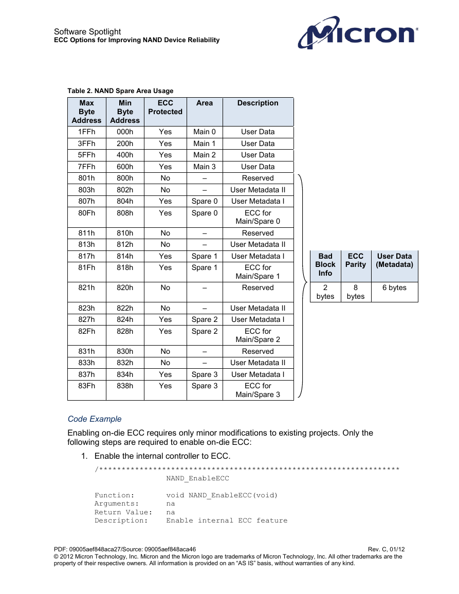
register. Results are unpredictable for errors that are 6 bits and greater. Table 2 illustrates
the usage of the NAND spare area with the limitation that a small part of the spare area is
not protected by ECC and the ECC user area must be included in the writing of four partial
pages.
PDF: 09005aef848aca27/Source: 09005aef848aca46
Rev. C, 01/12
© 2012 Micron Technology, Inc. Micron and the Micron logo are trademarks of Micron Technology, Inc. All other trademarks are the
property of their respective owners. All information is provided on an “AS IS” basis, without warranties of any kind.
�
Software Spotlight
ECC Options for Improving NAND Device Reliability
Table 2. NAND Spare Area Usage
ECC
Protected
Max
Byte
Min
Byte
Address
Address
1FFh
3FFh
5FFh
7FFh
801h
803h
807h
80Fh
811h
813h
817h
81Fh
821h
823h
827h
82Fh
831h
833h
837h
83Fh
000h
200h
400h
600h
800h
802h
804h
808h
810h
812h
814h
818h
820h
822h
824h
828h
830h
832h
834h
838h
Yes
Yes
Yes
Yes
No
No
Yes
Yes
No
No
Yes
Yes
No
No
Yes
Yes
No
No
Yes
Yes
Area
Description
Main 0
Main 1
Main 2
Main 3
–
–
Spare 0
Spare 0
–
–
Spare 1
Spare 1
–
–
Spare 2
Spare 2
–
–
Spare 3
Spare 3
User Data
User Data
User Data
User Data
Reserved
User Metadata II
User Metadata I
ECC for
Main/Spare 0
Reserved
User Metadata II
User Metadata I
ECC for
Main/Spare 1
Reserved
User Metadata II
User Metadata I
ECC for
Main/Spare 2
Reserved
User Metadata II
User Metadata I
ECC for
Main/Spare 3
Bad
Block
Info
2
bytes
ECC
Parity
User Data
(Metadata)
8
bytes
6 bytes
Code Example
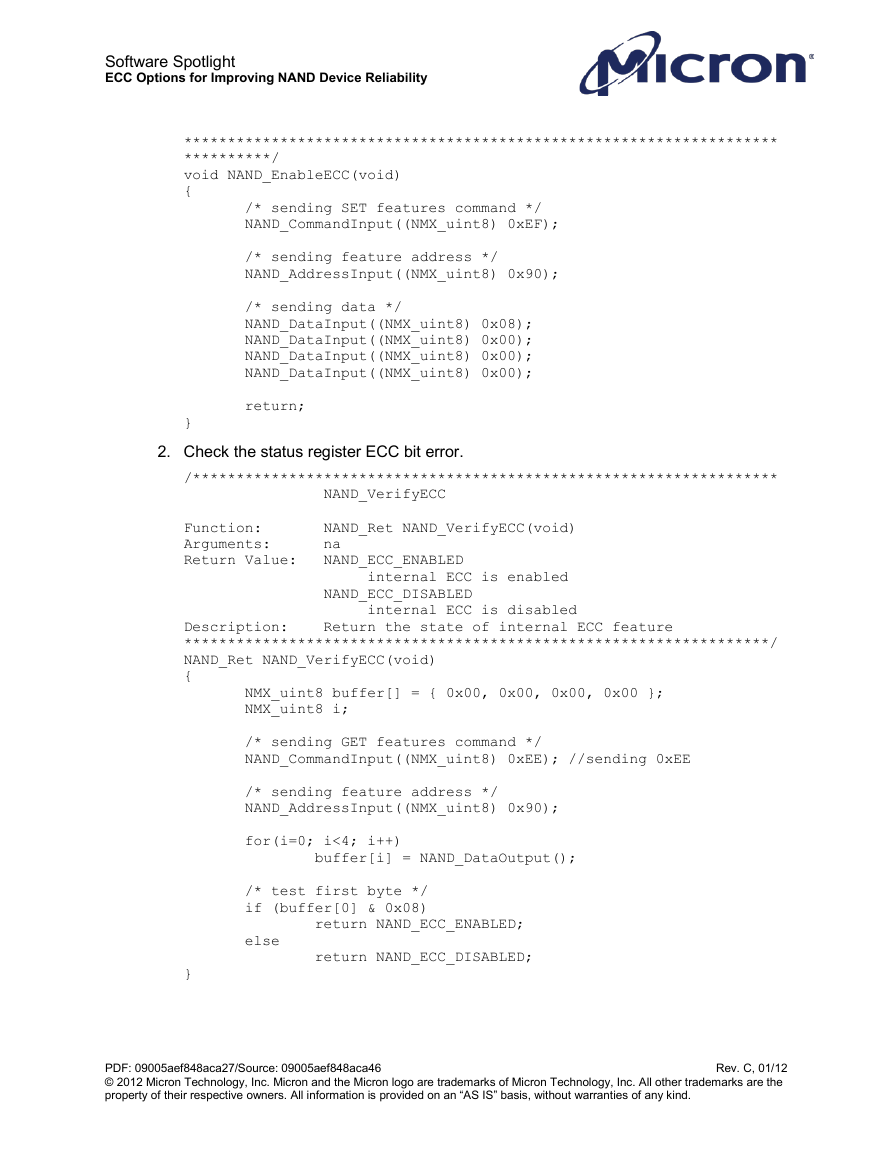
Enabling on-die ECC requires only minor modifications to existing projects. Only the
following steps are required to enable on-die ECC:
1. Enable the internal controller to ECC.
/*******************************************************************
NAND_EnableECC
Function: void NAND_EnableECC(void)
Arguments: na
Return Value: na
Description: Enable internal ECC feature
PDF: 09005aef848aca27/Source: 09005aef848aca46
Rev. C, 01/12
© 2012 Micron Technology, Inc. Micron and the Micron logo are trademarks of Micron Technology, Inc. All other trademarks are the
property of their respective owners. All information is provided on an “AS IS” basis, without warranties of any kind.
�
Software Spotlight
ECC Options for Improving NAND Device Reliability
********************************************************************
**********/
void NAND_EnableECC(void)
{
/* sending SET features command */
NAND_CommandInput((NMX_uint8) 0xEF);
/* sending feature address */
NAND_AddressInput((NMX_uint8) 0x90);
/* sending data */
NAND_DataInput((NMX_uint8) 0x08);
NAND_DataInput((NMX_uint8) 0x00);
NAND_DataInput((NMX_uint8) 0x00);
NAND_DataInput((NMX_uint8) 0x00);
return;
}
2. Check the status register ECC bit error.
/*******************************************************************
NAND_VerifyECC
Function: NAND_Ret NAND_VerifyECC(void)
Arguments: na
Return Value: NAND_ECC_ENABLED
internal ECC is enabled
NAND_ECC_DISABLED
internal ECC is disabled
Description: Return the state of internal ECC feature
*******************************************************************/
NAND_Ret NAND_VerifyECC(void)
{
NMX_uint8 buffer[] = { 0x00, 0x00, 0x00, 0x00 };
NMX_uint8 i;
/* sending GET features command */
NAND_CommandInput((NMX_uint8) 0xEE); //sending 0xEE
/* sending feature address */
NAND_AddressInput((NMX_uint8) 0x90);
for(i=0; i<4; i++)
buffer[i] = NAND_DataOutput();
/* test first byte */
if (buffer[0] & 0x08)
return NAND_ECC_ENABLED;
else
return NAND_ECC_DISABLED;
}
PDF: 09005aef848aca27/Source: 09005aef848aca46
Rev. C, 01/12
© 2012 Micron Technology, Inc. Micron and the Micron logo are trademarks of Micron Technology, Inc. All other trademarks are the
property of their respective owners. All information is provided on an “AS IS” basis, without warranties of any kind.
�
Software Spotlight
ECC Options for Improving NAND Device Reliability
ClearNAND Flash
ClearNAND Flash is our response to industry demands for a higher capacity solution that
also addresses existing ECC concerns. While we have been aggressively shrinking our
technology processes to meet those demands, we also recognize that process shrinks have
a direct effect on NAND performance and endurance and make error correction increasingly
difficult to manage. The adoption of an integrated solution for calculating ECC makes it
possible for users to develop one solution that can be easily migrated to future applications.
Our ClearNAND solution offers excellent performance in terms of throughput. For specific
applications, an effective Flash translation layer (FTL) solution should be adopted to
maximize the lifespan of the cells, even if this solution impacts overall performance.
Conclusion
As lithographies shrink, both SLC and MLC NAND increasingly require the use of ECC
algorithms to insure data integrity. Solutions include hardware, software, on-die, and
ClearNAND Flash. At Micron, we’ve developed a variety of ECC solutions for protecting data
integrity in a wide variety of applications. This means that we have the right NAND device
and ECC solution for every design. Micron’s NAND portfolio provides comprehensive, cost-
competitive memory products for computing, networking, mobile, and embedded
applications. For more information on our NAND and ECC solutions, contact your Micron
representative.”
References
TN-29-08: Hamming Codes for NAND Flash Memory Devices
TN-29-62: Software Device Drivers for Large Page Micron NAND Flash Memory
About the Author
Marina Mariano is a Micron software engineer responsible for
developing, debugging, and supporting software device drivers for
NAND, NOR, and phase change memory (PCM). She has been
instrumental in the development of low-level drivers for Micron.
PDF: 09005aef848aca27/Source: 09005aef848aca46
Rev. C, 01/12
© 2012 Micron Technology, Inc. Micron and the Micron logo are trademarks of Micron Technology, Inc. All other trademarks are the
property of their respective owners. All information is provided on an “AS IS” basis, without warranties of any kind.
�




 2023年江西萍乡中考道德与法治真题及答案.doc
 2012年重庆南川中考生物真题及答案.doc
 2013年江西师范大学地理学综合及文艺理论基础考研真题.doc
 2020年四川甘孜小升初语文真题及答案I卷.doc
 2020年注册岩土工程师专业基础考试真题及答案.doc
 2023-2024学年福建省厦门市九年级上学期数学月考试题及答案.doc
 2021-2022学年辽宁省沈阳市大东区九年级上学期语文期末试题及答案.doc
 2022-2023学年北京东城区初三第一学期物理期末试卷及答案.doc
 2018上半年江西教师资格初中地理学科知识与教学能力真题及答案.doc
 2012年河北国家公务员申论考试真题及答案-省级.doc
 2020-2021学年江苏省扬州市江都区邵樊片九年级上学期数学第一次质量检测试题及答案.doc
 2022下半年黑龙江教师资格证中学综合素质真题及答案.doc