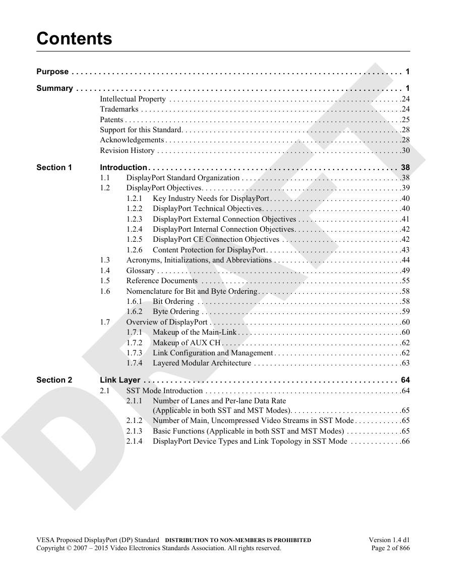
Contents
Tables
Figures
Preface
Intellectual Property
Trademarks
Patents
Support for this Standard
Acknowledgements
Revision History
1 Introduction
1.1 DisplayPort Standard Organization
1.2 DisplayPort Objectives
1.2.1 Key Industry Needs for DisplayPort
1.2.2 DisplayPort Technical Objectives
1.2.3 DisplayPort External Connection Objectives
1.2.4 DisplayPort Internal Connection Objectives
1.2.5 DisplayPort CE Connection Objectives
1.2.6 Content Protection for DisplayPort
1.3 Acronyms, Initializations, and Abbreviations
1.4 Glossary
1.5 Reference Documents
1.6 Nomenclature for Bit and Byte Ordering
1.6.1 Bit Ordering
1.6.1.1 Parallel Bit Ordering
1.6.1.2 Serial Bit Ordering after Channel Encoding
1.6.2 Byte Ordering
1.7 Overview of DisplayPort
1.7.1 Makeup of the Main-Link
1.7.2 Makeup of AUX CH
1.7.3 Link Configuration and Management
1.7.4 Layered Modular Architecture
2 Link Layer
2.1 SST Mode Introduction
2.1.1 Number of Lanes and Per-lane Data Rate (Applicable in both SST and MST Modes)
2.1.2 Number of Main, Uncompressed Video Streams in SST Mode
2.1.3 Basic Functions (Applicable in both SST and MST Modes)
2.1.4 DisplayPort Device Types and Link Topology in SST Mode
2.1.4.1 EDID and DPCD Access Handling by SST-only Mode Branch Devices
2.1.4.1.1 EDID and DPCD Access Handling by SST-only Replicator Device
2.1.4.1.2 EDID and DPCD Access Handling by SST-only Composite Sink Device (Informative)
2.1.4.2 Docking Station (Informative)
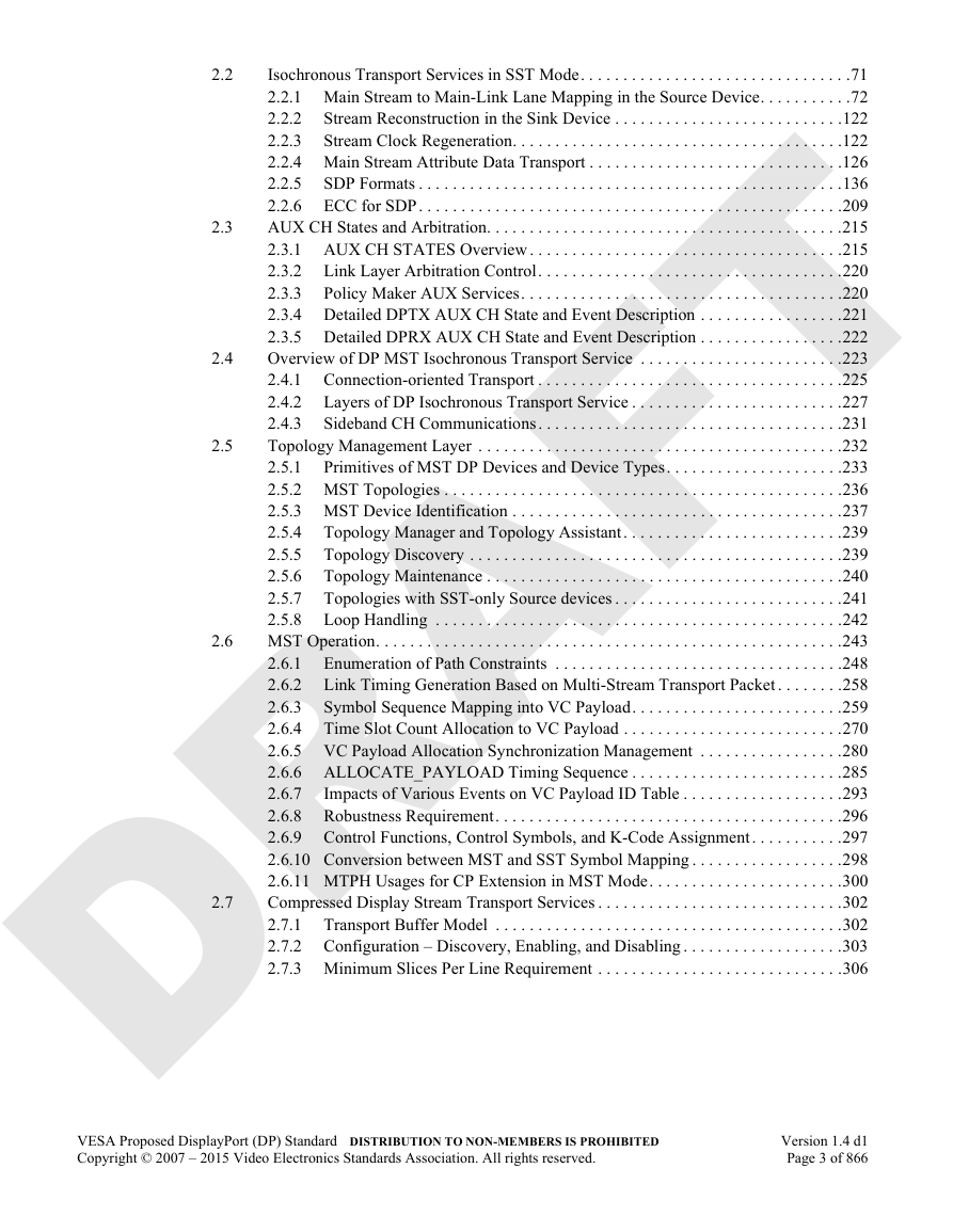
2.2 Isochronous Transport Services in SST Mode
2.2.1 Main Stream to Main-Link Lane Mapping in the Source Device
2.2.1.1 Default Framing Mode Control Symbols
2.2.1.2 Enhanced Framing Mode Control Symbols
2.2.1.3 Main Video Stream Data Packing
2.2.1.3.1 8bpc RGB/YCbCr 4:4:4 (24 bits per pixel)
2.2.1.3.2 6bpc RGB (18 bits per pixel)
2.2.1.3.3 10bpc RGB/YCbCr 4:4:4 (30 bits per pixel)
2.2.1.3.4 12bpc RGB/YCbCr 4:4:4 (36 bits per pixel)
2.2.1.3.5 16bpc RGB/YCbCr 4:4:4 (48 bits per pixel)
2.2.1.3.6 8bpc YCbCr 4:2:2 (16 bits per pixel)
2.2.1.3.7 10bpc YCbCr 4:2:2 (20 bits per pixel)
2.2.1.3.8 12bpc YCbCr 4:2:2 (24 bits per pixel)
2.2.1.3.9 16bpc YCbCr 4:2:2 (32 bits per pixel)
2.2.1.3.10 8bpc YCbCr 4:2:0 (12 bits per pixel)
2.2.1.3.11 10bpc YCbCr 4:2:0 (15 bits per pixel)
2.2.1.3.12 12bpc YCbCr 4:2:0 (18 bits per pixel)
2.2.1.3.13 16bpc YCbCr 4:2:0 (24 bits per pixel)
2.2.1.3.14 8bpp Y-only
2.2.1.3.15 10bpp Y-only
2.2.1.3.16 12bpp Y-only
2.2.1.3.17 16bpp Y-only
2.2.1.3.18 6bpp RAW
2.2.1.3.19 7bpp RAW
2.2.1.3.20 8bpp RAW
2.2.1.3.21 10bpp RAW
2.2.1.3.22 12bpp RAW
2.2.1.3.23 14bpp RAW
2.2.1.3.24 16bpp RAW
2.2.1.4 Symbol Stuffing and Transfer Unit
2.2.1.4.1 Transfer Unit Example (Informative)
2.2.1.4.2 Transfer Unit Generation with FEC Encoding/Decoding Enabled
2.2.1.5 Main Stream Attribute Packet/SDP Insertion
2.2.1.6 Inter-lane Skewing
2.2.2 Stream Reconstruction in the Sink Device
2.2.3 Stream Clock Regeneration
2.2.3.1 De-spreading of the Regenerated Stream Clock
2.2.3.2 DPRX Stream Clock Regeneration with FEC Encoding/Decoding Enabled
2.2.4 Main Stream Attribute Data Transport
2.2.4.1 Main Stream Attribute Secondary-data Packet Generation Options
2.2.4.1.1 Ignore MSA Video Timing Parameters (Ignore MSA) Option
2.2.4.1.2 Video Horizontal Blanking Expansion Option
2.2.4.1.2.1 Enabling Horizontal Blanking Expansion
2.2.4.1.2.2 DPRX Horizontal Blanking Expansion Capability Discovery
2.2.4.1.2.3 Horizontal Blanking Expansion Dependency on Buffer Size (Normative)
2.2.4.2 Main Stream Attribute for Interlaced Video Stream
2.2.4.3 Main Stream Attribute Field for Indication of Color Encoding Format and Content Color Gamut
2.2.5 SDP Formats
2.2.5.1 INFOFRAME SDP
2.2.5.1.1 INFOFRAME SDP Header v1.2
2.2.5.1.2 INFOFRAME SDP Header v1.3 and Payload
2.2.5.2 Audio_TimeStamp SDP
2.2.5.2.1 Audio_TimeStamp SDP Header
2.2.5.2.2 Audio_TimeStamp SDP Values (Informative)
2.2.5.3 Audio_Stream SDP
2.2.5.3.1 Audio Playback Latency Requirement
2.2.5.3.2 Audio_Stream SDP Header
2.2.5.3.3 Audio_Stream Data Mapping over the Main-Link
2.2.5.3.4 Audio_Stream SDP Splitting in SST Transport Format
2.2.5.3.5 Speaker Mapping
2.2.5.3.6 Data Mapping within Audio_Stream SDP Payload
2.2.5.3.7 Audio_Stream SDP Transport Capacity and Video Dependency (Informative)
2.2.5.3.8 Transport of Audio Packets without Main Video Stream
2.2.5.4 Audio_CopyManagement SDP
2.2.5.4.1 Audio_CopyManagement SDP Header
2.2.5.4.2 Audio_CopyManagement SDP Data
2.2.5.5 International Standard Recording Code SDP
2.2.5.5.1 ISRC SDP Header
2.2.5.5.2 ISRC SDP Data
2.2.5.6 Video_Stream_Configuration SDP
2.2.5.6.1 VSC SDP Header
2.2.5.6.2 VSC SDP Payload for 3D Stereo
2.2.5.6.3 VSC SDP Payload for PSR2
2.2.5.6.4 VSC SDP Payload for Pixel Encoding/Colorimetry Format
2.2.5.7 Extension SDP
2.2.5.7.1 Extension SDP Header
2.2.5.8 Camera SDP
2.2.5.8.1 Camera SDP Header
2.2.5.8.2 Camera SDP Transport (Informative)
2.2.5.9 Picture Parameter Set SDP
2.2.5.9.1 PPS SDP Header and Payload Bytes
2.2.5.10 Video Stream Configuration Extension VESA SDP
2.2.5.10.1 VSC_EXT_VESA and VSC_EXT_CEA SDP Header and Payload Bytes
2.2.5.11 Video Stream Configuration Extension CEA SDP
2.2.5.12 SDP Splitting in SST Mode
2.2.6 ECC for SDP
2.2.6.1 ECC Based on RS (15, 13)
2.2.6.2 ECC g1 and g0 C-code (Informative)
2.2.6.3 Nibble Interleaving
2.2.6.4 Corrective Action in the Event of Three Symbol Errors (Informative)
2.3 AUX CH States and Arbitration
2.3.1 AUX CH STATES Overview
2.3.1.1 Rules of DP_PWR State for a Source Device
2.3.1.2 Rules of DP_PWR State for a Sink Device
2.3.2 Link Layer Arbitration Control
2.3.3 Policy Maker AUX Services
2.3.4 Detailed DPTX AUX CH State and Event Description
2.3.5 Detailed DPRX AUX CH State and Event Description
2.4 Overview of DP MST Isochronous Transport Service
2.4.1 Connection-oriented Transport
2.4.2 Layers of DP Isochronous Transport Service
2.4.2.1 Topology Management Layer
2.4.2.2 Payload Bandwidth Management Layer
2.4.2.3 Link Management Layer
2.4.2.4 Main-Link Symbol Mapping Layer
2.4.2.5 VC Payload Mapping Layer
2.4.3 Sideband CH Communications
2.5 Topology Management Layer
2.5.1 Primitives of MST DP Devices and Device Types
2.5.1.1 Connection between Primitives: Physical Link and Logical Link
2.5.1.2 DP Branch Device
2.5.1.3 DP Source Device
2.5.1.4 DP Sink Device
2.5.1.5 DP Composite Device
2.5.2 MST Topologies
2.5.3 MST Device Identification
2.5.3.1 Global Unique Identifier
2.5.3.2 Relative Address
2.5.4 Topology Manager and Topology Assistant
2.5.4.1 Topology Manager
2.5.4.2 Topology Assistant
2.5.5 Topology Discovery
2.5.5.1 Topology Manager
2.5.5.2 Topology Assistant
2.5.6 Topology Maintenance
2.5.6.1 Topology Manager
2.5.6.2 Topology Assistant
2.5.7 Topologies with SST-only Source devices
2.5.8 Loop Handling
2.6 MST Operation
2.6.1 Enumeration of Path Constraints
2.6.1.1 Multi-function DP MST Branch Device Enumeration
2.6.1.1.1 Virtual DP Peer Device with DPCD Registers
2.6.1.1.2 DPCD Registers Relevant to Virtual DP Peer Devices
2.6.1.1.3 DSC Resource Management of DSC-capable Multi-function DP MST Branch Device
2.6.2 Link Timing Generation Based on Multi-Stream Transport Packet
2.6.2.1 MST Link Timing Generation with FEC Encoding/Decoding Enabled
2.6.3 Symbol Sequence Mapping into VC Payload
2.6.3.1 VC Payload Fill Symbol Sequence
2.6.3.2 Stream Symbol Sequence
2.6.3.2.1 Control Symbols
2.6.3.2.2 Data Symbols
2.6.3.3 SDP Transport in MST Mode
2.6.3.3.1 Number of Data Symbols Available for SDP Transport (Informative)
2.6.3.3.2 SDP Splitting in MST Mode
2.6.3.3.3 SDP-only Transport without Main Stream
2.6.3.3.4 No SDP/Main Stream
2.6.4 Time Slot Count Allocation to VC Payload
2.6.4.1 PBN Value Calculation by a Source Device Payload Bandwidth Manager
2.6.4.1.1 PBN Value Calculation with FEC Encoding/Decoding Enabled
2.6.4.2 VC Payload Size Determination by Branch Payload Bandwidth Manager
2.6.4.3 VC Payload Size Determination by a Source Payload Bandwidth Manager
2.6.4.3.1 Maximum Allowed Rate Governing Deviation from Target Average for a Source Device
2.6.4.3.2 Rate Governing Sample Pseudo-Code (Informative)
2.6.5 VC Payload Allocation Synchronization Management
2.6.6 ALLOCATE_PAYLOAD Timing Sequence
2.6.7 Impacts of Various Events on VC Payload ID Table
2.6.8 Robustness Requirement
2.6.8.1 Link Timing Robustness
2.6.8.2 Trigger Control Sequence Robustness in MTP Header Time Slot
2.6.8.3 VC Payload 4-Symbol Sequence Boundary Establishment
2.6.8.4 Stream Framing Symbol Sequence Robustness
2.6.9 Control Functions, Control Symbols, and K-Code Assignment
2.6.9.1 Control Functions
2.6.9.2 Control Symbol Index Scrambling
2.6.9.3 Data Symbol Scrambling
2.6.10 Conversion between MST and SST Symbol Mapping
2.6.10.1 Last Branch Device
2.6.10.1.1 Enablement of Enhanced Framing Symbol Sequence by the Last Branch Device
2.6.10.2 First Branch Device
2.6.10.2.1 Enhanced Framing Symbol Sequence support by the First Branch Device
2.6.10.3 Mode Switching between MST Mode and SST Mode
2.6.11 MTPH Usages for CP Extension in MST Mode
2.6.11.1 Encryption Control Field
2.6.11.2 Link Verification Pattern
2.6.11.3 Encryption of MTPH Time Slots
2.7 Compressed Display Stream Transport Services
2.7.1 Transport Buffer Model
2.7.2 Configuration – Discovery, Enabling, and Disabling
2.7.2.1 DP DSC Source Device
2.7.2.2 DP DSC Sink Device
2.7.3 Minimum Slices Per Line Requirement
2.7.3.1 Additional Slice per Display Line Options
2.7.3.2 Additional DP DSC Sink DSC Capabilities
2.7.3.3 Framing and Compressed Stream Mapping
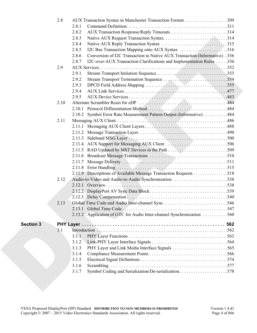
2.8 AUX Transaction Syntax in Manchester Transaction Format
2.8.1 Command Definition
2.8.1.1 Request Command Definition
2.8.1.2 Reply Command Definition
2.8.2 AUX Transaction Response/Reply Timeouts
2.8.3 Native AUX Request Transaction Syntax
2.8.3.1 Write Request Transactions
2.8.3.2 Read Request Transactions
2.8.4 Native AUX Reply Transaction Syntax
2.8.4.1 Reply Transaction to Write Request
2.8.4.2 Reply Transaction to a Read Request
2.8.5 I2C Bus Transaction Mapping onto AUX Syntax
2.8.5.1 I2C-over-AUX Request Transaction Command
2.8.5.2 I2C Write Transaction
2.8.5.3 I2C Read Transaction
2.8.5.4 I2C Write followed by I2C Read
2.8.6 Conversion of I2C Transaction to Native AUX Transaction (Informative)
2.8.7 I2C-over-AUX Transaction Clarifications and Implementation Rules
2.8.7.1 Clarifications for a Source Device
2.8.7.1.1 Downstream I2C Bit Rate Detection/Configuration
2.8.7.1.2 Prompting the Termination of I2C Transaction
2.8.7.1.3 MOT Bit
2.8.7.1.4 Prompting Repeated I2C Start Condition
2.8.7.1.5 I2C-write-over-AUX
2.8.7.1.5.1 Upon Receiving the Reply of I2C_ACK|AUX_ACK followed by no “M” Value to a Request Transaction with MOT Bit Cleared to 0
2.8.7.1.5.2 Upon Receiving the Reply of I2C_ACK|AUX_ACK followed by No “M” Value to a Request Transaction with MOT Bit Set to 1
2.8.7.1.5.3 Upon I2C_DEFER|AUX_ACK Reply, with MOT Bit in Request Transaction Cleared to 0 or Set to 1
2.8.7.1.5.4 Upon the Reply of I2C_ACK|AUX_ACK followed by “M” Value to the I2C-write-over-AUX, to a Request Transaction with MOT Bit Cleared to 0 or Set to 1
2.8.7.1.5.5 Upon Receiving I2C_NACK|AUX_ACK Reply followed by Either “M” Value or no “M” Value, to a Request Transaction with MOT Bit Cleared to 0 or Set to 1
2.8.7.1.5.6 Upon Receiving AUX_DEFER Reply to a Request Transaction with MOT Bit Cleared to 0 or Set to 1
2.8.7.1.5.6.1 Source Retry Attempts following AUX_DEFER Response prior to Aborting Transfer
2.8.7.1.5.7 Upon Receiving AUX_NACK Reply followed by Either “M” Value or no “M” Value
2.8.7.1.5.8 No Reply
2.8.7.1.6 I2C-read-over-AUX
2.8.7.1.6.1 Upon Receiving the Reply of I2C_ACK|AUX_ACK followed by the “Total” Number of Data Bytes Equal to LEN + 1, to a Request Transaction with MOT Bit Cleared to 0
2.8.7.1.6.2 Upon Receiving the Reply of I2C_ACK|AUX_ACK followed by the “Total” Number of Data Bytes Equal to LEN + 1 to a Request Transaction with MOT Bit Set to 1
2.8.7.1.6.3 Upon I2C_DEFER|AUX_ACK Reply, to a Request Transaction with MOT Bit Cleared to 0 or Set to 1
2.8.7.1.6.4 Upon the Reply of I2C_ACK|AUX_ACK followed by the Total Number of Data Bytes Fewer than LEN + 1, to a Request Transaction with MOT Bit Cleared to 0 or Set to 1
2.8.7.1.6.5 Upon Receiving I2C_NACK|AUX_ACK Reply to a Request Transaction with MOT Bit Cleared to 0 or Set to 1
2.8.7.1.6.6 Upon Receiving AUX_DEFER Reply to a Request Transaction with MOT Bit Cleared to 0 or Set to 1
2.8.7.1.6.6.1 Source Retry Attempts following AUX_DEFER Response prior to Aborting Transfer
2.8.7.1.6.7 No Reply
2.8.7.1.6.8 Clock Stretching
2.8.7.2 Clarifications for a Sink Device
2.8.7.2.1 I2C Bit Rate Capability Declaration and Setting
2.8.7.2.2 Termination/Completion of I2C Transaction
2.8.7.2.3 REPEATED I2C START Condition
2.8.7.2.4 I2C-write-over-AUX
2.8.7.2.4.1 I2C_ACK|AUX_ACK followed by No “M” Value
2.8.7.2.4.2 I2C_ACK|AUX_ACK followed by “M” Value
2.8.7.2.4.3 I2C_DEFER|AUX_ACK
2.8.7.2.4.4 I2C_NACK|AUX_ACK followed by Either “M” Value or No “M” Value
2.8.7.2.4.5 AUX_DEFER
2.8.7.2.4.6 AUX_NACK followed by Either “M” Value or No “M” Value
2.8.7.2.4.7 No Reply
2.8.7.2.5 I2C-read-over-AUX
2.8.7.2.5.1 I2C_ACK|AUX_ACK followed by the Total Number of Data Bytes Equal to LEN + 1
2.8.7.2.5.2 I2C_ACK|AUX_ACK followed by the Total Number of Bytes Fewer than LEN + 1
2.8.7.2.5.3 I2C_DEFER|AUX_ACK
2.8.7.2.5.4 I2C_NACK|AUX_ACK
2.8.7.2.5.5 AUX_DEFER
2.8.7.2.5.6 AUX_NACK
2.8.7.2.5.7 No Reply
2.8.7.2.6 Clock Stretching
2.8.7.3 Accessing EDID of More Than Two Blocks
2.9 AUX Services
2.9.1 Stream Transport Initiation Sequence
2.9.2 Stream Transport Termination Sequence
2.9.3 DPCD Field Address Mapping
2.9.3.1 DPCD Data Structure Revision Declaration
2.9.3.2 DPCD Field Address Mapping Tables
2.9.4 AUX Link Services
2.9.4.1 IEEE OUI and Device Identification
2.9.4.2 DPCD in Multi-Link Topology with SST-only Mode Source Device
2.9.4.2.1 Receiver Capability of Downstream Legacy Link
2.9.4.3 Link Initialization through Link Training
2.9.4.4 Link Maintenance
2.9.4.5 Link Quality Test Support
2.9.4.5.1 Transmission of Nyquist Pattern
2.9.4.5.2 Symbol Error Rate Measurement Pattern
2.9.4.5.3 PRBS and Bit Pattern
2.9.4.5.4 80-Bit Custom Pattern
2.9.4.5.5 CP2520 (HBR2 Compliance EYE Pattern)
2.9.5 AUX Device Services
2.9.5.1 E-DDC Support through I2C Mapping
2.9.5.2 MCCS over DDC/CI Support through I2C-over-AUX Transactions
2.9.5.3 Sink Event Notification
2.10 Alternate Scrambler Reset for eDP
2.10.1 Protocol Differentiation Method
2.10.2 Symbol Error Rate Measurement Pattern Output (Informative)
2.11 Messaging AUX Client
2.11.1 Messaging AUX Client Layers
2.11.2 Message Transaction Layer
2.11.2.1 Message Transaction Protocol
2.11.2.2 Message_Transaction_Request ()
2.11.2.2.1 Request_Identifier
2.11.2.2.2 Request_Data ()
2.11.2.3 Message_Transaction_Reply ()
2.11.2.3.1 Reply_Type
2.11.2.3.2 Request_Identifier
2.11.2.3.3 Reply_Data ()
2.11.2.3.3.1 Global_Unique_Identifier
2.11.2.3.3.2 Reason_For_NAK
2.11.2.3.3.3 WRITE_FAILURE
2.11.2.3.3.4 INVALID_RAD
2.11.2.3.3.5 CRC_FAILURE
2.11.2.3.3.6 BAD_PARAM
2.11.2.3.3.7 DEFER
2.11.2.3.3.8 LINK_FAILURE
2.11.2.3.3.9 NO_RESOURCES
2.11.2.3.3.10 DPCD_FAIL
2.11.2.3.3.11 I2C_NAK
2.11.2.3.3.12 ALLOCATE_FAIL
2.11.2.3.3.13 NAK_Data
2.11.2.3.3.14 ACK_Data ()
2.11.2.4 Handling of Multiple Message Transaction Requests
2.11.3 Sideband MSG Layer
2.11.3.1 Sideband MSG Header ()
2.11.3.1.1 Link_Count_Total
2.11.3.1.2 Link_Count_Remaining
2.11.3.1.3 Relative_Address
2.11.3.1.4 Sideband_MSG_Body_Length
2.11.3.1.5 Start_Of_Message_Transaction
2.11.3.1.6 End_Of_Message_Transaction
2.11.3.1.7 Path_Message
2.11.3.1.8 Message_Sequence_No
2.11.3.1.9 Sideband_MSG_Header_CRC
2.11.3.2 Sideband_MSG_Body()
2.11.3.2.1 Sideband_MSG_Data
2.11.3.2.2 Sideband_MSG_Data_CRC
2.11.4 AUX Support for Messaging AUX Client
2.11.4.1 Messaging AUX Client DPCD Locations
2.11.4.1.1 MST_CAP Bit of the MSTM_CAP DPCD Location
2.11.4.1.2 UP_REQ_EN Bit of the MSTM_CTRL DPCD Location
2.11.4.1.3 DOWN_REP_MSG_RDY Bit of the DEVICE_SERVICE_IRQ_VECTOR DPCD Location
2.11.4.1.4 UP_REQ_MSG_RDY bit of the DEVICE_SERVICE_IRQ_VECTOR DPCD Location
2.11.4.1.5 DOWN_REQ Sideband MSG Buffer
2.11.4.1.6 UP_REP Sideband MSG Buffer
2.11.4.1.7 DOWN_REP Sideband MSG Buffer
2.11.4.1.8 UP_REQ Sideband MSG Buffer
2.11.5 RAD Updated by MST Devices in the Path
2.11.6 Broadcast Message Transactions
2.11.6.1 Broadcast Message Syntax
2.11.6.2 Broadcast Message Reply
2.11.7 Message Delivery
2.11.7.1 Message Originating Device
2.11.7.1.1 Down Request Message
2.11.7.1.2 Up Request Message
2.11.7.2 Message Forwarding Device (Forward and Execute if Path Message)
2.11.7.2.1 Down Request Message Transaction
2.11.7.2.2 Down Reply Message Transaction
2.11.7.2.3 Up Request Message Transaction
2.11.7.2.4 Up Reply Message Transaction
2.11.7.3 Message Targeted Device
2.11.7.3.1 Down Request Message
2.11.7.3.2 Up Request Message
2.11.8 Error Handling
2.11.8.1 Message Transaction Layer Error Handling
2.11.8.2 Sideband MSG Layer Error Handling
2.11.8.3 AUX Layer Error Handling for Sideband MSG
2.11.8.3.1 AUX Error Handling for Down Message Transactions
2.11.8.3.2 AUX Error Handling for Up Message Transactions
2.11.9 Descriptions of Available Message Transaction Requests
2.11.9.1 ALLOCATE_PAYLOAD
2.11.9.1.1 Port_Number
2.11.9.1.2 Virtual_Channel_Payload_Identifier
2.11.9.1.3 Payload_Bandwidth_Number
2.11.9.1.4 Allocated_Payload_Bandwidth_Number
2.11.9.1.5 Number_SDP_Streams
2.11.9.1.6 SDP_Stream_Sink
2.11.9.2 CLEAR_PAYLOAD_ID_TABLE
2.11.9.3 CONNECTION_STATUS_NOTIFY
2.11.9.3.1 Global_Unique_Identifier
2.11.9.3.2 Port_Number
2.11.9.3.3 Legacy_Device_Plug_Status
2.11.9.3.4 DisplayPort_Device_Plug_Status
2.11.9.3.5 Messaging_Capability_Status
2.11.9.3.6 Input_Port
2.11.9.3.7 Peer_Device_Type
2.11.9.4 ENUM_PATH_RESOURCES
2.11.9.4.1 FEC_Capability
2.11.9.4.2 Full_Payload_Bandwidth_Number
2.11.9.4.3 Available_Payload_Bandwidth_Number
2.11.9.4.4 Port_Number
2.11.9.5 LINK_ADDRESS
2.11.9.5.1 Global_Unique_Identifier
2.11.9.5.2 Number_Of_Ports
2.11.9.5.3 Current_Capabilities_Structure
2.11.9.5.4 Input_Port
2.11.9.5.5 Peer_Device_Type
2.11.9.5.6 Port_Number
2.11.9.5.7 Messaging_Capability_Status
2.11.9.5.8 DisplayPort_Device_Plug_Status
2.11.9.5.9 Legacy_Device_Plug_Status
2.11.9.5.10 DPCD_Revision
2.11.9.5.11 Peer_Global_Unique_Identifier
2.11.9.5.12 Number_SDP_Streams
2.11.9.5.13 Number_SDP_Stream_Sinks
2.11.9.6 POWER_DOWN_PHY
2.11.9.6.1 Port_Number
2.11.9.7 POWER_UP_PHY
2.11.9.7.1 Port_Number
2.11.9.8 QUERY_PAYLOAD
2.11.9.8.1 Port_Number
2.11.9.8.2 Virtual_Channel_Payload_Identifier
2.11.9.8.3 Allocated_PBN
2.11.9.9 REMOTE_DPCD_READ
2.11.9.9.1 Port_Number
2.11.9.9.2 DPCD_Address
2.11.9.9.3 Number_Of_Bytes_To_Read
2.11.9.9.4 Number_Of_Bytes_Read
2.11.9.9.5 DPCD_Byte_Read
2.11.9.10 REMOTE_DPCD_WRITE
2.11.9.10.1 Port_Number
2.11.9.10.2 DPCD_Address
2.11.9.10.3 Number_Of_Bytes_To_Read
2.11.9.10.4 Number_Of_Bytes_To_Write
2.11.9.10.5 DPCD_Byte_To_Write
2.11.9.10.6 Number_Of_Bytes_Written_Before_Failure
2.11.9.10.7 Global_Unique_Identifier
2.11.9.11 REMOTE_I2C_READ
2.11.9.11.1 Number_Of_I2C_Write_Transactions
2.11.9.11.2 Port_Number
2.11.9.11.3 Write_I2C_Device_Identifier
2.11.9.11.4 Number_Of_Bytes_To_Write
2.11.9.11.5 I2C_Data_To_Write
2.11.9.11.6 No_Stop_Bit
2.11.9.11.7 I2C_Transaction_Delay
2.11.9.11.8 Read_I2C_Device_Identifier
2.11.9.11.9 Number_Of_Bytes_To_Read
2.11.9.11.10 Number_Of_Bytes_Read
2.11.9.11.11 I2C_Device_Byte_Read
2.11.9.11.12 Global_Unique_Identifer
2.11.9.11.13 Reason_For_NAK
2.11.9.11.14 I2C_NAK_Transaction
2.11.9.12 REMOTE_I2C_WRITE
2.11.9.12.1 Port_Number
2.11.9.12.2 Write_I2C_Device_Identifier
2.11.9.12.3 Number_Of_Bytes_To_Write
2.11.9.13 RESOURCE_STATUS_NOTIFY
2.11.9.13.1 Global_Unique_Identifier
2.11.9.13.2 Port_Number
2.11.9.13.3 Avaliable_PBN
2.11.9.13.4 SINK_EVENT_NOTIFY
2.11.9.13.5 QUERY_STREAM_ENCRYPTION_STATUS
2.12 Audio-to-Video and Audio-to-Audio Synchronization
2.12.1 Overview
2.12.2 DisplayPort AV Sync Data Block
2.12.3 Delay Compensation
2.12.3.1 Audio Delay DPCD Register
2.12.3.2 AV Sync Delay Compensation
2.12.3.3 Audio-to-Audio Sync Delay Compensation
2.13 Global Time Code and Audio Inter-channel Sync
2.13.1 Global Time Code
2.13.1.1 GTC Accumulator Requirement
2.13.1.2 DPCD Fields for GTC
2.13.1.3 GTC Lock Acquisition and Maintenance between Adjacent DP Devices with Manchester Transaction Format
2.13.1.3.1 GTC Lock Acquisition/Maintenance Procedure When DPTX Is GTC Master
2.13.1.3.1.1 Lock Acquisition Phase
2.13.1.3.1.2 Phase Skew Offset at the End of Lock Acquisition Phase
2.13.1.3.1.3 Lock Maintenance Phase
2.13.1.3.2 GTC Lock Acquisition/Maintenance Procedure When DPRX Is GTC Master
2.13.1.3.2.1 Lock Acquisition Phase
2.13.1.3.2.2 Phase Skew Offset at the End of Lock Acquisition Phase
2.13.1.3.2.3 Lock Maintenance Phase
2.13.1.4 Selection of GTC Grand Master
2.13.1.4.1 Selection of GTC Grand Master When Multiple Source Devices Present
2.13.1.4.1.1 Disabling GTC Synchronization
2.13.1.4.1.2 Branch Device GTC Handling Requirements
2.13.1.4.1.3 Power Management while GTC Is in Use
2.13.2 Application of GTC for Audio Inter-channel Synchronization
2.13.2.1 Presentation Time
2.13.2.1.1 Dynamic Adjustment of Presentation Time
2.13.2.1.2 Presentation Time Insertion for Multi-Channel Audio
3 PHY Layer
3.1 Introduction
3.1.1 PHY Layer Functions
3.1.1.1 Hot Plug/Unplug Detection Circuitry
3.1.1.2 AUX Channel Circuitry
3.1.1.3 Main-Link Circuitry
3.1.2 Link-PHY Layer Interface Signals
3.1.2.1 Hot Plug/Unplug Detection
3.1.2.2 AUX Channel
3.1.2.3 Main-Link
3.1.3 PHY Layer and Link Media Interface Signals
3.1.3.1 DP_PWR / DP_PWR_RETURN
3.1.3.2 Hot Plug/Unplug Detection
3.1.3.3 AUX Channel
3.1.3.4 Main-Link
3.1.4 Compliance Measurement Points
3.1.4.1 Compliance Cable Models
3.1.4.2 Main-Link Compliance Configurations
3.1.4.2.1 HBR2 Compliance Configuration
3.1.4.2.2 HBR Compliance Configuration
3.1.4.2.3 RBR Compliance Configuration
3.1.4.3 AUX Channel Compliance Configurations
3.1.5 Electrical Signal Definitions
3.1.5.1 Definition of Differential Voltage
3.1.5.2 Voltage Swing and Pre-emphasis
3.1.6 Scrambling
3.1.7 Symbol Coding and Serialization/De-serialization
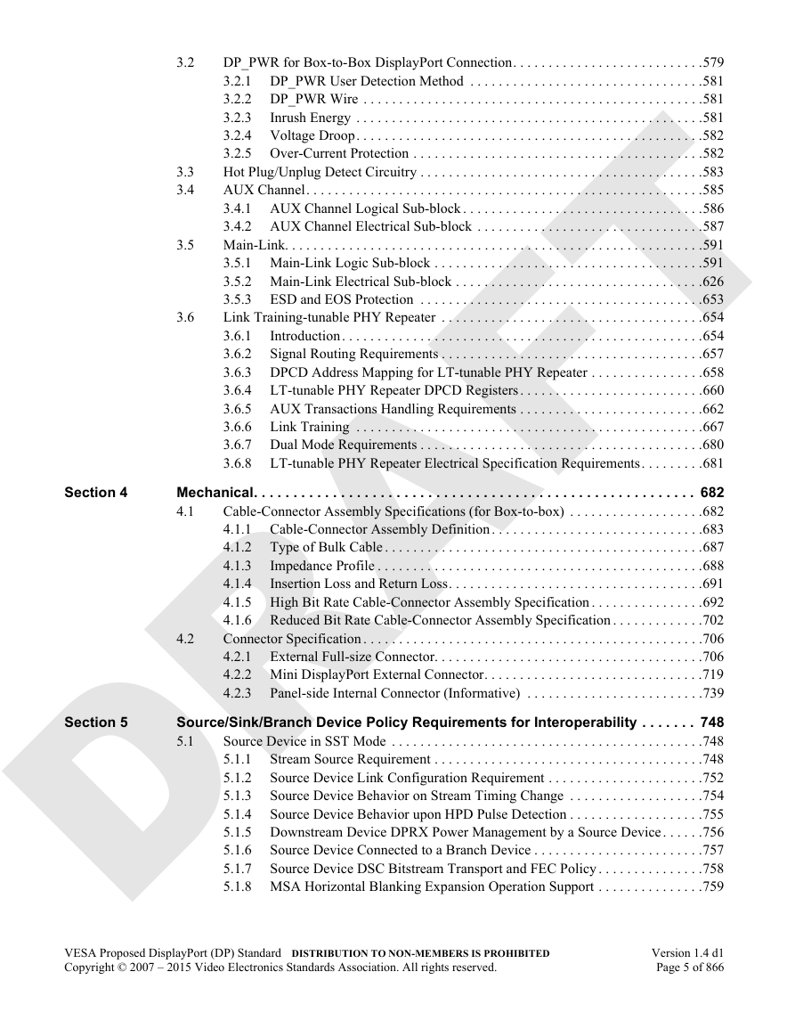
3.2 DP_PWR for Box-to-Box DisplayPort Connection
3.2.1 DP_PWR User Detection Method
3.2.2 DP_PWR Wire
3.2.3 Inrush Energy
3.2.4 Voltage Droop
3.2.4.1 DP_PWR Loss and Recovery on Branch Device
3.2.5 Over-Current Protection
3.3 Hot Plug/Unplug Detect Circuitry
3.4 AUX Channel
3.4.1 AUX Channel Logical Sub-block
3.4.2 AUX Channel Electrical Sub-block
3.4.2.1 AC-Coupling
3.4.2.2 Termination
3.4.2.3 DC Common Mode Voltage
3.4.2.4 Short Circuit Requirements
3.4.2.5 Differential Voltage/Timing (EYE) Diagram
3.5 Main-Link
3.5.1 Main-Link Logic Sub-block
3.5.1.1 ANSI 8b/10b Special Characters used for DP Control Link Symbols
3.5.1.2 Link Training
3.5.1.2.1 TPS4 Bit Sequence
3.5.1.2.2 Clock Recovery Sequence
3.5.1.2.2.1 Fallback Requirements in Case of Clock Recovery Failure on Lower-count Lanes
3.5.1.2.3 Channel Equalization Sequence
3.5.1.2.3.1 Fallback Requirements in Case of Symbol Lock Failures in 2- and 4-Lane Configurations
3.5.1.2.4 POST-LT_ADJ_REQ (Post-Link Training Adjust Request) Sequence
3.5.1.3 Link Maintenance
3.5.1.4 Link Quality Measurement (Testability)
3.5.1.5 RS (254, 250) FEC
3.5.1.5.1 FEC Encoding in DPTX
3.5.1.5.2 FEC Decoding in DPRX
3.5.1.5.3 RS(254, 250) FEC Polynomial and Test Vectors
3.5.1.5.4 Two-way Interleaving
3.5.1.5.5 Enabling/Disabling FEC Encoding/Decoding
3.5.1.5.6 DPCD Registers Used for FEC
3.5.1.5.7 DPCD Registers Used for FEC for LT-tunable Bit-level PHY Repeater
3.5.2 Main-Link Electrical Sub-block
3.5.2.1 AC-coupling
3.5.2.2 Termination
3.5.2.3 DC Common Mode Voltage
3.5.2.4 Short Circuit Requirements
3.5.2.5 Bandwidth of Transmitter/Receiver PLLs
3.5.2.6 Down-spreading of Link Clock
3.5.2.7 DisplayPort Jitter Specifications
3.5.2.7.1 Receiver Jitter Tolerance
3.5.2.7.1.1 HBR3 Receiver Jitter Tolerance
3.5.2.7.1.2 HBR2 Receiver Jitter Tolerance
3.5.2.7.1.3 HBR Receiver Jitter Tolerance
3.5.2.7.1.4 RBR Receiver Jitter Tolerance
3.5.2.7.2 Differential Noise Budget
3.5.2.8 Differential Voltage/Timing (EYE) Diagram
3.5.2.8.1 HBR3/HBR2 EYE Diagrams
3.5.2.8.2 HBR/RBR EYE Diagrams
3.5.2.9 Reference Equalizers
3.5.2.9.1 HBR3 Reference Equalizer
3.5.2.9.2 HBR3 Reference DFE
3.5.2.9.3 HBR2 Reference Equalizer
3.5.2.9.4 HBR Reference Equalizer
3.5.2.9.5 Enhanced HBR Reference Equalizer
3.5.2.10 Embedded Connection (Informative)
3.5.3 ESD and EOS Protection
3.6 Link Training-tunable PHY Repeater
3.6.1 Introduction
3.6.1.1 Two Data Path Types
3.6.1.2 Two Capability Types
3.6.1.3 Two Operating Modes
3.6.1.4 LT-tunable PHY Repeater Numbering for Multiple Repeaters between DPTX and DPRX
3.6.2 Signal Routing Requirements
3.6.3 DPCD Address Mapping for LT-tunable PHY Repeater
3.6.4 LT-tunable PHY Repeater DPCD Registers
3.6.4.1 LT-tunable PHY Repeater DPCD Capability and ID Field
3.6.4.2 LT-tunable PHY Repeater DPCD Link Configuration and Status Field(s)
3.6.5 AUX Transactions Handling Requirements
3.6.5.1 DPTX
3.6.5.2 DPRX
3.6.5.3 LT-tunable PHY Repeater
3.6.5.3.1 AUX Error Conditions
3.6.5.3.2 LT-tunable PHY Repeater AUX UFP (Informative)
3.6.5.3.3 LT-tunable PHY Repeater AUX DFP (Informative)
3.6.5.3.4 AUX Read Examples
3.6.5.3.5 AUX Write Examples
3.6.6 Link Training
3.6.6.1 DPTX Training Requirements
3.6.6.2 LT-Tunable PHY Repeater Training Requirements
3.6.6.3 Error Cases
3.6.6.4 Example Use Case
3.6.6.4.1 LT-tunable PHY Repeater Recognition
3.6.6.4.2 CR Phase with LT-tunable PHY Repeater2
3.6.6.4.3 LANEx_CR_DONE Phase with LT-tunable PHY Repeater1
3.6.6.4.4 CR Phase with DPRX
3.6.6.4.5 EQ Phase with LT-tunable PHY Repeater2
3.6.6.4.6 EQ Phase with LT-tunable PHY Repeater1
3.6.6.4.7 EQ Phase with DPRX
3.6.6.4.8 End of Link Training
3.6.7 Dual Mode Requirements
3.6.8 LT-tunable PHY Repeater Electrical Specification Requirements
3.6.8.1 LT-tunable PHY Repeater DPTX_PHY Electrical Compliance
3.6.8.2 LT-tunable PHY Repeater DPRX_PHY Electrical Compliance
4 Mechanical
4.1 Cable-Connector Assembly Specifications (for Box-to-box)
4.1.1 Cable-Connector Assembly Definition
4.1.1.1 Cable Construction Guideline for EMI Reduction (Informative)
4.1.2 Type of Bulk Cable
4.1.3 Impedance Profile
4.1.3.1 Impedance Profile through a DP Connector
4.1.3.2 Impedance Profile through an mDP Connector
4.1.4 Insertion Loss and Return Loss
4.1.5 High Bit Rate Cable-Connector Assembly Specification
4.1.5.1 Insertion Loss and Return Loss
4.1.5.1.1 Insertion Loss – Lower Limit for High Bit Rate Cable Assembly Type C1, C2, and C3
4.1.5.1.2 Insertion Loss – Lower Limit for High Bit Rate Resizing Adaptors
4.1.5.1.3 Insertion Loss – Lower Limit for Extension Cables
4.1.5.1.4 Return Loss – Upper Limit for HBR Cable Assembly/Adaptor (Full-sized DP Connector)
4.1.5.1.5 Return Loss – Upper Limit for HBR Cable Assembly/Adaptor/Extension Cable
4.1.5.2 Near End Noise
4.1.5.2.1 Near End Noise – Upper Limit for High Speed Cable Assembly
4.1.5.3 Power Sum Equal Level Far-End Noise
4.1.5.3.1 Power Sum Equal Level Far-End Noise – Upper Limit for High Speed Cable Assembly
4.1.5.4 Intra- and Inter-Pair Skew
4.1.5.4.1 Intra-Pair Skew
4.1.5.4.2 Inter-Pair Skew
4.1.6 Reduced Bit Rate Cable-Connector Assembly Specification
4.1.6.1 Insertion Loss and Return Loss
4.1.6.1.1 Insertion Loss – Lower Limit for Reduced Bit Rate Cable Assembly
4.1.6.1.2 Return Loss – Upper Limit for Reduced Bit Rate Cable Assembly
4.1.6.2 Near-End Noise
4.1.6.2.1 Near-End Noise – Upper Limit for Reduced Bit Rate Cable Assembly
4.1.6.3 Far-End Noise
4.1.6.4 Intra- and Inter-Pair Skew
4.1.6.4.1 Intra-Pair Skew
4.1.6.4.2 Inter-Pair Skew
4.2 Connector Specification
4.2.1 External Full-size Connector
4.2.1.1 Connector Pin Assignment
4.2.1.2 Contact Sequence
4.2.1.3 Connector Mechanical Performance
4.2.1.4 Connector Electrical Performance
4.2.1.5 Connector Environment Performance
4.2.1.6 Connector Performance Test Sequence
4.2.1.7 Connector Drawings
4.2.1.8 Cable Connector Drawings
4.2.1.9 Plug Overmold Dimensions for Non-Latch Plug Connector
4.2.1.10 Plug Connector and Board Connector Fully-Mated Condition
4.2.1.11 Recommended PCB Layout
4.2.1.12 Reference Design for Four DisplayPort External Connectors on a PCI Card
4.2.2 Mini DisplayPort External Connector
4.2.2.1 Mini DisplayPort Connector Pin Assignment
4.2.2.2 Mini DisplayPort Connector Mechanical Performance Requirements
4.2.2.3 Mini DisplayPort Connector Electrical Performance Requirements
4.2.2.4 Mini DisplayPort Connector Environmental Performance Requirements
4.2.2.5 Connector Performance Test Sequence
4.2.2.6 Mini DisplayPort Cable-Connector (Plug) Dimensions
4.2.2.7 Mini DisplayPort Connector (Receptacle) Dimensions
4.2.2.8 Mini DisplayPort Contact Sequence
4.2.2.9 Mini DisplayPort Panel Allowances
4.2.2.10 Recommended PCB Mounting
4.2.2.11 Reference Design for Four mDP Connectors on a Reduced Height PCI Card
4.2.3 Panel-side Internal Connector (Informative)
4.2.3.1 Panel-side Internal Connector Pin Assignment
4.2.3.2 Panel-side Internal Receptacle Connector
4.2.3.3 Panel-side Internal Plug Connector
4.2.3.4 Panel-side Internal Plug Connector – Contact and Mechanical Guide Details
4.2.3.5 Panel Side Connector Mechanical Requirements
4.2.3.6 Panel Side Connector Electrical Requirements
4.2.3.7 Panel Side Connector Environmental Requirements
5 Source/Sink/Branch Device Policy Requirements for Interoperability
5.1 Source Device in SST Mode
5.1.1 Stream Source Requirement
5.1.1.1 Video Colorimetry
5.1.1.1.1 RGB Colorimetry
5.1.1.1.2 YCbCr Colorimetry
5.1.1.1.3 Y-only Colorimetry
5.1.1.2 Video Timing Format
5.1.1.3 Audio Format
5.1.2 Source Device Link Configuration Requirement
5.1.2.1 Source Device Link Requirement when Other Interfaces are Supported
5.1.3 Source Device Behavior on Stream Timing Change
5.1.3.1 Video Stream Timing Change
5.1.3.2 Audio Stream Format/Timing Change
5.1.4 Source Device Behavior upon HPD Pulse Detection
5.1.5 Downstream Device DPRX Power Management by a Source Device
5.1.6 Source Device Connected to a Branch Device
5.1.7 Source Device DSC Bitstream Transport and FEC Policy
5.1.8 MSA Horizontal Blanking Expansion Operation Support
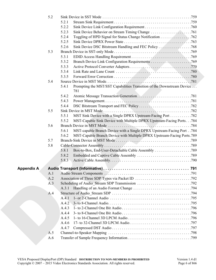
5.2 Sink Device in SST Mode
5.2.1 Stream Sink Requirement
5.2.1.1 Video Colorimetry
5.2.1.2 Video Timing Format
5.2.1.3 Audio Format
5.2.2 Sink Device Link Configuration Requirement
5.2.2.1 Sink Device Link Requirement when Other Interfaces are Supported
5.2.3 Sink Device Behavior on Stream Timing Change
5.2.3.1 Main Video Stream Timing Change
5.2.3.2 Audio Stream Format/Timing Change
5.2.4 Toggling of HPD Signal for Status Change Notification
5.2.5 Sink Device DPRX Power State
5.2.5.1 DP Sink Device Power State Specification Extensions
5.2.5.1.1 Extended Wake Timeout from SLEEP Power State
5.2.5.1.2 CONNECTED_OFF Power State
5.2.5.1.2.1 Entry into CONNECTED_OFF Power State
5.2.5.1.2.2 Exit from CONNECTED_OFF Power State
5.2.6 Sink Device DSC Bitstream Handling and FEC Policy
5.3 Branch Device in SST-only Mode
5.3.1 EDID Access Handling Requirement
5.3.2 Branch Device Link Configuration Requirements
5.3.2.1 Branch Device’s Power State Transition Handling
5.3.2.2 Branch Device DSC Bitstream Handling and FEC Policy
5.3.3 Active Protocol Converter Adaptors
5.3.3.1 General Requirements
5.3.3.2 VGA Protocol Converter Adaptors
5.3.3.3 DVI, HDMI, and DP++ Protocol Converter Adaptors
5.3.3.3.1 CEC-Tunneling-over-AUX
5.3.3.3.1.1 Terminologies
5.3.3.3.1.2 Overview
5.3.3.3.1.3 CEC-Tunneling-over-AUX Field
5.3.3.3.1.4 Power Management Considerations
5.3.3.4 S-Video/Composite/Other Analog Video Protocol Converter Adaptors
5.3.3.5 Dual-link DVI Protocol Converter Adaptors
5.3.3.6 MSA Horizontal Blanking Expansion Operation Support
5.3.4 Link Rate and Lane Count
5.3.5 Forward Error Correction
5.4 Source Device in MST Mode
5.4.1 Prompting the MST/SST Capabilities Transition of the Downstream Device
5.4.2 Atomic Message Transaction Generation
5.4.3 Power Management
5.4.4 DSC Bitstream Transport and FEC Policy
5.5 Sink Device in MST Mode
5.5.1 MST Sink Device with a Single DPRX Upstream-Facing Port
5.5.1.1 Transition to SST Mode
5.5.1.2 Transition to MST Mode
5.5.1.3 Issuance of Connection Status Notify Message Transactions
5.5.1.4 Issuance of Resource Status Notify Message Transactions
5.5.1.5 Power Management Handling
5.5.1.6 Mvid/Nvid and Maud/Naud Handling
5.5.1.7 Split SDP Handling
5.5.1.8 DSC Bitstream Handling and FEC
5.5.1.9 Interleaved Message Transactions Handling
5.5.2 MST-Capable Sink Device with Multiple DPRX Upstream-Facing Ports
5.6 Branch Device in MST Mode
5.6.1 MST-capable Branch Device with a Single DPRX Upstream-Facing Port
5.6.1.1 Transition to SST Mode
5.6.1.2 Transition to MST Mode
5.6.1.3 Issuance of Connection Status Notify Message Transactions
5.6.1.4 Issuance of Resource Status Notify Message Transactions
5.6.1.5 Power Management Handling
5.6.1.6 Multi-function MST Branch Device Enumeration
5.6.1.7 Mvid/Nvid and Maud/Naud Handling
5.6.1.8 Split SDP Handling
5.6.1.9 DSC Bitstream Handling and FEC
5.6.1.10 Interleaved Message Transactions Handling
5.6.2 MST-Capable Branch Device with Multiple DPRX Upstream-Facing Ports
5.7 Branch-Sink Device in MST Mode
5.8 Cable-Connector Assembly
5.8.1 Box-to-Box, End-User-Detachable Cable Assembly
5.8.2 Embedded and Captive Cable Assembly
5.8.3 Active Cable Assembly
5.8.3.1 Active Cable Assembly Electrical Parameters
5.8.3.2 Active Cable Assembly DP_PWR Requirements
A Audio Transport (Informative)
A.1 Audio Stream Components
A.2 Association of Three SDP Types via Packet ID
A.3 Scheduling of Audio_Stream SDP Transmission
A.3.1 Handling of an Audio Format Change
A.4 Structure of Audio_Stream SDP
A.4.1 1- or 2-Channel Audio
A.4.2 3- to 8-Channel Audio
A.4.3 1- to 2-Channel One Bit Audio
A.4.4 3- to 8-Channel One Bit Audio
A.4.5 1- to 16-Channel 3D LPCM Audio
A.4.6 17- to 32-Channel 3D LPCM Audio
A.4.7 Compressed DST Audio
A.5 Channel-to-Speaker Mapping
A.6 Transfer of Sample Frequency Information
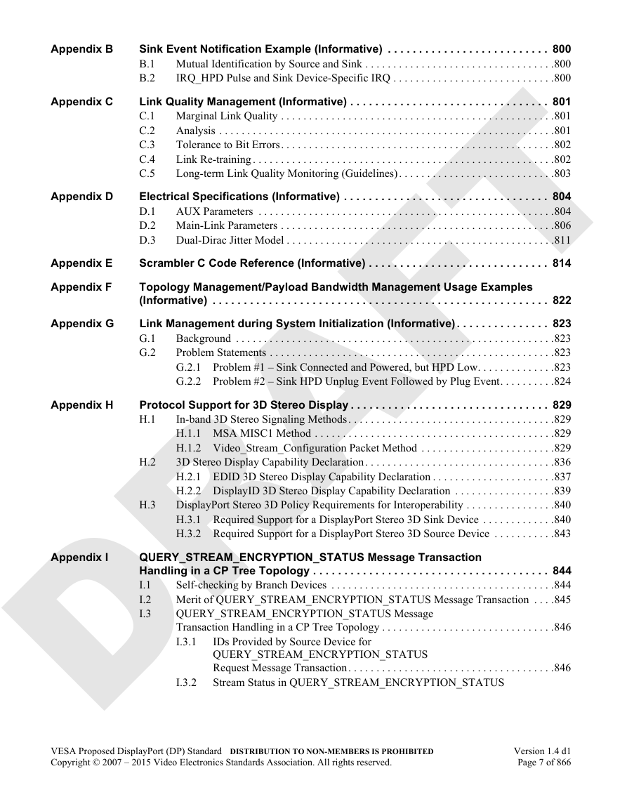
B Sink Event Notification Example (Informative)
B.1 Mutual Identification by Source and Sink
B.2 IRQ_HPD Pulse and Sink Device-Specific IRQ
C Link Quality Management (Informative)
C.1 Marginal Link Quality
C.2 Analysis
C.3 Tolerance to Bit Errors
C.4 Link Re-training
C.5 Long-term Link Quality Monitoring (Guidelines)
D Electrical Specifications (Informative)
D.1 AUX Parameters
D.2 Main-Link Parameters
D.3 Dual-Dirac Jitter Model
E Scrambler C Code Reference (Informative)
F Topology Management/Payload Bandwidth Management Usage Examples (Informative)
G Link Management during System Initialization (Informative)
G.1 Background
G.2 Problem Statements
G.2.1 Problem #1 – Sink Connected and Powered, but HPD Low
G.2.2 Problem #2 – Sink HPD Unplug Event Followed by Plug Event
H Protocol Support for 3D Stereo Display
H.1 In-band 3D Stereo Signaling Methods
H.1.1 MSA MISC1 Method
H.1.2 Video_Stream_Configuration Packet Method
H.1.2.1 VSC Packet Header
H.1.2.2 VSC Packet Payload
H.2 3D Stereo Display Capability Declaration
H.2.1 EDID 3D Stereo Display Capability Declaration
H.2.1.1 Side-by-Side Interleaved Stereo for Horizontally and Vertically Packed Formats
H.2.2 DisplayID 3D Stereo Display Capability Declaration
H.3 DisplayPort Stereo 3D Policy Requirements for Interoperability
H.3.1 Required Support for a DisplayPort Stereo 3D Sink Device
H.3.1.1 Stereo 3D Sink Field Sequential Mode
H.3.1.2 Stereo 3D Sink Stacked Top, Bottom Stereo Format
H.3.2 Required Support for a DisplayPort Stereo 3D Source Device
I QUERY_STREAM_ENCRYPTION_ STATUS Message Transaction Handling in a CP Tree Topology
I.1 Self-checking by Branch Devices
I.2 Merit of QUERY_STREAM_ENCRYPTION_STATUS Message Transaction
I.3 QUERY_STREAM_ENCRYPTION_STATUS Message Transaction Handling in a CP Tree Topology
I.3.1 IDs Provided by Source Device for QUERY_STREAM_ENCRYPTION_STATUS Request Message Transaction
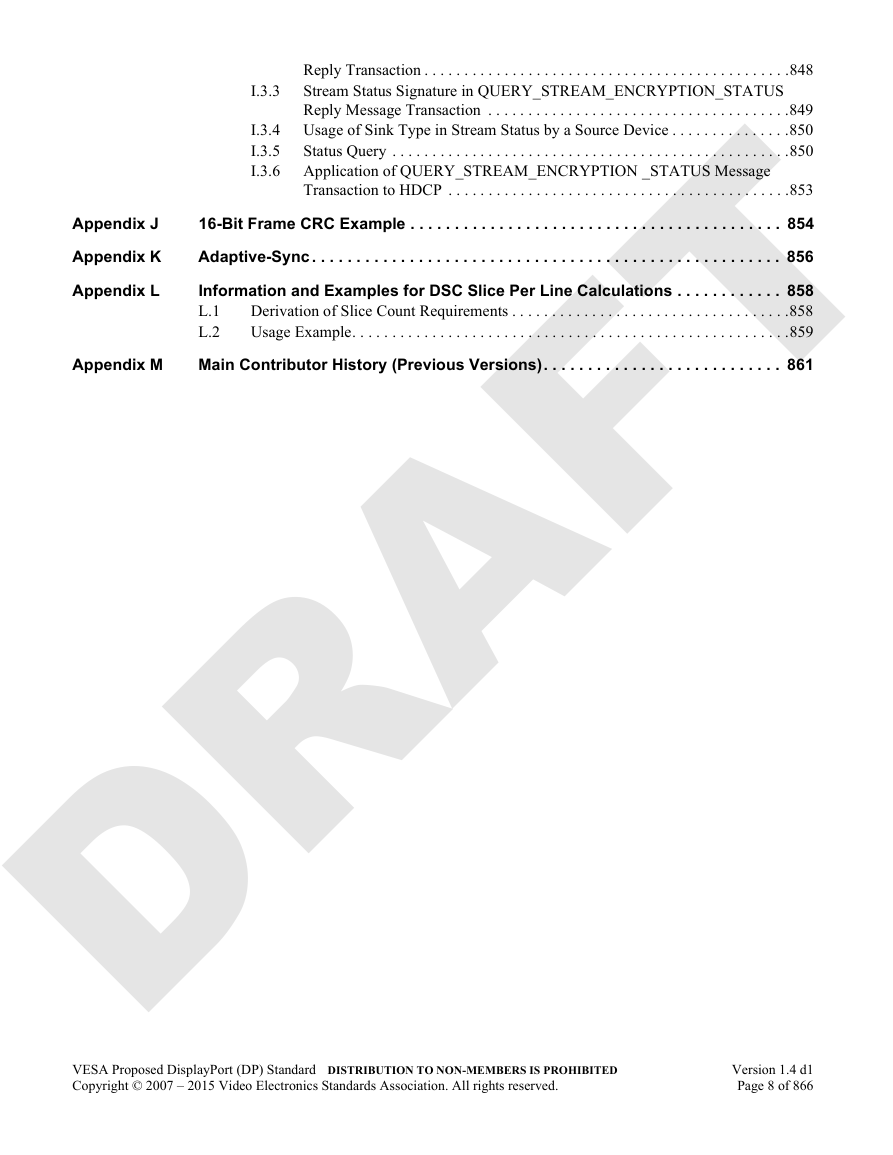
I.3.2 Stream Status in QUERY_STREAM_ENCRYPTION_STATUS Reply Transaction
I.3.3 Stream Status Signature in QUERY_STREAM_ENCRYPTION_STATUS Reply Message Transaction
I.3.4 Usage of Sink Type in Stream Status by a Source Device
I.3.5 Status Query
I.3.6 Application of QUERY_STREAM_ENCRYPTION _STATUS Message Transaction to HDCP
J 16-Bit Frame CRC Example
K Adaptive-Sync
L Information and Examples for DSC Slice Per Line Calculations
L.1 Derivation of Slice Count Requirements
L.2 Usage Example
M Main Contributor History (Previous Versions)


 2023年江西萍乡中考道德与法治真题及答案.doc
 2012年重庆南川中考生物真题及答案.doc
 2013年江西师范大学地理学综合及文艺理论基础考研真题.doc
 2020年四川甘孜小升初语文真题及答案I卷.doc
 2020年注册岩土工程师专业基础考试真题及答案.doc
 2023-2024学年福建省厦门市九年级上学期数学月考试题及答案.doc
 2021-2022学年辽宁省沈阳市大东区九年级上学期语文期末试题及答案.doc
 2022-2023学年北京东城区初三第一学期物理期末试卷及答案.doc
 2018上半年江西教师资格初中地理学科知识与教学能力真题及答案.doc
 2012年河北国家公务员申论考试真题及答案-省级.doc
 2020-2021学年江苏省扬州市江都区邵樊片九年级上学期数学第一次质量检测试题及答案.doc
 2022下半年黑龙江教师资格证中学综合素质真题及答案.doc