Freescale Semiconductor
MPC5604BCRM
Rev. 8.1, 05/2012
MPC5604B/C Microcontroller
Reference Manual
by: Microcontroller Solutions Group
This is the MPC5604B/C Reference Manual set consisting of the following files:
• MPC5604B/C Reference Manual Addendum (MPC5604B/CRMAD), Rev. 1
• MPC5604B/C Reference Manual (MPC5604B/CRM), Rev. 8
© Freescale Semiconductor, Inc., 2012. All rights reserved.
�
Freescale Semiconductor
Reference Manual Addendum
MPC5604BRMAD
Rev. 1, 05/2012
MPC5604B/C Microcontroller
Reference Manual Addendum
by: Microcontroller Solutions Group
This addendum document describes corrections to the
MPC5604B/C Microcontroller Reference Manual, order
number MPC5604BCRM. For convenience, the addenda
items are grouped by revision. Please check our website
at http://www.freescale.com/powerarchitecture for the
latest updates.
The current version available of the MPC5604B/C
Microcontroller Reference Manual is Revision 8.
Table of Contents
1
2
Addendum for Revision 8 . . . . . . . . . . . . . . . . . . . 2
Revision History . . . . . . . . . . . . . . . . . . . . . . . . . . 4
© Freescale Semiconductor, Inc., 2012. All rights reserved.
�
Addendum List for Revision 8
1
Addendum List for Revision 8
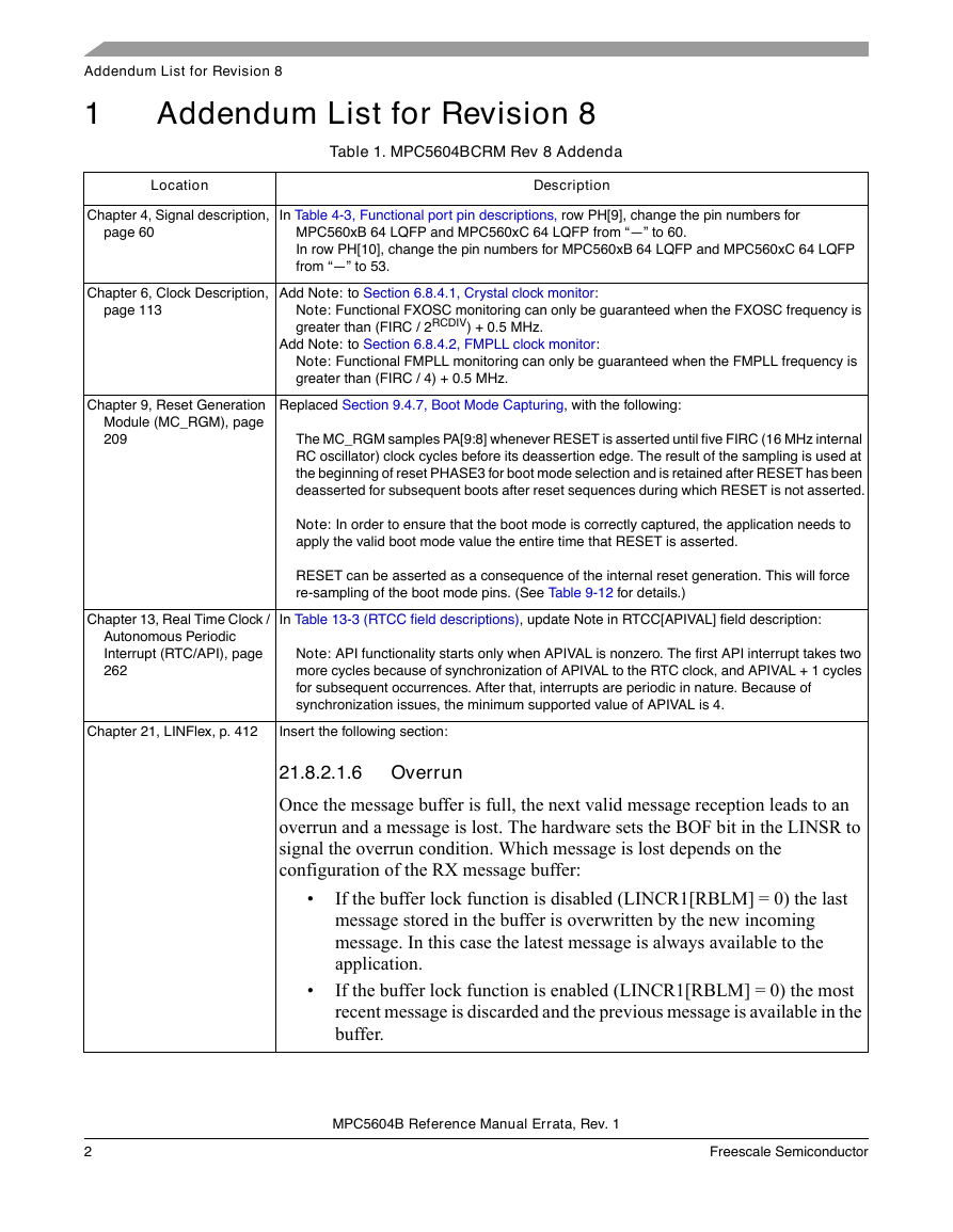
Table 1. MPC5604BCRM Rev 8 Addenda
Location
Description
Chapter 4, Signal description,
In Table 4-3, Functional port pin descriptions, row PH[9], change the pin numbers for
page 60
MPC560xB 64 LQFP and MPC560xC 64 LQFP from “—” to 60.
In row PH[10], change the pin numbers for MPC560xB 64 LQFP and MPC560xC 64 LQFP
from “—” to 53.
Chapter 6, Clock Description,
Add Note: to Section 6.8.4.1, Crystal clock monitor:
page 113
Chapter 9, Reset Generation
Module (MC_RGM), page
209
Note: Functional FXOSC monitoring can only be guaranteed when the FXOSC frequency is
greater than (FIRC / 2RCDIV) + 0.5 MHz.
Add Note: to Section 6.8.4.2, FMPLL clock monitor:
Note: Functional FMPLL monitoring can only be guaranteed when the FMPLL frequency is
greater than (FIRC / 4) + 0.5 MHz.
Replaced Section 9.4.7, Boot Mode Capturing, with the following:
The MC_RGM samples PA[9:8] whenever RESET is asserted until five FIRC (16 MHz internal
RC oscillator) clock cycles before its deassertion edge. The result of the sampling is used at
the beginning of reset PHASE3 for boot mode selection and is retained after RESET has been
deasserted for subsequent boots after reset sequences during which RESET is not asserted.
Note: In order to ensure that the boot mode is correctly captured, the application needs to
apply the valid boot mode value the entire time that RESET is asserted.
RESET can be asserted as a consequence of the internal reset generation. This will force
re-sampling of the boot mode pins. (See Table 9-12 for details.)
Chapter 13, Real Time Clock /
In Table 13-3 (RTCC field descriptions), update Note in RTCC[APIVAL] field description:
Autonomous Periodic
Interrupt (RTC/API), page
262
Note: API functionality starts only when APIVAL is nonzero. The first API interrupt takes two
more cycles because of synchronization of APIVAL to the RTC clock, and APIVAL + 1 cycles
for subsequent occurrences. After that, interrupts are periodic in nature. Because of
synchronization issues, the minimum supported value of APIVAL is 4.
Chapter 21, LINFlex, p. 412
Insert the following section:
21.8.2.1.6 Overrun
Once the message buffer is full, the next valid message reception leads to an
overrun and a message is lost. The hardware sets the BOF bit in the LINSR to
signal the overrun condition. Which message is lost depends on the
configuration of the RX message buffer:
•
•
If the buffer lock function is disabled (LINCR1[RBLM] = 0) the last
message stored in the buffer is overwritten by the new incoming
message. In this case the latest message is always available to the
application.
If the buffer lock function is enabled (LINCR1[RBLM] = 0) the most
recent message is discarded and the previous message is available in the
buffer.
2
Freescale Semiconductor
MPC5604B Reference Manual Errata, Rev. 1
�
Addendum List for Revision 8
Location
Chapter 22, FlexCAN,
throughout chapter
Table 1. MPC5604BCRM Rev 8 Addenda
Description
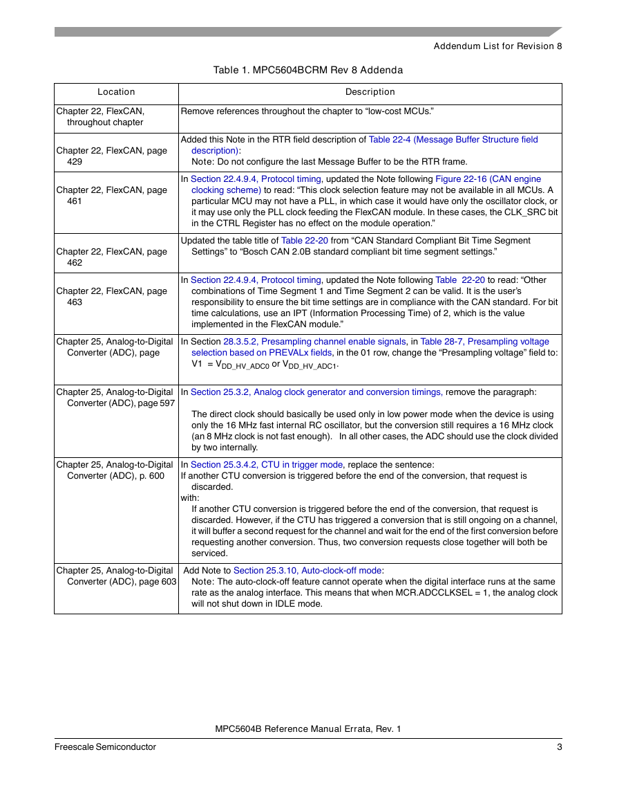
Remove references throughout the chapter to “low-cost MCUs.”
Chapter 22, FlexCAN, page
429
description):
Note: Do not configure the last Message Buffer to be the RTR frame.
Added this Note in the RTR field description of Table 22-4 (Message Buffer Structure field
Chapter 22, FlexCAN, page
461
In Section 22.4.9.4, Protocol timing, updated the Note following Figure 22-16 (CAN engine
clocking scheme) to read: “This clock selection feature may not be available in all MCUs. A
particular MCU may not have a PLL, in which case it would have only the oscillator clock, or
it may use only the PLL clock feeding the FlexCAN module. In these cases, the CLK_SRC bit
in the CTRL Register has no effect on the module operation.”
Chapter 22, FlexCAN, page
Settings” to “Bosch CAN 2.0B standard compliant bit time segment settings.”
Updated the table title of Table 22-20 from “CAN Standard Compliant Bit Time Segment
462
Chapter 22, FlexCAN, page
463
In Section 22.4.9.4, Protocol timing, updated the Note following Table 22-20 to read: “Other
combinations of Time Segment 1 and Time Segment 2 can be valid. It is the user’s
responsibility to ensure the bit time settings are in compliance with the CAN standard. For bit
time calculations, use an IPT (Information Processing Time) of 2, which is the value
implemented in the FlexCAN module.”
Chapter 25, Analog-to-Digital
In Section 28.3.5.2, Presampling channel enable signals, in Table 28-7, Presampling voltage
Converter (ADC), page
selection based on PREVALx fields, in the 01 row, change the “Presampling voltage” field to:
V1 = VDD_HV_ADC0 or VDD_HV_ADC1.
Chapter 25, Analog-to-Digital
Converter (ADC), page 597
In Section 25.3.2, Analog clock generator and conversion timings, remove the paragraph:
The direct clock should basically be used only in low power mode when the device is using
only the 16 MHz fast internal RC oscillator, but the conversion still requires a 16 MHz clock
(an 8 MHz clock is not fast enough). In all other cases, the ADC should use the clock divided
by two internally.
Chapter 25, Analog-to-Digital
Converter (ADC), p. 600
In Section 25.3.4.2, CTU in trigger mode, replace the sentence:
If another CTU conversion is triggered before the end of the conversion, that request is
discarded.
with:
If another CTU conversion is triggered before the end of the conversion, that request is
discarded. However, if the CTU has triggered a conversion that is still ongoing on a channel,
it will buffer a second request for the channel and wait for the end of the first conversion before
requesting another conversion. Thus, two conversion requests close together will both be
serviced.
Chapter 25, Analog-to-Digital
Converter (ADC), page 603
Add Note to Section 25.3.10, Auto-clock-off mode:
Note: The auto-clock-off feature cannot operate when the digital interface runs at the same
rate as the analog interface. This means that when MCR.ADCCLKSEL = 1, the analog clock
will not shut down in IDLE mode.
Freescale Semiconductor
3
MPC5604B Reference Manual Errata, Rev. 1
�
Revision History
Location
Chapter 25, Analog-to-Digital
Converter (ADC), page 610
Table 1. MPC5604BCRM Rev 8 Addenda
Description
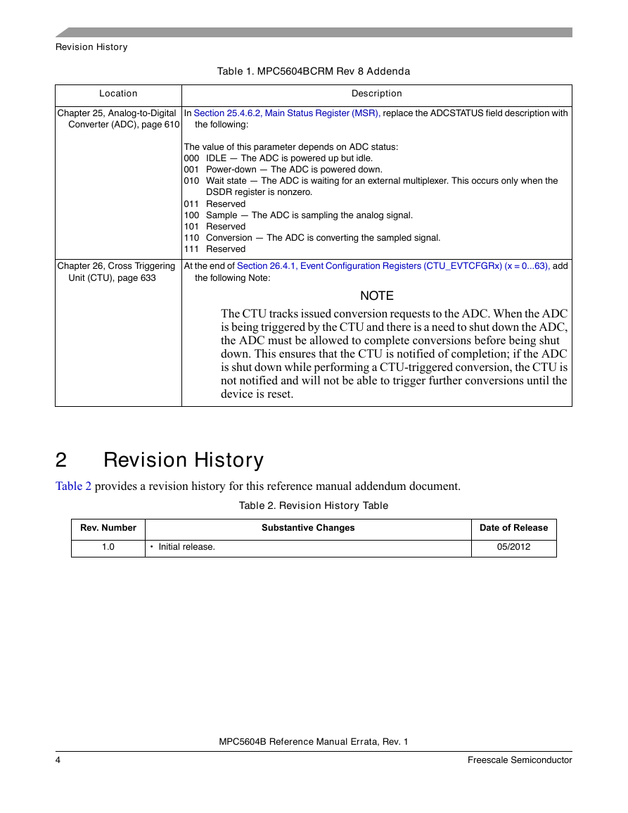
In Section 25.4.6.2, Main Status Register (MSR), replace the ADCSTATUS field description with
the following:
The value of this parameter depends on ADC status:
000 IDLE — The ADC is powered up but idle.
001 Power-down — The ADC is powered down.
010 Wait state — The ADC is waiting for an external multiplexer. This occurs only when the
DSDR register is nonzero.
011 Reserved
100 Sample — The ADC is sampling the analog signal.
101 Reserved
110 Conversion — The ADC is converting the sampled signal.
111 Reserved
Chapter 26, Cross Triggering
At the end of Section 26.4.1, Event Configuration Registers (CTU_EVTCFGRx) (x = 0...63), add
Unit (CTU), page 633
the following Note:
NOTE
The CTU tracks issued conversion requests to the ADC. When the ADC
is being triggered by the CTU and there is a need to shut down the ADC,
the ADC must be allowed to complete conversions before being shut
down. This ensures that the CTU is notified of completion; if the ADC
is shut down while performing a CTU-triggered conversion, the CTU is
not notified and will not be able to trigger further conversions until the
device is reset.
Revision History
2
Table 2 provides a revision history for this reference manual addendum document.
Table 2. Revision History Table
Rev. Number
Substantive Changes
1.0
Initial release.
Date of Release
05/2012
4
Freescale Semiconductor
MPC5604B Reference Manual Errata, Rev. 1
�
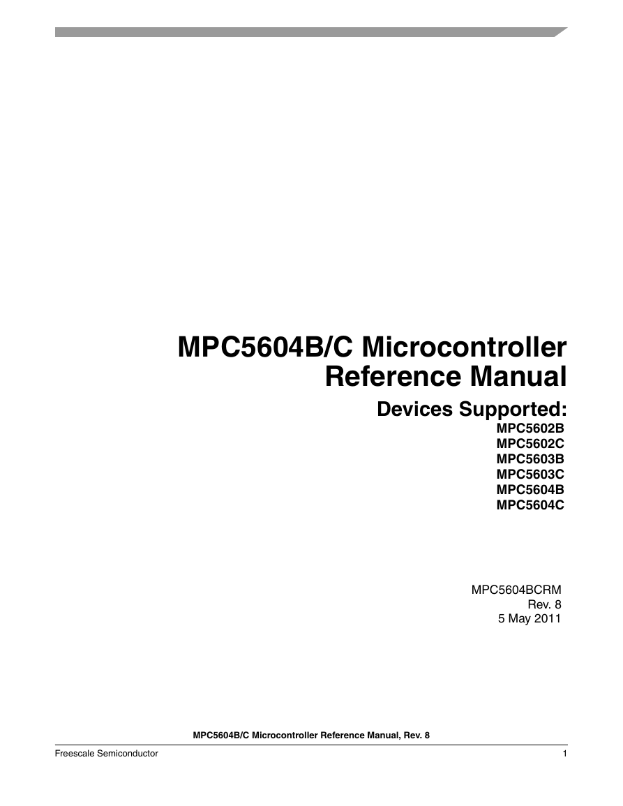
MPC5604B/C Microcontroller
Reference Manual
Devices Supported:
MPC5602B
MPC5602C
MPC5603B
MPC5603C
MPC5604B
MPC5604C
MPC5604BCRM
Rev. 8
5 May 2011
MPC5604B/C Microcontroller Reference Manual, Rev. 8
Freescale Semiconductor
1
�
MPC5604B/C Microcontroller Reference Manual, Rev. 8
2
Freescale Semiconductor
�
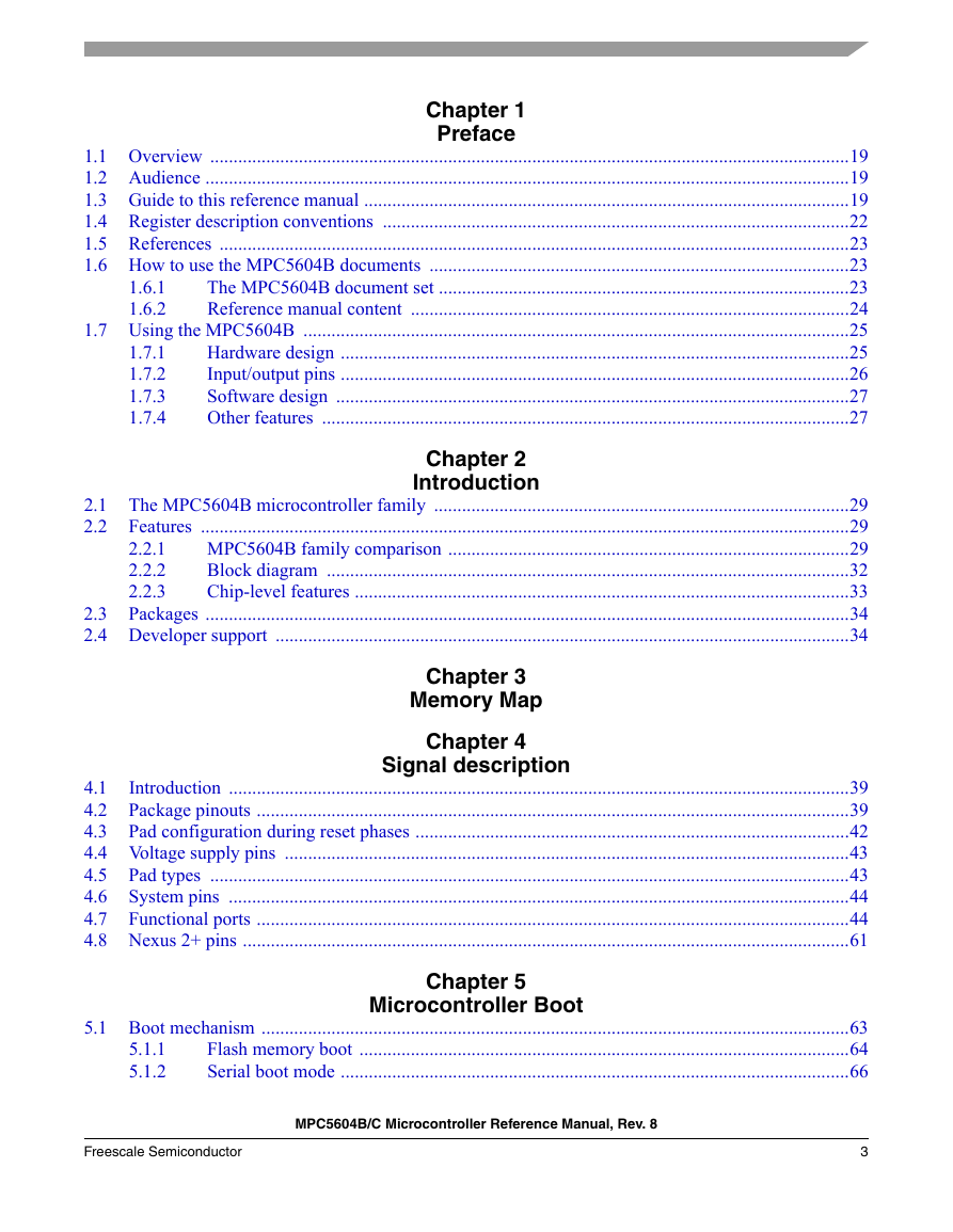
Chapter 1
Preface
1.1 Overview .........................................................................................................................................19
1.2 Audience ..........................................................................................................................................19
1.3 Guide to this reference manual ........................................................................................................19
1.4 Register description conventions ....................................................................................................22
1.5 References .......................................................................................................................................23
1.6 How to use the MPC5604B documents ..........................................................................................23
The MPC5604B document set ........................................................................................23
Reference manual content ..............................................................................................24
1.7 Using the MPC5604B .....................................................................................................................25
Hardware design .............................................................................................................25
Input/output pins .............................................................................................................26
Software design ..............................................................................................................27
Other features .................................................................................................................27
1.7.1
1.7.2
1.7.3
1.7.4
1.6.1
1.6.2
Chapter 2
Introduction
2.1 The MPC5604B microcontroller family .........................................................................................29
Features ...........................................................................................................................................29
2.2
MPC5604B family comparison ......................................................................................29
2.2.1
2.2.2
Block diagram ................................................................................................................32
2.2.3
Chip-level features ..........................................................................................................33
2.3
Packages ..........................................................................................................................................34
2.4 Developer support ...........................................................................................................................34
Chapter 3
Memory Map
Chapter 4
Signal description
4.1
Introduction .....................................................................................................................................39
4.2
Package pinouts ...............................................................................................................................39
4.3
Pad configuration during reset phases .............................................................................................42
4.4 Voltage supply pins .........................................................................................................................43
Pad types .........................................................................................................................................43
4.5
4.6
System pins .....................................................................................................................................44
4.7
Functional ports ...............................................................................................................................44
4.8 Nexus 2+ pins ..................................................................................................................................61
Chapter 5
Microcontroller Boot
5.1 Boot mechanism ..............................................................................................................................63
Flash memory boot .........................................................................................................64
Serial boot mode .............................................................................................................66
5.1.1
5.1.2
MPC5604B/C Microcontroller Reference Manual, Rev. 8
Freescale Semiconductor
3
�



 2023年江西萍乡中考道德与法治真题及答案.doc
 2012年重庆南川中考生物真题及答案.doc
 2013年江西师范大学地理学综合及文艺理论基础考研真题.doc
 2020年四川甘孜小升初语文真题及答案I卷.doc
 2020年注册岩土工程师专业基础考试真题及答案.doc
 2023-2024学年福建省厦门市九年级上学期数学月考试题及答案.doc
 2021-2022学年辽宁省沈阳市大东区九年级上学期语文期末试题及答案.doc
 2022-2023学年北京东城区初三第一学期物理期末试卷及答案.doc
 2018上半年江西教师资格初中地理学科知识与教学能力真题及答案.doc
 2012年河北国家公务员申论考试真题及答案-省级.doc
 2020-2021学年江苏省扬州市江都区邵樊片九年级上学期数学第一次质量检测试题及答案.doc
 2022下半年黑龙江教师资格证中学综合素质真题及答案.doc