Signal and Power Isolated RS-485
Transceiver with ±15 kV ESD Protection
ADM2582E/ADM2587E
FEATURES
Isolated RS-485/RS-422 transceiver, configurable as half or
full duplex
isoPower® integrated isolated dc-to-dc converter
±15 kV ESD protection on RS-485 input/output pins
Complies with ANSI/TIA/EIA-485-A-98 and ISO 8482:1987(E)
ADM2582E data rate: 16 Mbps
ADM2587E data rate: 500 kbps
5 V or 3.3 V operation
Connect up to 256 nodes on one bus
Open- and short-circuit, fail-safe receiver inputs
High common-mode transient immunity: >25 kV/μs
Thermal shutdown protection
Safety and regulatory approvals (pending)
UL recognition: 2500 V rms for 1 minute per UL 1577
VDE Certificates of Conformity
DIN V VDE V 0884-10 (VDE V 0884-10):2006-12
VIORM = 560 V peak
Operating temperature range: −40°C to +85°C
Highly integrated, 20-lead, wide-body SOIC package
APPLICATIONS
Isolated RS-485/RS-422 interfaces
Industrial field networks
Multipoint data transmission systems
GENERAL DESCRIPTION
The ADM2582E/ADM2587E are fully integrated signal and
power isolated data transceivers with ±15 kV ESD protection
and are suitable for high speed communication on multipoint
transmission lines. The ADM2582E/ADM2587E include an
integrated isolated dc-to-dc power supply, which eliminates the
need for an external dc-to-dc isolation block.
They are designed for balanced transmission lines and comply
with ANSI/TIA/EIA-485-A-98 and ISO 8482:1987(E).
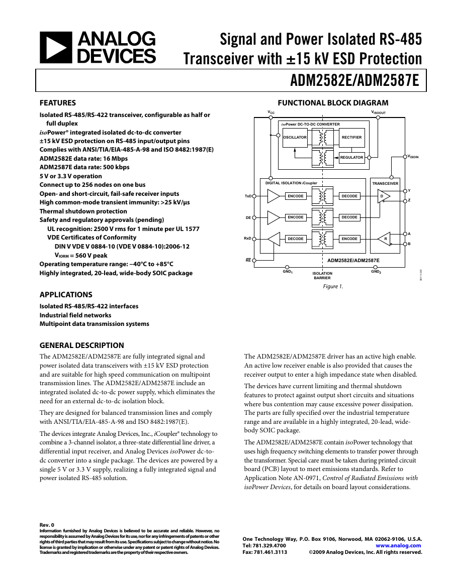
The devices integrate Analog Devices, Inc., iCoupler® technology to
combine a 3-channel isolator, a three-state differential line driver, a
differential input receiver, and Analog Devices isoPower dc-to-
dc converter into a single package. The devices are powered by a
single 5 V or 3.3 V supply, realizing a fully integrated signal and
power isolated RS-485 solution.
FUNCTIONAL BLOCK DIAGRAM
VISOOUT
VCC
isoPower DC-TO-DC CONVERTER
OSCILLATOR
RECTIFIER
REGULATOR
VISOIN
TxD
DE
RxD
RE
DIGITAL ISOLATION iCoupler
TRANSCEIVER
ENCODE
DECODE
D
ENCODE
DECODE
DECODE
ENCODE
R
Y
Z
A
B
ADM2582E/ADM2587E
GND1
ISOLATION
BARRIER
Figure 1.
GND2
1
0
0
-
1
1
1
8
0
The ADM2582E/ADM2587E driver has an active high enable.
An active low receiver enable is also provided that causes the
receiver output to enter a high impedance state when disabled.
The devices have current limiting and thermal shutdown
features to protect against output short circuits and situations
where bus contention may cause excessive power dissipation.
The parts are fully specified over the industrial temperature
range and are available in a highly integrated, 20-lead, wide-
body SOIC package.
The ADM2582E/ADM2587E contain isoPower technology that
uses high frequency switching elements to transfer power through
the transformer. Special care must be taken during printed circuit
board (PCB) layout to meet emissions standards. Refer to
Application Note AN-0971, Control of Radiated Emissions with
isoPower Devices, for details on board layout considerations.
Rev. 0
Information furnished by Analog Devices is believed to be accurate and reliable. However, no
responsibility is assumed by Analog Devices for its use, nor for any infringements of patents or other
rights of third parties that may result from its use. Specifications subject to change without notice. No
license is granted by implication or otherwise under any patent or patent rights of Analog Devices.
Trademarks and registered trademarks are the property of their respective owners.
One Technology Way, P.O. Box 9106, Norwood, MA 02062-9106, U.S.A.
www.analog.com
Tel: 781.329.4700
©2009 Analog Devices, Inc. All rights reserved.
Fax: 781.461.3113
�
ADM2582E/ADM2587E
TABLE OF CONTENTS
Features .............................................................................................. 1
Applications ....................................................................................... 1
Functional Block Diagram .............................................................. 1
General Description ......................................................................... 1
Revision History ............................................................................... 2
Specifications ..................................................................................... 3
ADM2582E Timing Specifications ............................................ 4
ADM2587E Timing Specifications ............................................ 4
ADM2582E/ADM2587E Package Characteristics ................... 4
ADM2582E/ADM2587E Regulatory Information .................. 5
ADM2582E/ADM2587E Insulation and Safety-Related
Specifications ................................................................................ 5
ADM2582E/ADM2587E VDE 0884 Insulation
Characteristics (Pending) ............................................................ 5
Absolute Maximum Ratings ............................................................ 6
ESD Caution .................................................................................. 6
Pin Configuration and Function Descriptions ............................. 7
Typical Performance Characteristics ............................................. 8
REVISION HISTORY
9/09—Revision 0: Initial Version
Test Circuits ..................................................................................... 12
Switching Characteristics .............................................................. 13
Circuit Description......................................................................... 14
Signal Isolation ........................................................................... 14
Power Isolation ........................................................................... 14
Truth Tables................................................................................. 14
Thermal Shutdown .................................................................... 14
Open- and Short-Circuit, Fail-Safe Receiver Inputs.............. 14
DC Correctness and Magnetic Field Immunity ........................... 15
Applications Information .............................................................. 16
PCB Layout ................................................................................. 16
EMI Considerations ................................................................... 16
Insulation Lifetime ..................................................................... 16
Isolated Power Supply Considerations .................................... 17
Typical Applications ................................................................... 19
Outline Dimensions ....................................................................... 20
Ordering Guide .......................................................................... 20
Rev. 0 | Page 2 of 20
�
ADM2582E/ADM2587E
SPECIFICATIONS
All voltages are relative to their respective ground; 3.0 ≤ VCC ≤ 5.5 V. All minimum/maximum specifications apply over the entire
recommended operation range, unless otherwise noted. All typical specifications are at TA = 25°C, VCC = 5 V unless otherwise noted.
Table 1.
Parameter
ADM2587E SUPPLY CURRENT
Data Rate ≤ 500 kbps
ADM2582E SUPPLY CURRENT
Data Rate = 16 Mbps
ISOLATED SUPPLY VOLTAGE
DRIVER
Differential Outputs
Differential Output Voltage, Loaded
Δ|VOD| for Complementary Output States
Common-Mode Output Voltage
Δ|VOC| for Complementary Output States
Short-Circuit Output Current
Output Leakage Current (Y, Z)
Symbol Min
ICC
ICC
VISOUT
|VOD2|
|VOD3|
Δ|VOD|
VOC
Δ|VOC|
IOS
IO
2.0
1.5
1.5
Typ
90
72
125
98
3.3
Max
120
150
230
5.0
5.0
5.0
0.2
3.0
0.2
200
30
−30
Logic Inputs DE, RE, TxD
Input Threshold Low
Input Threshold High
Input Current
RECEIVER
Differential Inputs
Differential Input Threshold Voltage
Input Voltage Hysteresis
Input Current (A, B)
Line Input Resistance
Logic Outputs
Output Voltage Low
Output Voltage High
Short-Circuit Current
VIL
VIH
II
VTH
VHYS
II
RIN
VOL
VOH V
0.3 × VCC
−10
−200
−100
96
0.01
−125
15
0.2
CC − 0.3 VCC − 0.2
V
0.7 × VCC V
10
−30
125
0.4
100
Unit
mA
mA
mA
mA
mA
mA
mA
V
V
V
V
V
V
mA
μA
μA
Test Conditions
VCC = 3.3 V, 100 Ω load between Y and Z
VCC = 5 V, 100 Ω load between Y and Z
VCC = 3.3 V, 54 Ω load between Y and Z
VCC = 5 V, 54 Ω load between Y and Z
120 Ω load between Y and Z
120 Ω load between Y and Z
54 Ω load between Y and Z
RL = 100 Ω (RS-422), see Figure 23
RL = 54 Ω (RS-485), see Figure 23
−7 V ≤ VTEST1 ≤ 12 V, see Figure 24
RL = 54 Ω or 100 Ω, see Figure 23
RL = 54 Ω or 100 Ω, see Figure 23
RL = 54 Ω or 100 Ω, see Figure 23
DE = 0 V, RE = 0 V, VCC = 0 V or 3.6 V,
VIN = 12 V
DE = 0 V, RE = 0 V, VCC = 0 V or 3.6 V,
VIN = −7 V
DE, RE, TxD
DE, RE, TxD
DE, RE, TxD
−7 V < VCM < +12 V
VOC = 0 V
DE = 0 V, VCC = 0 V or 3.6 V, VIN = 12 V
DE = 0 V, VCC = 0 V or 3.6 V, VIN = -7 V
−7 V < VCM < +12 V
IO = 1.5 mA, VA − VB = −0.2 V
IO = −1.5 mA, VA − VB = 0.2 V
μA
mV
mV
μA
μA
kΩ
V
V
mA
kV/μs VCM = 1 kV, transient magnitude = 800 V
COMMON-MODE TRANSIENT IMMUNITY1
1 CM is the maximum common-mode voltage slew rate that can be sustained while maintaining specification-compliant operation. VCM is the common-mode potential
difference between the logic and bus sides. The transient magnitude is the range over which the common-mode is slewed. The common-mode voltage slew rates
apply to both rising and falling common-mode voltage edges.
25
Rev. 0 | Page 3 of 20
�
ADM2582E/ADM2587E
ADM2582E TIMING SPECIFICATIONS
TA = −40°C to +85°C.
Table 2.
Parameter
DRIVER
Maximum Data Rate
Propagation Delay, Low to High
Propagation Delay, High to Low
Output Skew
Rise Time/Fall Time
Enable Time
Disable Time
RECEIVER
Propagation Delay, Low to High
Propagation Delay, High to Low
Output Skew1 t
Enable Time
Disable Time
1 Guaranteed by design.
Symbol Min
tDPLH
tDPHL
tSKEW
tDR, tDF
tZL, tZH
tLZ, tHZ
tRPLH
tRPHL
SKEW
tZL, tZH
tLZ, tHZ
16
ADM2587E TIMING SPECIFICATIONS
TA = −40°C to +85°C.
Test Conditions
RL = 54 Ω, CL1 = C L2 = 100 pF, see Figure 25 and Figure 29
RL = 54 Ω, CL1 = C L2 = 100 pF, see Figure 25 and Figure 29
RL = 54 Ω, CL1 = CL2 = 100 pF, see Figure 25 and Figure 29
RL = 54 Ω, CL1 = CL2 = 100 pF, see Figure 25 and Figure 29
RL = 110 Ω, CL = 50 pF, see Figure 26 and Figure 31
RL = 110 Ω, CL = 50 pF, see Figure 26 and Figure 31
CL = 15 pF, see Figure 27 and Figure 30
CL = 15 pF, see Figure 27 and Figure 30
CL = 15 pF, see Figure 27 and Figure 30
RL = 1 kΩ, CL = 15 pF, see Figure 28 and Figure 32
RL = 1 kΩ, CL = 15 pF, see Figure 28 and Figure 32
Typ Max Unit
63
64
1
94
95
1
Mbps
ns
ns
ns
ns
ns
ns
ns
ns
ns
ns
ns
100
100
8
15
120
150
110
110
12
15
15
Table 3.
Parameter
DRIVER
Maximum Data Rate
Propagation Delay, Low to High
Propagation Delay, High to Low
Output Skew
Rise Time/Fall Time
Enable Time
Disable Time
RECEIVER
Propagation Delay, Low to High
Propagation Delay, High to Low
Output Skew
Enable Time
Disable Time
Symbol Min
tDPLH
tDPHL
tSKEW
tDR, tDF
tZL, tZH
tLZ, tHZ
tRPLH
tRPHL
tSKEW
tZL, tZH
tLZ, tHZ
500
250
250
200
Typ Max
503
510
7
91
95
4
700
700
100
1100
2.5
200
200
200
30
15
15
Unit
kbps
ns
ns
ns
ns
μs
ns
ns
ns
ns
ns
ns
Test Conditions
RL = 54 Ω, CL1 = C L2 = 100 pF, see Figure 25 and Figure 29
RL = 54 Ω, CL1 = C L2 = 100 pF, see Figure 25 and Figure 29
RL = 54 Ω, CL1 = CL2 = 100 pF, see Figure 25 and Figure 29
RL = 54 Ω, CL1 = CL2 = 100 pF, see Figure 25 and Figure 29
RL = 110 Ω, CL = 50 pF, see Figure 26 and Figure 31
RL = 110 Ω, CL = 50 pF, see Figure 26 and Figure 31
CL = 15 pF, see Figure 27 and Figure 30
CL = 15 pF, see Figure 27 and Figure 30
CL = 15 pF, see Figure 27 and Figure 30
RL = 1 kΩ, CL = 15 pF, see Figure 28 and Figure 32
RL = 1 kΩ, CL = 15 pF, see Figure 28 and Figure 32
ADM2582E/ADM2587E PACKAGE CHARACTERISTICS
Table 4.
Parameter
Resistance (Input-to-Output)1 R
Capacitance (Input-to-Output)1 C
Input Capacitance2 C
Input IC Junction-to-Case Thermal Resistance
Symbol Min
I-O
I-O
I
θJCI
Typ Max
1012
3
4
33
Output IC Junction-to-Case Thermal Resistance
θJCO
28
1 Device considered a 2-terminal device: short together Pin 1 to Pin 10 and short together Pin 11 to Pin 20.
2 Input capacitance is from any input data pin to ground.
Rev. 0 | Page 4 of 20
Unit
Ω
pF
pF
°C/W
°C/W
Test Conditions
f = 1 MHz
Thermocouple located at center of
package underside
Thermocouple located at center of
package underside
�
ADM2582E/ADM2587E REGULATORY INFORMATION
ADM2582E/ADM2587E
Table 5. Pending ADM2582E/ADM2587E Approvals
Organization Approval Type
UL
To be recognized under the Component
Recognition Program of Underwriters
Laboratories, Inc.
To be certified according to
DIN V VDE V 0884-10 (VDE V 0884-10):2006-12
VDE
Notes
In accordance with UL 1577, each ADM2582E/ADM2587E is proof tested
by applying an insulation test voltage ≥ 3000 V rms for 1 second.
In accordance with VDE 0884-10, each ADM2582E/ADM2587E is proof
tested by applying an insulation test voltage ≥ 1050 VPEAK for 1 second.
ADM2582E/ADM2587E INSULATION AND SAFETY-RELATED SPECIFICATIONS
Table 6.
Parameter
Rated Dielectric Insulation Voltage
Minimum External Air Gap (Clearance)
Symbol Value
2500
L(I01)
>8.0
Unit
V rms
mm
Minimum External Tracking (Creepage)
L(I02)
>8.0
mm
Conditions
1-minute duration
Measured from input terminals to output terminals,
shortest distance through air
Measured from input terminals to output terminals,
shortest distance along body
Insulation distance through insulation
DIN IEC 112/VDE 0303-1
Material Group (DIN VDE 0110: 1989-01, Table 1)
Minimum Internal Gap (Internal Clearance)
Tracking Resistance (Comparative Tracking Index)
Isolation Group
ADM2582E/ADM2587E VDE 0884 INSULATION CHARACTERISTICS (PENDING)
This isolator is suitable for basic electrical isolation only within the safety limit data. Maintenance of the safety data must be ensured by
means of protective circuits.
0.017 min mm
>175
IIIa
CTI
V
Table 7.
Description
CLASSIFICATIONS
Installation Classification per DIN VDE 0110 for
Conditions
Symbol Characteristic Unit
Rated Mains Voltage
≤150 V rms
≤300 V rms
≤400 V rms
Climatic Classification
Pollution Degree
VOLTAGE
Maximum Working Insulation Voltage
Input-to-Output Test Voltage
Method b1
Method a
After Environmental Tests, Subgroup 1
After Input and/or Safety Test,
Subgroup 2/Subgroup 3
Highest Allowable Overvoltage
SAFETY-LIMITING VALUES
Case Temperature
Input Current
Output Current
Insulation Resistance at TS V
DIN VDE 0110, see Table 1
VIORM × 1.875 = VPR, 100% production tested,
tm = 1 sec, partial discharge < 5 pC
VIORM × 1.6 = VPR, tm = 60 sec, partial discharge < 5 pC
VIORM × 1.2 = VPR, tm = 60 sec, partial discharge < 5 pC
VIORM
VPR
Transient overvoltage, tTR = 10 sec
Maximum value allowed in the event of a failure
IO = 500 V
VTR
TS
IS, INPUT
IS, OUTPUT
RS
I to IV
I to III
I to II
40/85/21
2
560
1050
896
672
4000
150
265
335
>109
V peak
V peak
V peak
V peak
V peak
°C
mA
mA
Ω
Rev. 0 | Page 5 of 20
�
ADM2582E/ADM2587E
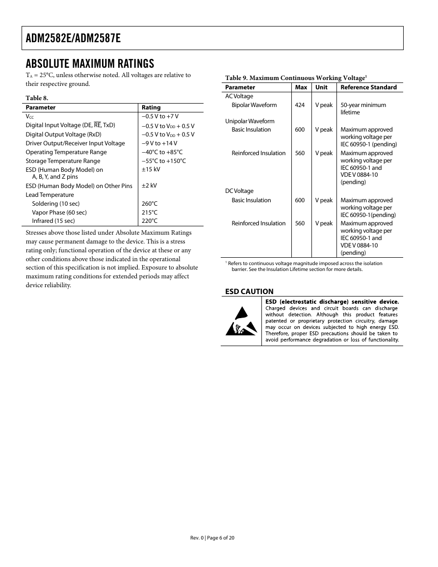
ABSOLUTE MAXIMUM RATINGS
TA = 25°C, unless otherwise noted. All voltages are relative to
their respective ground.
Table 8.
Parameter
VCC
Digital Input Voltage (DE, RE, TxD)
Digital Output Voltage (RxD)
Driver Output/Receiver Input Voltage
Operating Temperature Range
Storage Temperature Range
ESD (Human Body Model) on
A, B, Y, and Z pins
ESD (Human Body Model) on Other Pins
Lead Temperature
Soldering (10 sec)
Vapor Phase (60 sec)
Infrared (15 sec)
Rating
−0.5 V to +7 V
−0.5 V to VDD + 0.5 V
−0.5 V to VDD + 0.5 V
−9 V to +14 V
−40°C to +85°C
−55°C to +150°C
±15 kV
±2 kV
260°C
215°C
220°C
Stresses above those listed under Absolute Maximum Ratings
may cause permanent damage to the device. This is a stress
rating only; functional operation of the device at these or any
other conditions above those indicated in the operational
section of this specification is not implied. Exposure to absolute
maximum rating conditions for extended periods may affect
device reliability.
Table 9. Maximum Continuous Working Voltage1
Parameter
AC Voltage
Max Unit
424
V peak
Bipolar Waveform
Unipolar Waveform
Basic Insulation
600
Reinforced Insulation
560
DC Voltage
Basic Insulation
600
Reinforced Insulation
560
Reference Standard
50-year minimum
lifetime
V peak Maximum approved
working voltage per
IEC 60950-1 (pending)
V peak Maximum approved
working voltage per
IEC 60950-1 and
VDE V 0884-10
(pending)
V peak Maximum approved
working voltage per
IEC 60950-1(pending)
V peak Maximum approved
working voltage per
IEC 60950-1 and
VDE V 0884-10
(pending)
1 Refers to continuous voltage magnitude imposed across the isolation
barrier. See the Insulation Lifetime section for more details.
ESD CAUTION
Rev. 0 | Page 6 of 20
�
ADM2582E/ADM2587E
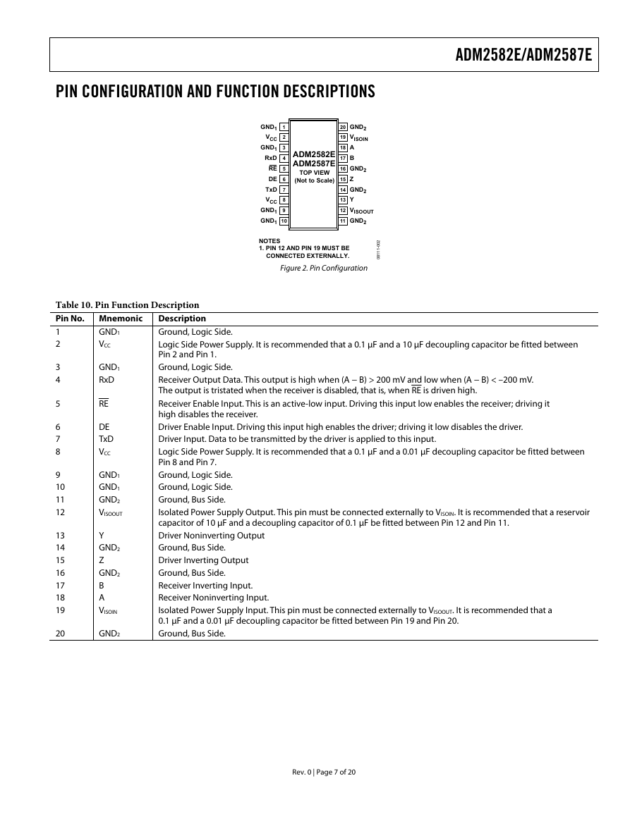
PIN CONFIGURATION AND FUNCTION DESCRIPTIONS
GND2
VISOIN
GND2
GND2
ADM2582E
ADM2587E
TOP VIEW
(Not to Scale)
GND1 1
VCC 2
GND1 3
RxD 4
RE 5
DE 6
TxD 7
VCC 8
GND1 9
GND1 10
20
19
A18
B17
16
Z15
14
Y13
12
11
VISOOUT
GND2
NOTES
1. PIN 12 AND PIN 19 MUST BE
CONNECTED EXTERNALLY.
2
0
0
-
1
1
1
8
0
Figure 2. Pin Configuration
Table 10. Pin Function Description
Pin No. Mnemonic
1
2
GND1
VCC
Description
Ground, Logic Side.
Logic Side Power Supply. It is recommended that a 0.1 μF and a 10 μF decoupling capacitor be fitted between
Pin 2 and Pin 1.
Ground, Logic Side.
Receiver Output Data. This output is high when (A − B) > 200 mV and low when (A − B) < –200 mV.
The output is tristated when the receiver is disabled, that is, when RE is driven high.
Receiver Enable Input. This is an active-low input. Driving this input low enables the receiver; driving it
high disables the receiver.
Driver Enable Input. Driving this input high enables the driver; driving it low disables the driver.
Driver Input. Data to be transmitted by the driver is applied to this input.
Logic Side Power Supply. It is recommended that a 0.1 μF and a 0.01 μF decoupling capacitor be fitted between
Pin 8 and Pin 7.
Ground, Logic Side.
Ground, Logic Side.
Ground, Bus Side.
Isolated Power Supply Output. This pin must be connected externally to VISOIN. It is recommended that a reservoir
capacitor of 10 μF and a decoupling capacitor of 0.1 μF be fitted between Pin 12 and Pin 11.
Driver Noninverting Output
Ground, Bus Side.
Driver Inverting Output
Ground, Bus Side.
Receiver Inverting Input.
Receiver Noninverting Input.
Isolated Power Supply Input. This pin must be connected externally to VISOOUT. It is recommended that a
0.1 μF and a 0.01 μF decoupling capacitor be fitted between Pin 19 and Pin 20.
Ground, Bus Side.
GND1
RxD
RE
DE
TxD
VCC
GND1
GND1
GND2
VISOOUT
Y
GND2
Z
GND2
B
A
VISOIN
GND2
3
4
5
6
7
8
9
10
11
12
13
14
15
16
17
18
19
20
Rev. 0 | Page 7 of 20
�
ADM2582E/ADM2587E
TYPICAL PERFORMANCE CHARACTERISTICS
)
A
m
(
C
C
I
,
T
N
E
R
R
U
C
Y
L
P
P
U
S
180
160
140
120
100
80
60
40
20
0
–40
RL = 54Ω
RL = 120Ω
NO LOAD
120
100
80
60
40
20
RL = 54Ω
RL = 120Ω
NO LOAD
)
A
m
(
C
C
I
,
T
N
E
R
R
U
C
Y
L
P
P
U
S
–15
10
35
TEMPERATURE (°C)
60
8
5
3
0
1
-
1
1
1
8
0
0
–40
–15
10
35
TEMPERATURE (°C)
60
85
6
0
1
-
1
1
1
8
0
)
A
m
(
C
C
I
,
T
N
E
R
R
U
C
Y
L
P
P
U
S
)
A
m
(
C
C
I
,
T
N
E
R
R
U
C
Y
L
P
P
U
S
Figure 3. ADM2582E Supply Current (ICC) vs. Temperature
(Data Rate = 16 Mbps, DE = 3.3 V, VCC = 3.3 V)
Figure 6. ADM2587E Supply Current (ICC) vs. Temperature
(Data Rate = 500 kbps, DE = 3.3 V, VCC = 3.3 V)
140
120
100
80
60
40
20
0
–40
RL = 54Ω
RL = 120Ω
NO LOAD
–15
10
35
TEMPERATURE (°C)
60
85
4
0
1
-
1
1
1
8
0
Figure 4. ADM2582E Supply Current (ICC) vs. Temperature
(Data Rate = 16 Mbps, DE = 5 V, VCC = 5 V)
140
120
100
80
60
40
20
0
–40
RL = 54Ω
RL = 120Ω
NO LOAD
–15
10
35
TEMPERATURE (°C)
60
85
5
0
1
-
1
1
1
8
0
Figure 5. ADM2587E Supply Current (ICC) vs. Temperature
(Data Rate = 500 kbps, DE = 5 V, VCC = 5 V)
72
70
68
66
64
62
60
58
56
54
52
tDPHL
tDPLH
)
s
n
(
I
Y
A
L
E
D
N
O
T
A
G
A
P
O
R
P
R
E
V
R
D
I
50
–40
–15
10
35
TEMPERATURE (°C)
60
85
7
0
1
-
1
1
1
8
0
Figure 7. ADM2582E Differential Driver Propagation Delay vs. Temperature
600
580
560
540
520
500
480
460
440
420
tDPLH
tDPHL
)
s
n
(
I
Y
A
L
E
D
N
O
T
A
G
A
P
O
R
P
R
E
V
R
D
I
400
–40
–15
10
35
TEMPERATURE (°C)
60
85
8
0
1
-
1
1
1
8
0
Figure 8. ADM2587E Differential Driver Propagation Delay vs. Temperature
Rev. 0 | Page 8 of 20
�



 2023年江西萍乡中考道德与法治真题及答案.doc
 2012年重庆南川中考生物真题及答案.doc
 2013年江西师范大学地理学综合及文艺理论基础考研真题.doc
 2020年四川甘孜小升初语文真题及答案I卷.doc
 2020年注册岩土工程师专业基础考试真题及答案.doc
 2023-2024学年福建省厦门市九年级上学期数学月考试题及答案.doc
 2021-2022学年辽宁省沈阳市大东区九年级上学期语文期末试题及答案.doc
 2022-2023学年北京东城区初三第一学期物理期末试卷及答案.doc
 2018上半年江西教师资格初中地理学科知识与教学能力真题及答案.doc
 2012年河北国家公务员申论考试真题及答案-省级.doc
 2020-2021学年江苏省扬州市江都区邵樊片九年级上学期数学第一次质量检测试题及答案.doc
 2022下半年黑龙江教师资格证中学综合素质真题及答案.doc