MT9D131: 1/3.2-Inch 2-Mp SOC Digital Image Sensor
Features
Preliminary‡
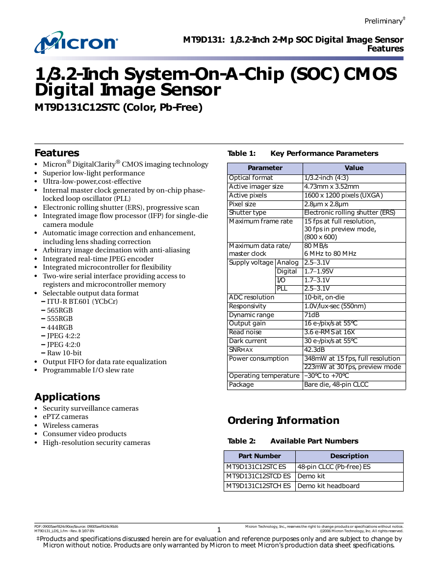
1/3.2-Inch System-On-A-Chip (SOC) CMOS
Digital Image Sensor
MT9D131C12STC (Color, Pb-Free)
Features
• Micron® DigitalClarity® CMOS imaging technology
Superior low-light performance
Ultra-low-power,cost-effective
Internal master clock generated by on-chip phase-
locked loop oscillator (PLL)
Electronic rolling shutter (ERS), progressive scan
Integrated image flow processor (IFP) for single-die
camera module
Automatic image correction and enhancement,
including lens shading correction
Arbitrary image decimation with anti-aliasing
Integrated real-time JPEG encoder
Integrated microcontroller for flexibility
Two-wire serial interface providing access to
registers and microcontroller memory
Selectable output data format
– ITU-R BT.601 (YCbCr)
– 565RGB
– 555RGB
– 444RGB
– JPEG 4:2:2
– JPEG 4:2:0
– Raw 10-bit
Output FIFO for data rate equalization
Programmable I/O slew rate
Applications
Security surveillance cameras
ePTZ cameras
Wireless cameras
Consumer video products
High-resolution security cameras
Table 1:
Key Performance Parameters
Parameter
Optical format
Active imager size
Active pixels
Pixel size
Shutter type
Maximum frame rate
Value
1/3.2-inch (4:3)
4.73mm x 3.52mm
1600 x 1200 pixels (UXGA)
2.8µm x 2.8µm
Electronic rolling shutter (ERS)
15 fps at full resolution,
30 fps in preview mode,
(800 x 600)
80 MB/s
6 MHz to 80 MHz
Digital
I/O
PLL
Maximum data rate/
master clock
Supply voltage Analog 2.5−3.1V
1.7−1.95V
1.7−3.1V
2.5−3.1V
10-bit, on-die
1.0V/lux-sec (550nm)
71dB
16 e-/pix/s at 55°C
3.6 e-RMS at 16X
30 e-/pix/s at 55°C
42.3dB
348mW at 15 fps, full resolution
223mW at 30 fps, preview mode
ADC resolution
Responsivity
Dynamic range
Output gain
Read noise
Dark current
SNRMAX
Power consumption
Operating temperature –30°C to +70°C
Package
Bare die, 48-pin CLCC
Ordering Information
Table 2:
Available Part Numbers
Part Number
Description
48-pin CLCC (Pb-free) ES
MT9D131C12STC ES
MT9D131C12STCD ES Demo kit
MT9D131C12STCH ES Demo kit headboard
PDF: 09005aef824c90ce/Source: 09005aef824c90d6
Micron Technology, Inc., reserves the right to change products or specifications without notice.
MT9D131_LDS_1.fm - Rev. B 3/07 EN
©2006 Micron Technology, Inc. All rights reserved.
‡Products and specifications discussed herein are for evaluation and reference purposes only and are subject to change by
Micron without notice. Products are only warranted by Micron to meet Micron’s production data sheet specifications.
1
�
MT9D131: 1/3.2-Inch 2-Mp SOC Digital Image Sensor
General Description
Preliminary
General Description
Micron Imaging MT9D131 is a 1/3.2 inch, 2-megapixel CMOS image sensor with an inte-
grated advanced camera system. The camera system features a microcontroller (MCU)
and a sophisticated image flow processor (IFP) with a real-time JPEG encoder.
The sensor core consists of an active pixel array of 1668 x 1248 pixels, programmable
timing and control circuitry including a PLL, analog signal chain with automatic offset
correction and programmable gain, and two 10-bit A/D converters (ADC). The entire
system-on-a-chip (SOC) has ultra-low power requirements and superior low-light per-
formance that is particularly suitable for a wide variety of applications.
Feature Overview
The MT9D131 is a color image sensor with a Bayer color filter arrangement.
The MT9D131 has an embedded phase-locked loop oscillator (PLL) that can be used
with the common wireless system clock. When in use, the PLL adjusts the incoming
clock frequency, allowing the MT9D131 to run at almost any resolution and frame rate.
To reduce power consumption, the PLL can be bypassed and powered down. The
MT9D131 has numerous power conserving features, including an ultra-low power
standby mode and the ability to individually shut down unused digital blocks.
Another important consideration for wireless devices is their electromagnetic emission
or interference (EMI). The MT9D131 has a programmable I/O slew rate to minimize its
EMI and an output FIFO to eliminate output data bursts.
The advanced IFP and flexible programmability of the MT9D131 provide a variety of
ways to enhance and optimize the image sensor performance. Built-in optimization
algorithms enable the MT9D131 to operate at factory settings as a fully automatic, highly
adaptable camera. However, most of its settings are user-programmable by changing
register values.
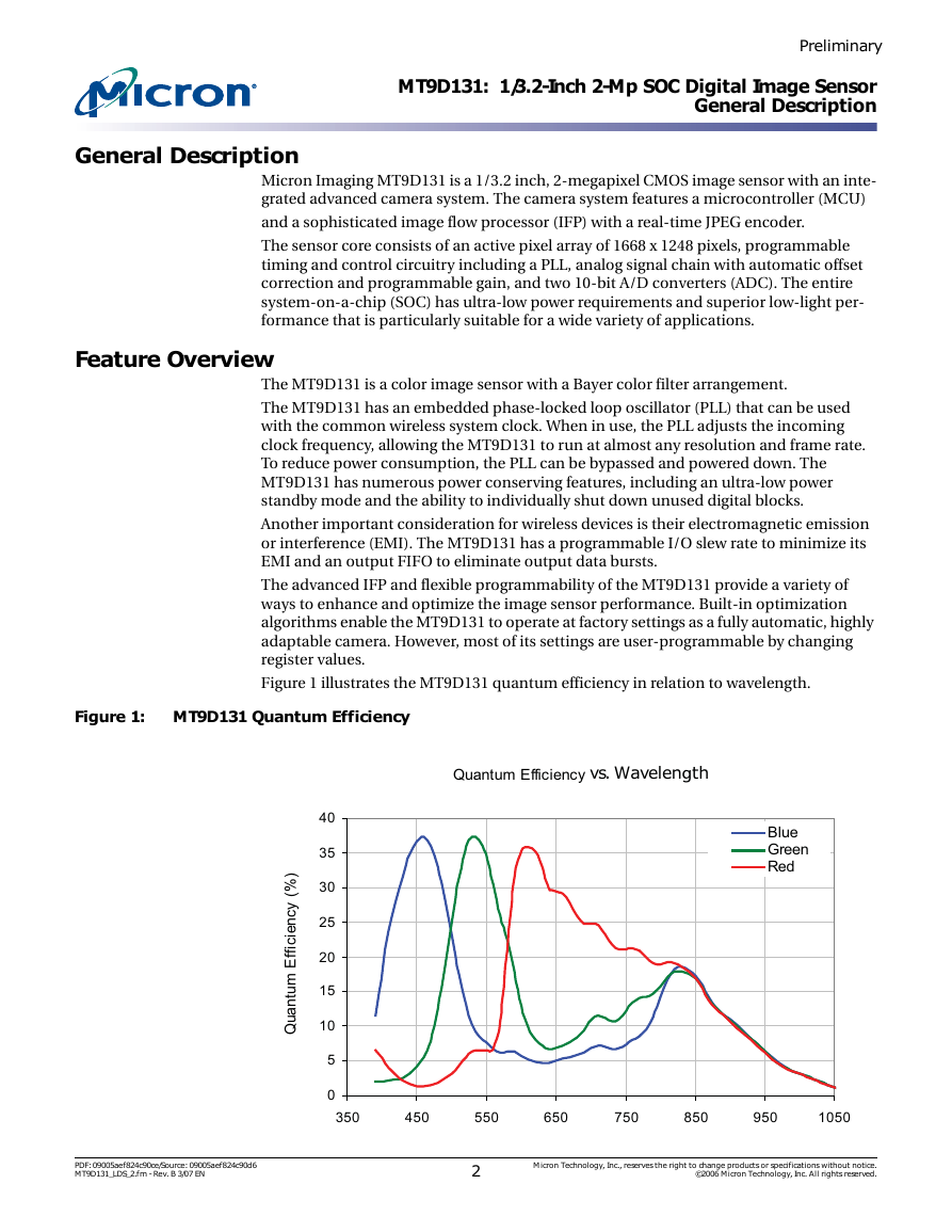
Figure 1 illustrates the MT9D131 quantum efficiency in relation to wavelength.
Figure 1:
MT9D131 Quantum Efficiency
Quantum Efficiency
vs. Wavelength
Blue
Green
Red
40
35
30
25
20
15
10
5
0
)
%
(
y
c
n
e
c
i
i
f
f
E
m
u
t
n
a
u
Q
350
450
550
650
750
850
950
1050
PDF: 09005aef824c90ce/Source: 09005aef824c90d6
MT9D131_LDS_2.fm - Rev. B 3/07 EN
2
Micron Technology, Inc., reserves the right to change products or specifications without notice.
©2006 Micron Technology, Inc. All rights reserved.
�
MT9D131: 1/3.2-Inch 2-Mp SOC Digital Image Sensor
Typical Connection
Preliminary
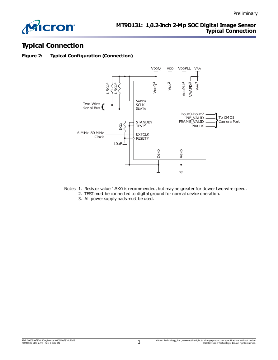
Typical Connection
Figure 2:
Typical Configuration (Connection)
VDDQ
VDD
VDDPLL
VAA
1
Ω
K
5
.
1
1
Ω
K
5
.
1
3
Q
D
D
V
3
D
D
V
3
A
A
V
3
L
L
P
D
D
V
I
3
X
P
A
A
V
Two-Wire
Serial Bus
6 MHz–80 MHz
Clock
Ω
K
1
10µF
SADDR
SCLK
SDATA
STANDBY
TEST2
EXTCLK
RESET#
DOUT0-DOUT7
LINE_VALID
FRAME_VALID
PIXCLK
To CMOS
Camera Port
D
N
G
D
D
N
G
A
Notes: 1. Resistor value 1.5KΩ is recommended, but may be greater for slower two-wire speed.
2. TEST must be connected to digital ground for normal device operation.
3. All power supply pads must be used.
PDF: 09005aef824c90ce/Source: 09005aef824c90d6
MT9D131_LDS_2.fm - Rev. B 3/07 EN
3
Micron Technology, Inc., reserves the right to change products or specifications without notice.
©2006 Micron Technology, Inc. All rights reserved.
�
MT9D131: 1/3.2-Inch 2-Mp SOC Digital Image Sensor
Signal Description
Preliminary
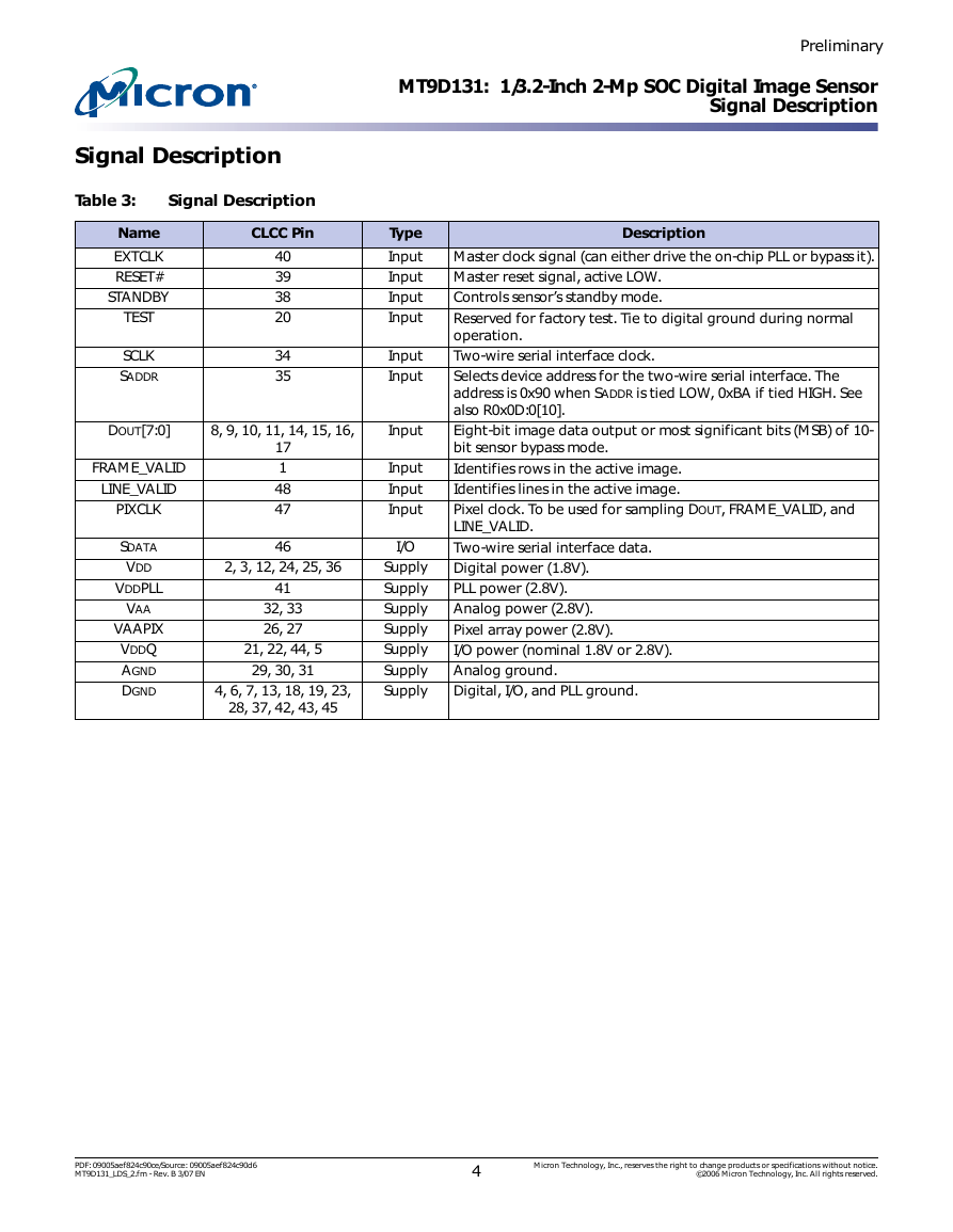
Signal Description
Table 3:
Signal Description
Name
EXTCLK
RESET#
STANDBY
TEST
SCLK
SADDR
CLCC Pin
40
39
38
20
34
35
Type
Input
Input
Input
Input
Input
Input
DOUT[7:0]
8, 9, 10, 11, 14, 15, 16,
Input
FRAME_VALID
LINE_VALID
PIXCLK
SDATA
VDD
VDDPLL
VAA
VAAPIX
VDDQ
AGND
DGND
17
1
48
47
46
2, 3, 12, 24, 25, 36
41
32, 33
26, 27
21, 22, 44, 5
29, 30, 31
4, 6, 7, 13, 18, 19, 23,
28, 37, 42, 43, 45
Input
Input
Input
I/O
Supply
Supply
Supply
Supply
Supply
Supply
Supply
Description
Master clock signal (can either drive the on-chip PLL or bypass it).
Master reset signal, active LOW.
Controls sensor’s standby mode.
Reserved for factory test. Tie to digital ground during normal
operation.
Two-wire serial interface clock.
Selects device address for the two-wire serial interface. The
address is 0x90 when SADDR is tied LOW, 0xBA if tied HIGH. See
also R0x0D:0[10].
Eight-bit image data output or most significant bits (MSB) of 10-
bit sensor bypass mode.
Identifies rows in the active image.
Identifies lines in the active image.
Pixel clock. To be used for sampling DOUT, FRAME_VALID, and
LINE_VALID.
Two-wire serial interface data.
Digital power (1.8V).
PLL power (2.8V).
Analog power (2.8V).
Pixel array power (2.8V).
I/O power (nominal 1.8V or 2.8V).
Analog ground.
Digital, I/O, and PLL ground.
PDF: 09005aef824c90ce/Source: 09005aef824c90d6
MT9D131_LDS_2.fm - Rev. B 3/07 EN
4
Micron Technology, Inc., reserves the right to change products or specifications without notice.
©2006 Micron Technology, Inc. All rights reserved.
�
MT9D131: 1/3.2-Inch 2-Mp SOC Digital Image Sensor
Signal Description
Preliminary
Figure 3:
48-Pin CLCC Pinout
D
N
G
D
Q
D
D
V
D
N
G
D
D
D
V
D
D
V
D
I
L
A
V
_
E
M
A
R
F
D
I
L
A
V
_
E
N
I
L
K
L
C
X
P
I
A
T
A
D
S
D
N
G
D
Q
D
D
V
D
N
G
D
DGND
DOUT7
DOUT6
DOUT5
DOUT4
VDD
DGND
DOUT3
DOUT2
DOUT1
DOUT0
DGND
7
8
9
10
11
12
13
14
15
16
17
18
6
5
4
3
2
1
48
47
46
45
44
43
42
41
40
39
38
37
36
35
34
33
32
31
19
20
21
22
23
24
25
26
27
28
29
30
D
N
G
D
T
S
E
T
Q
D
D
V
Q
D
D
V
D
N
G
D
D
D
V
D
D
V
D
N
G
D
D
N
G
A
D
N
G
A
I
X
P
A
A
V
I
X
P
A
A
V
DGND
VDDPLL
EXTCLK
RESET#
STANDBY
DGND
VDD
SADDR
SCLK
VAA
VAA
AGND
PDF: 09005aef824c90ce/Source: 09005aef824c90d6
MT9D131_LDS_2.fm - Rev. B 3/07 EN
5
Micron Technology, Inc., reserves the right to change products or specifications without notice.
©2006 Micron Technology, Inc. All rights reserved.
�
MT9D131: 1/3.2-Inch 2-Mp SOC Digital Image Sensor
Architecture Overview
Preliminary
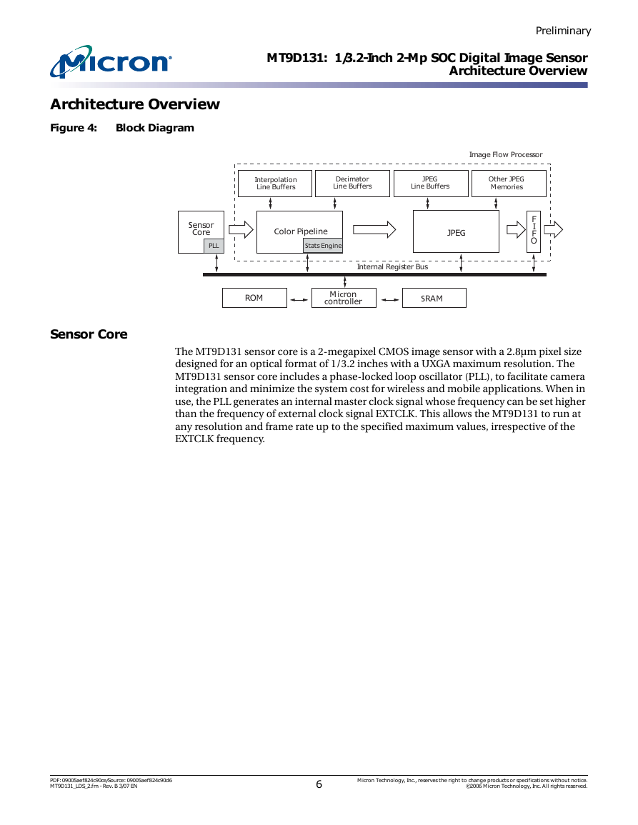
Architecture Overview
Figure 4:
Block Diagram
Interpolation
Line Buffers
Decimator
Line Buffers
JPEG
Line Buffers
Other JPEG
Memories
Image Flow Processor
Sensor
Core
PLL
Color Pipeline
Stats Engine
JPEG
F
I
F
O
Internal Register Bus
ROM
Micron
controller
SRAM
Sensor Core
The MT9D131 sensor core is a 2-megapixel CMOS image sensor with a 2.8µm pixel size
designed for an optical format of 1/3.2 inches with a UXGA maximum resolution. The
MT9D131 sensor core includes a phase-locked loop oscillator (PLL), to facilitate camera
integration and minimize the system cost for wireless and mobile applications. When in
use, the PLL generates an internal master clock signal whose frequency can be set higher
than the frequency of external clock signal EXTCLK. This allows the MT9D131 to run at
any resolution and frame rate up to the specified maximum values, irrespective of the
EXTCLK frequency.
PDF: 09005aef824c90ce/Source: 09005aef824c90d6
MT9D131_LDS_2.fm - Rev. B 3/07 EN
6
Micron Technology, Inc., reserves the right to change products or specifications without notice.
©2006 Micron Technology, Inc. All rights reserved.
�
MT9D131: 1/3.2-Inch 2-Mp SOC Digital Image Sensor
Architecture Overview
Preliminary
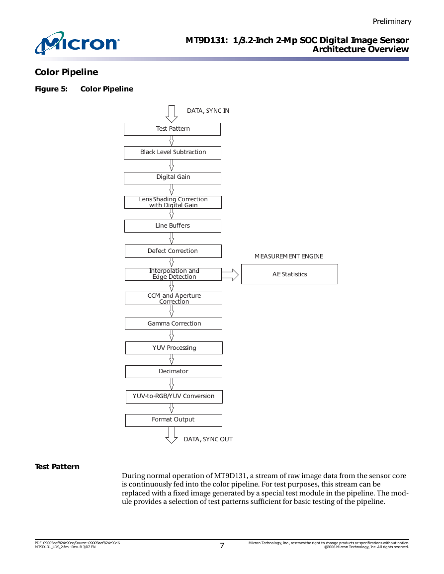
Color Pipeline
Figure 5:
Color Pipeline
DATA, SYNC IN
Test Pattern
Black Level Subtraction
Digital Gain
Lens Shading Correction
with Digital Gain
Line Buffers
Defect Correction
Interpolation and
Edge Detection
CCM and Aperture
Correction
Gamma Correction
YUV Processing
Decimator
YUV-to-RGB/YUV Conversion
Format Output
DATA, SYNC OUT
MEASUREMENT ENGINE
AE Statistics
Test Pattern
During normal operation of MT9D131, a stream of raw image data from the sensor core
is continuously fed into the color pipeline. For test purposes, this stream can be
replaced with a fixed image generated by a special test module in the pipeline. The mod-
ule provides a selection of test patterns sufficient for basic testing of the pipeline.
PDF: 09005aef824c90ce/Source: 09005aef824c90d6
MT9D131_LDS_2.fm - Rev. B 3/07 EN
7
Micron Technology, Inc., reserves the right to change products or specifications without notice.
©2006 Micron Technology, Inc. All rights reserved.
�
MT9D131: 1/3.2-Inch 2-Mp SOC Digital Image Sensor
Architecture Overview
Preliminary
Black Level Conditioning and Digital Gain
Image stream processing starts with black level conditioning and multiplication of all
pixel values by a programmable digital gain.
Lens Shading Correction
Line Buffers
Defect Correction
Inexpensive lenses tend to produce images whose brightness is significantly attenuated
near the edges. Chromatic aberration in such lenses can cause color variation across the
field of view. There are also other factors causing fixed-pattern signal gradients in
images captured by image sensors. The cumulative result of all these factors is known as
lens shading. The MT9D131 has an embedded lens shading correction (LC) module that
can be programmed to precisely counter the shading effect of a lens on each RGB color
signal. The LC module multiplies RGB signals by a 2-dimensional correction function
F(x,y), whose profile in both x and y direction is a piecewise quadratic polynomial with
coefficients independently programmable for each direction and color.
Several data processing steps following the lens shading correction require access to
pixel values from up to 8 consecutive image lines. For these lines to be simultaneously
available for processing, they must be buffered. The IFP includes a number of SRAM line
buffers that are used to perform defect correction, color interpolation, image decima-
tion, and JPEG encoding.
The IFP performs on-the-fly defect correction that can mask pixel array defects such as
high-dark-current (“hot”) pixels and pixels that are darker or brighter than their neigh-
bors due to photoresponse nonuniformity. The defect correction algorithm uses several
pixel features to distinguish between normal and defective pixels. After identifying the
latter, it replaces their actual values with values inferred from the values of nearest
same-color neighbors.
Color Interpolation and Edge Detection
In the raw data stream fed by the sensor core to the IFP, each pixel is represented by a
10-bit integer number, which, to make things simple, can be considered proportional to
the pixel’s response to a one-color light stimulus—red, green, or blue—depending on
the pixel’s position under the color filter array. Initial data processing steps, up to and
including the defect correction, preserve the one-color-per-pixel nature of the data
stream, but after the defect correction it must be converted to a three-colors-per-pixel
stream appropriate for standard color processing. The conversion is done by an edge-
sensitive color interpolation module. The module pads the incomplete color informa-
tion available for each pixel with information extracted from an appropriate set of
neighboring pixels. The algorithm used to select this set and extract the information
seeks the best compromise between maintaining the sharpness of the image and filter-
ing out high-frequency noise. The simplest interpolation algorithm is to sort the nearest
eight neighbors of every pixel into three sets—red, green, and blue, discard the set of
pixels of the same color as the center pixel (if there are any), calculate average pixel val-
ues for the remaining two sets, and use the averages instead of the missing color data for
the center pixel. Such averaging reduces high-frequency noise, but it also blurs and dis-
torts sharp transitions (edges) in the image. To avoid this problem, the interpolation
module performs edge detection in the neighborhood of every processed pixel and,
depending on its results, extracts color information from neighboring pixels in a number
of different ways. In effect, it does low-pass filtering in flat-field image areas and avoids
doing it near edges.
PDF: 09005aef824c90ce/Source: 09005aef824c90d6
MT9D131_LDS_2.fm - Rev. B 3/07 EN
8
Micron Technology, Inc., reserves the right to change products or specifications without notice.
©2006 Micron Technology, Inc. All rights reserved.
�



 2023年江西萍乡中考道德与法治真题及答案.doc
 2012年重庆南川中考生物真题及答案.doc
 2013年江西师范大学地理学综合及文艺理论基础考研真题.doc
 2020年四川甘孜小升初语文真题及答案I卷.doc
 2020年注册岩土工程师专业基础考试真题及答案.doc
 2023-2024学年福建省厦门市九年级上学期数学月考试题及答案.doc
 2021-2022学年辽宁省沈阳市大东区九年级上学期语文期末试题及答案.doc
 2022-2023学年北京东城区初三第一学期物理期末试卷及答案.doc
 2018上半年江西教师资格初中地理学科知识与教学能力真题及答案.doc
 2012年河北国家公务员申论考试真题及答案-省级.doc
 2020-2021学年江苏省扬州市江都区邵樊片九年级上学期数学第一次质量检测试题及答案.doc
 2022下半年黑龙江教师资格证中学综合素质真题及答案.doc