PS7516
PS7516
Description
Description
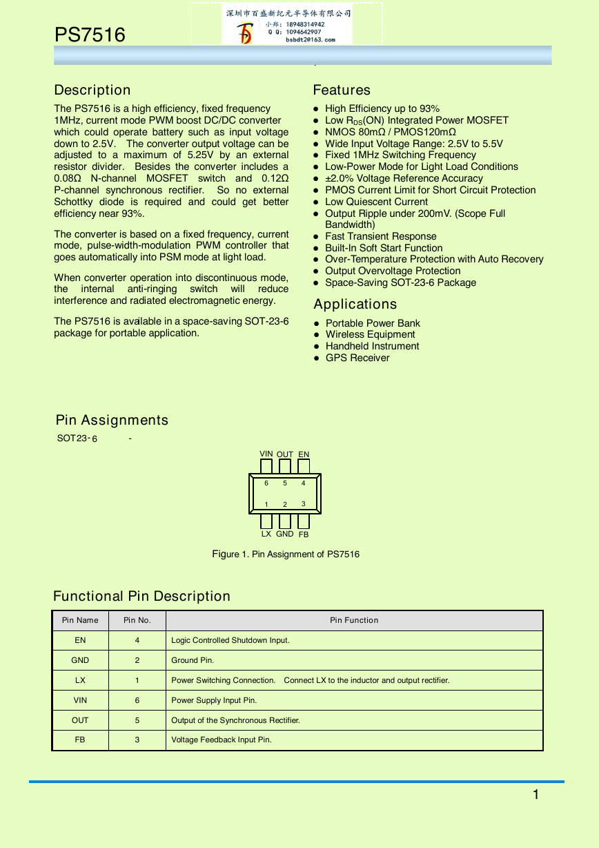
The PS7516 is a high efficiency, fixed frequency
The PS7516 is a high efficiency, fixed frequency
1MHz, current mode PWM boost DC/DC converter
1MHz, current mode PWM boost DC/DC converter
which could operate battery such as input voltage
which could operate battery such as input voltage
down to 2.5V. The converter output voltage can be
down to 2.5V. The converter output voltage can be
adjusted to a maximum of 5.25V by an external
adjusted to a maximum of 5.25V by an external
resistor divider. Besides the converter includes a
resistor divider. Besides the converter includes a
0.08Ω N-channel MOSFET switch and 0.12Ω
0.08Ω N-channel MOSFET switch and 0.12Ω
P-channel synchronous rectifier. So no external
P-channel synchronous rectifier. So no external
Schottky diode is required and could get better
Schottky diode is required and could get better
efficiency near 93%.
efficiency near 93%.
The converter is based on a fixed frequency, current
The converter is based on a fixed frequency, current
mode, pulse-width-modulation PWM controller that
mode, pulse-width-modulation PWM controller that
goes automatically into PSM mode at light load.
goes automatically into PSM mode at light load.
When converter operation into discontinuous mode,
When converter operation into discontinuous mode,
the
reduce
the
reduce
interference and radiated electromagnetic energy.
interference and radiated electromagnetic energy.
internal anti-ringing
internal anti-ringing
switch will
switch will
The PS7516 is available in a space-saving SOT-23-6
The PS7516 is available in a space-saving SOT-23-6
package for portable application.
package for portable application.
Pin Assignments
Pin Assignments
SOT
SOT
23- 6
23- 6
-
-
.
.
Features
Features
Fixed 1MHz Switching Frequency
High Efficiency up to 93%
High Efficiency up to 93%
Low RDS(ON) Integrated Power MOSFET
Low RDS(ON) Integrated Power MOSFET
NMOS 80mΩ / PMOS120mΩ
NMOS 80mΩ / PMOS120mΩ
Wide Input Voltage Range: 2.5V to 5.5V
Wide Input Voltage Range: 2.5V to 5.5V
Fixed 1MHz Switching Frequency
Low-Power Mode for Light Load Conditions
Low-Power Mode for Light Load Conditions
±2.0% Voltage Reference Accuracy
±2.0% Voltage Reference Accuracy
PMOS Current Limit for Short Circuit Protection
PMOS Current Limit for Short Circuit Protection
Low Quiescent Current
Low Quiescent Current
Output Ripple under 200mV. (Scope Full
Output Ripple under 200mV. (Scope Full
Bandwidth)
Bandwidth)
Fast Transient Response
Fast Transient Response
Built-In Soft Start Function
Built-In Soft Start Function
Over-Temperature Protection with Auto Recovery
Over-Temperature Protection with Auto Recovery
Output Overvoltage Protection
Output Overvoltage Protection
Space-Saving SOT-23-6 Package
Space-Saving SOT-23-6 Package
Applications
Applications
Portable Power Bank
Portable Power Bank
Wireless Equipment
Wireless Equipment
Handheld Instrument
Handheld Instrument
GPS Receiver
GPS Receiver
VIN
VIN
OUT EN
OUT EN
6
6
1
1
5
5
2
2
4
4
3
3
LX
LX
GND
GND
FB
FB
Figure 1. Pin Assignment of PS7516
Figure 1. Pin Assignment of PS7516
Functional Pin Description
Functional Pin Description
Pin Name
Pin Name
Pin No.
Pin No.
Pin Function
Pin Function
EN
EN
GND
GND
LX
LX
VIN
VIN
OUT
OUT
FB
FB
4
4
2
2
1
1
6
6
5
5
3
3
Logic Controlled Shutdown Input.
Logic Controlled Shutdown Input.
Ground Pin.
Ground Pin.
Power Switching Connection. Connect LX to the inductor and output rectifier.
Power Switching Connection. Connect LX to the inductor and output rectifier.
Power Supply Input Pin.
Power Supply Input Pin.
Output of the Synchronous Rectifier.
Output of the Synchronous Rectifier.
Voltage Feedback Input Pin.
Voltage Feedback Input Pin.
1
1
�
PS7516
PS7516
.
.
85T
85T
Block Diagram
Block Diagram
VIN
VIN
LX
LX
EN
EN
On/Off
On/Off
Control
Control
ANTI-RING
ANTI-RING
PMOS
PMOS
NMOS
NMOS
OUT
OUT
Body-Diode
Body-Diode
Switch
Switch
Isense/Current Limit
Isense/Current Limit
Slope Comp.
Slope Comp.
Anti-Reverse
Anti-Reverse
Comparator
Comparator
COMP
COMP
OTP
OTP
Error
Error
Amp
Amp
Bandgap
Bandgap
Reference
Reference
FB
FB
PWM
PWM
Control
Control
Logic
Logic
PFM
PFM
Control
Control
OSC
OSC
OVP
OVP
UVLO
UVLO
VIN
VIN
GND
GND
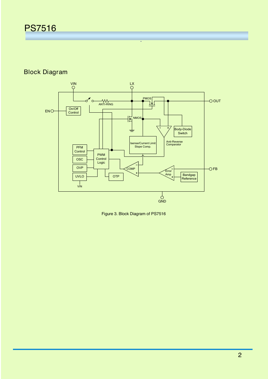
Figure 3. Block Diagram of PS7516
Figure 3. Block Diagram of PS7516
85T
85T
2
2
�
PS7516
PS7516
Typical Application Circuit
Typical Application Circuit
VIN
VIN
2.5V to 5.5V
2.5V to 5.5V
C1
C1
10μF
10μF
C2
C2
0.1μF
0.1μF
L1
L1
10μH
10μH
6
6
2
2
4
4
VIN
VIN
LX
LX
PS7516
PS7516
GND
GND
OUT
OUT
EN
EN
FB
FB
1
1
5
5
3
3
C4, C6
C6
0.1μF
0.1μF
C5
C , C5
22μF
22μF
ON
ON
OFF
OFF
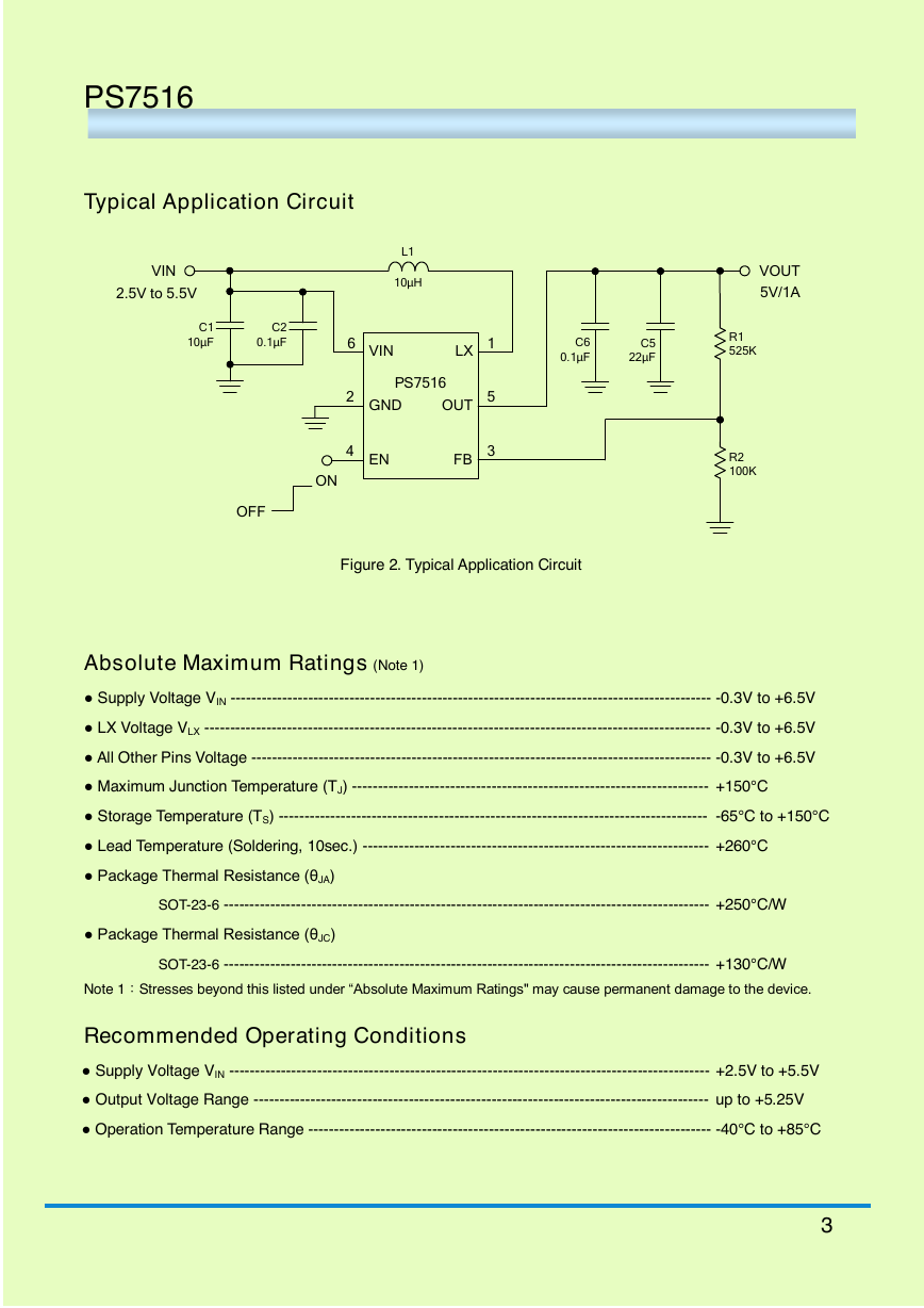
Figure 2. Typical Application Circuit
Figure 2. Typical Application Circuit
VOUT
VOUT
5V/1A
5V/1A
R1
R1
525K
525K
R2
R2
100K
100K
85T
85T
Absolute Maximum Ratings (Note 1)
Absolute Maximum Ratings (Note 1)
● Supply Voltage VIN --------------------------------------------------------------------------------------------- -0.3V to +6.5V
● Supply Voltage VIN --------------------------------------------------------------------------------------------- -0.3V to +6.5V
● LX Voltage VLX -------------------------------------------------------------------------------------------------- -0.3V to +6.5V
● LX Voltage VLX -------------------------------------------------------------------------------------------------- -0.3V to +6.5V
● All Other Pins Voltage ----------------------------------------------------------------------------------------- -0.3V to +6.5V
● All Other Pins Voltage ----------------------------------------------------------------------------------------- -0.3V to +6.5V
● Maximum Junction Temperature (TJ) --------------------------------------------------------------------- +150°C
● Maximum Junction Temperature (TJ) --------------------------------------------------------------------- +150°C
● Storage Temperature (TS) ----------------------------------------------------------------------------------- -65°C to +150°C
● Storage Temperature (TS) ----------------------------------------------------------------------------------- -65°C to +150°C
● Lead Temperature (Soldering, 10sec.) ------------------------------------------------------------------- +260°C
● Lead Temperature (Soldering, 10sec.) ------------------------------------------------------------------- +260°C
● Package Thermal Resistance (θJA)
● Package Thermal Resistance (θJA)
SOT-23-6 ---------------------------------------------------------------------------------------------- +250°C/W
SOT-23-6 ---------------------------------------------------------------------------------------------- +250°C/W
● Package Thermal Resistance (θJC)
● Package Thermal Resistance (θJC)
SOT-23-6 ---------------------------------------------------------------------------------------------- +130°C/W
SOT-23-6 ---------------------------------------------------------------------------------------------- +130°C/W
Note 1:Stresses beyond this listed under “Absolute Maximum Ratings" may cause permanent damage to the device.
Note 1:Stresses beyond this listed under “Absolute Maximum Ratings" may cause permanent damage to the device.
Recommended Operating Conditions
Recommended Operating Conditions
● Supply Voltage VIN --------------------------------------------------------------------------------------------- +2.5V to +5.5V
● Supply Voltage VIN --------------------------------------------------------------------------------------------- +2.5V to +5.5V
● Output Voltage Range ---------------------------------------------------------------------------------------- up to +5.25V
● Output Voltage Range ---------------------------------------------------------------------------------------- up to +5.25V
● Operation Temperature Range ------------------------------------------------------------------------------ -40°C to +85°C
● Operation Temperature Range ------------------------------------------------------------------------------ -40°C to +85°C
3
3
�
PS7516
PS7516
Electrical Characteristics
Electrical Characteristics
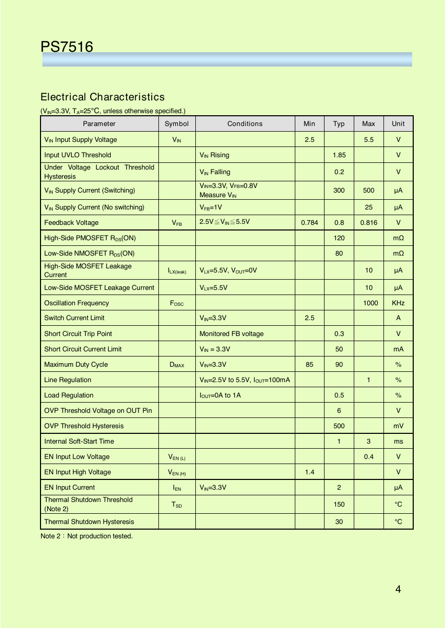
(VIN=3.3V, TA=25°C, unless otherwise specified.)
(VIN=3.3V, TA=25°C, unless otherwise specified.)
85T
85T
Parameter
Parameter
Symbol
Symbol
Conditions
Conditions
Min
Min
Typ
Typ
Max
Max
Unit
Unit
VIN Input Supply Voltage
VIN Input Supply Voltage
VIN
VIN
2.5
2.5
5.5
5.5
Input UVLO Threshold
Input UVLO Threshold
Under Voltage Lockout Threshold
Under Voltage Lockout Threshold
Hysteresis
Hysteresis
VIN Supply Current (Switching)
VIN Supply Current (Switching)
VIN Supply Current (No switching)
VIN Supply Current (No switching)
VIN Rising
VIN Rising
VIN Falling
VIN Falling
VIN=3.3V, VFB=0.8V
VIN=3.3V, VFB=0.8V
Measure VIN
Measure VIN
VFB=1V
VFB=1V
1.85
1.85
0.2
0.2
300
300
500
500
25
25
V
V
V
V
V
V
μA
μA
μA
μA
Feedback Voltage
Feedback Voltage
VFB
VFB
2.5V≦VIN≦5.5V
2.5V≦VIN≦5.5V
0.784
0.784
0.8
0.8
0.816
0.816
V
V
High-Side PMOSFET RDS(ON)
High-Side PMOSFET RDS(ON)
Low-Side NMOSFET RDS(ON)
Low-Side NMOSFET RDS(ON)
High-Side MOSFET Leakage
High-Side MOSFET Leakage
Current
Current
ILX(leak)
ILX(leak)
VLX=5.5V, VOUT=0V
VLX=5.5V, VOUT=0V
Low-Side MOSFET Leakage Current
Low-Side MOSFET Leakage Current
VLX=5.5V
VLX=5.5V
Oscillation Frequency
Oscillation Frequency
FOSC
FOSC
Switch Current Limit
Switch Current Limit
Short Circuit Trip Point
Short Circuit Trip Point
Short Circuit Current Limit
Short Circuit Current Limit
VIN=3.3V
VIN=3.3V
Monitored FB voltage
Monitored FB voltage
VIN = 3.3V
VIN = 3.3V
Maximum Duty Cycle
Maximum Duty Cycle
DMAX
DMAX
VIN=3.3V
VIN=3.3V
Line Regulation
Line Regulation
Load Regulation
Load Regulation
OVP Threshold Voltage on OUT Pin
OVP Threshold Voltage on OUT Pin
OVP Threshold Hysteresis
OVP Threshold Hysteresis
Internal Soft-Start Time
Internal Soft-Start Time
EN Input Low Voltage
EN Input Low Voltage
EN Input High Voltage
EN Input High Voltage
VEN (L)
VEN (L)
VEN (H)
VEN (H)
VIN=2.5V to 5.5V, IOUT=100mA
VIN=2.5V to 5.5V, IOUT=100mA
IOUT=0A to 1A
IOUT=0A to 1A
EN Input Current
EN Input Current
IEN
IEN
VIN=3.3V
VIN=3.3V
Thermal Shutdown Threshold
Thermal Shutdown Threshold
(Note 2)
(Note 2)
Thermal Shutdown Hysteresis
Thermal Shutdown Hysteresis
Note 2:Not production tested.
Note 2:Not production tested.
TSD
TSD
450
2.5
2.5
85
85
1.4
1.4
1000
KHz
KHz
120
120
80
80
0.3
0.3
50
50
90
90
0.5
0.5
6
6
500
500
1
1
2
2
150
150
30
30
10
10
10
10
mΩ
mΩ
mΩ
mΩ
μA
μA
μA
μA
1
1
3
3
0.4
0.4
A
A
V
V
mA
mA
%
%
%
%
%
%
V
V
mV
mV
ms
ms
V
V
V
V
μA
μA
°C
°C
°C
°C
4
4
�
PS7516
PS7516
Application Information
Application Information
Controller Circuit
Controller Circuit
Device Enable
Device Enable
85T
85T
constant
constant
to regulate
to regulate
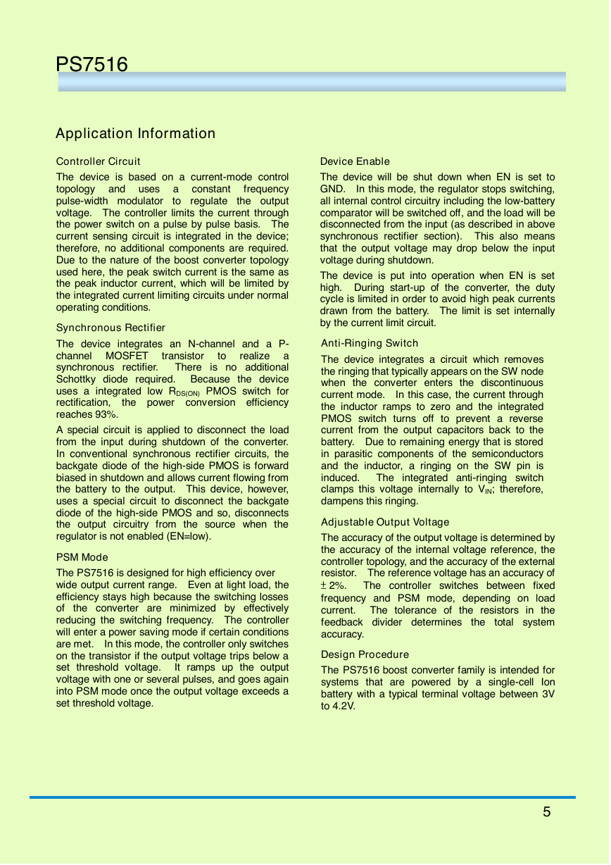
The device is based on a current-mode control
The device is based on a current-mode control
topology and uses a
topology and uses a
frequency
frequency
pulse-width modulator
the output
the output
pulse-width modulator
voltage. The controller limits the current through
voltage. The controller limits the current through
the power switch on a pulse by pulse basis. The
the power switch on a pulse by pulse basis. The
current sensing circuit is integrated in the device;
current sensing circuit is integrated in the device;
therefore, no additional components are required.
therefore, no additional components are required.
Due to the nature of the boost converter topology
Due to the nature of the boost converter topology
used here, the peak switch current is the same as
used here, the peak switch current is the same as
the peak inductor current, which will be limited by
the peak inductor current, which will be limited by
the integrated current limiting circuits under normal
the integrated current limiting circuits under normal
operating conditions.
operating conditions.
Synchronous Rectifier
Synchronous Rectifier
transistor
transistor
The device integrates an N-channel and a P-
The device integrates an N-channel and a P-
channel MOSFET
realize a
channel MOSFET
realize a
synchronous rectifier. There is no additional
synchronous rectifier. There is no additional
Schottky diode required. Because the device
Schottky diode required. Because the device
uses a integrated low RDS(ON) PMOS switch for
uses a integrated low RDS(ON) PMOS switch for
rectification,
the power conversion efficiency
rectification,
the power conversion efficiency
reaches 93%.
reaches 93%.
to
to
A special circuit is applied to disconnect the load
A special circuit is applied to disconnect the load
from the input during shutdown of the converter.
from the input during shutdown of the converter.
In conventional synchronous rectifier circuits, the
In conventional synchronous rectifier circuits, the
backgate diode of the high-side PMOS is forward
backgate diode of the high-side PMOS is forward
biased in shutdown and allows current flowing from
biased in shutdown and allows current flowing from
the battery to the output. This device, however,
the battery to the output. This device, however,
uses a special circuit to disconnect the backgate
uses a special circuit to disconnect the backgate
diode of the high-side PMOS and so, disconnects
diode of the high-side PMOS and so, disconnects
the output circuitry from the source when the
the output circuitry from the source when the
regulator is not enabled (EN=low).
regulator is not enabled (EN=low).
PSM Mode
PSM Mode
The PS7516 is designed for high efficiency over
The PS7516 is designed for high efficiency over
wide output current range. Even at light load, the
wide output current range. Even at light load, the
efficiency stays high because the switching losses
efficiency stays high because the switching losses
of the converter are minimized by effectively
of the converter are minimized by effectively
reducing the switching frequency. The controller
reducing the switching frequency. The controller
will enter a power saving mode if certain conditions
will enter a power saving mode if certain conditions
are met. In this mode, the controller only switches
are met. In this mode, the controller only switches
on the transistor if the output voltage trips below a
on the transistor if the output voltage trips below a
set threshold voltage. It ramps up the output
set threshold voltage. It ramps up the output
voltage with one or several pulses, and goes again
voltage with one or several pulses, and goes again
into PSM mode once the output voltage exceeds a
into PSM mode once the output voltage exceeds a
set threshold voltage.
set threshold voltage.
The device will be shut down when EN is set to
The device will be shut down when EN is set to
GND. In this mode, the regulator stops switching,
GND. In this mode, the regulator stops switching,
all internal control circuitry including the low-battery
all internal control circuitry including the low-battery
comparator will be switched off, and the load will be
comparator will be switched off, and the load will be
disconnected from the input (as described in above
disconnected from the input (as described in above
synchronous rectifier section). This also means
synchronous rectifier section). This also means
that the output voltage may drop below the input
that the output voltage may drop below the input
voltage during shutdown.
voltage during shutdown.
The device is put into operation when EN is set
The device is put into operation when EN is set
high. During start-up of the converter, the duty
high. During start-up of the converter, the duty
cycle is limited in order to avoid high peak currents
cycle is limited in order to avoid high peak currents
drawn from the battery. The limit is set internally
drawn from the battery. The limit is set internally
by the current limit circuit.
by the current limit circuit.
Anti-Ringing Switch
Anti-Ringing Switch
The device integrates a circuit which removes
The device integrates a circuit which removes
the ringing that typically appears on the SW node
the ringing that typically appears on the SW node
when the converter enters the discontinuous
when the converter enters the discontinuous
current mode. In this case, the current through
current mode. In this case, the current through
the inductor ramps to zero and the integrated
the inductor ramps to zero and the integrated
PMOS switch turns off to prevent a reverse
PMOS switch turns off to prevent a reverse
current from the output capacitors back to the
current from the output capacitors back to the
battery. Due to remaining energy that is stored
battery. Due to remaining energy that is stored
in parasitic components of the semiconductors
in parasitic components of the semiconductors
and the inductor, a ringing on the SW pin is
and the inductor, a ringing on the SW pin is
induced. The integrated anti-ringing switch
induced. The integrated anti-ringing switch
clamps this voltage internally to VIN; therefore,
clamps this voltage internally to VIN; therefore,
dampens this ringing.
dampens this ringing.
Adjustable Output Voltage
Adjustable Output Voltage
The accuracy of the output voltage is determined by
The accuracy of the output voltage is determined by
the accuracy of the internal voltage reference, the
the accuracy of the internal voltage reference, the
controller topology, and the accuracy of the external
controller topology, and the accuracy of the external
resistor. The reference voltage has an accuracy of
resistor. The reference voltage has an accuracy of
± 2%. The controller switches between fixed
± 2%. The controller switches between fixed
frequency and PSM mode, depending on load
frequency and PSM mode, depending on load
current. The tolerance of the resistors in the
current. The tolerance of the resistors in the
feedback divider determines
feedback divider determines
total system
total system
accuracy.
accuracy.
the
the
Design Procedure
Design Procedure
The PS7516 boost converter family is intended for
The PS7516 boost converter family is intended for
systems that are powered by a single-cell Ion
systems that are powered by a single-cell Ion
battery with a typical terminal voltage between 3V
battery with a typical terminal voltage between 3V
to 4.2V.
to 4.2V.
5
5
�
PS7516
PS7516
Application Information (Continued)
Application Information (Continued)
(1) Programming the Output Voltage
(1) Programming the Output Voltage
(3) Capacitor Selection
(3) Capacitor Selection
85T
85T
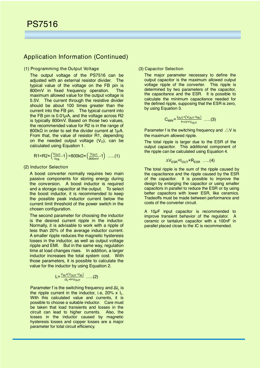
The output voltage of the PS7516 can be
The output voltage of the PS7516 can be
adjusted with an external resistor divider. The
adjusted with an external resistor divider. The
typical value of the voltage on the FB pin is
typical value of the voltage on the FB pin is
800mV in fixed frequency operation. The
800mV in fixed frequency operation. The
maximum allowed value for the output voltage is
maximum allowed value for the output voltage is
5.5V. The current through the resistive divider
5.5V. The current through the resistive divider
should be about 100 times greater than the
should be about 100 times greater than the
current into the FB pin. The typical current into
current into the FB pin. The typical current into
the FB pin is 0.01µA, and the voltage across R2
the FB pin is 0.01µA, and the voltage across R2
is typically 800mV. Based on those two values,
is typically 800mV. Based on those two values,
the recommended value for R2 is in the range of
the recommended value for R2 is in the range of
800kΩ in order to set the divider current at 1µA.
800kΩ in order to set the divider current at 1µA.
From that, the value of resistor R1, depending
From that, the value of resistor R1, depending
on the needed output voltage (VO), can be
on the needed output voltage (VO), can be
calculated using Equation 1.
calculated using Equation 1.
R1 R2 O T
R1 R2 O T
F
F
-1 800kΩ O T
-1 800kΩ O T
800m
800m
-1 …..(1)
-1 …..(1)
(2) Inductor Selection
(2) Inductor Selection
A boost converter normally requires two main
A boost converter normally requires two main
passive components for storing energy during
passive components for storing energy during
the conversion. A boost inductor is required
the conversion. A boost inductor is required
and a storage capacitor at the output. To select
and a storage capacitor at the output. To select
the boost inductor, it is recommended to keep
the boost inductor, it is recommended to keep
the possible peak inductor current below the
the possible peak inductor current below the
current limit threshold of the power switch in the
current limit threshold of the power switch in the
chosen configuration.
chosen configuration.
The second parameter for choosing the inductor
The second parameter for choosing the inductor
is the desired current ripple in the inductor.
is the desired current ripple in the inductor.
Normally, it is advisable to work with a ripple of
Normally, it is advisable to work with a ripple of
less than 20% of the average inductor current.
less than 20% of the average inductor current.
A smaller ripple reduces the magnetic hysteresis
A smaller ripple reduces the magnetic hysteresis
losses in the inductor, as well as output voltage
losses in the inductor, as well as output voltage
ripple and EMI. But in the same way, regulation
ripple and EMI. But in the same way, regulation
time at load changes rises. In addition, a larger
time at load changes rises. In addition, a larger
inductor increases the total system cost. With
inductor increases the total system cost. With
those parameters, it is possible to calculate the
those parameters, it is possible to calculate the
value for the inductor by using Equation 2.
value for the inductor by using Equation 2.
N O T- N
N O T- N
O T
O T
…..(2)
…..(2)
Parameter is the switching requency and Δ L is
Parameter is the switching requency and Δ L is
the ripple current in the inductor, i.e, 20% x IL.
the ripple current in the inductor, i.e, 20% x IL.
With this calculated value and currents, it is
With this calculated value and currents, it is
possible to choose a suitable inductor. Care must
possible to choose a suitable inductor. Care must
be taken that load transients and losses in the
be taken that load transients and losses in the
circuit can lead to higher currents. Also, the
circuit can lead to higher currents. Also, the
losses
losses
inductor caused by magnetic
inductor caused by magnetic
hysteresis losses and copper losses are a major
hysteresis losses and copper losses are a major
parameter for total circuit efficiency.
parameter for total circuit efficiency.
the
the
in
in
The major parameter necessary to define the
The major parameter necessary to define the
output capacitor is the maximum allowed output
output capacitor is the maximum allowed output
voltage ripple of the converter. This ripple is
voltage ripple of the converter. This ripple is
determined by two parameters of the capacitor,
determined by two parameters of the capacitor,
the capacitance and the ESR. It is possible to
the capacitance and the ESR. It is possible to
calculate the minimum capacitance needed for
calculate the minimum capacitance needed for
the defined ripple, supposing that the ESR is zero,
the defined ripple, supposing that the ESR is zero,
by using Equation 3.
by using Equation 3.
M N
M N
O T O T- N
O T O T- N
O T
O T
…..(3)
…..(3)
Parameter f is the switching frequency and △V is
Parameter f is the switching frequency and △V is
the maximum allowed ripple.
the maximum allowed ripple.
The total ripple is larger due to the ESR of the
The total ripple is larger due to the ESR of the
output capacitor. This additional component of
output capacitor. This additional component of
the ripple can be calculated using Equation 4.
the ripple can be calculated using Equation 4.
ESR O T RESR …..(4)
ESR O T RESR …..(4)
The total ripple is the sum of the ripple caused by
The total ripple is the sum of the ripple caused by
the capacitance and the ripple caused by the ESR
the capacitance and the ripple caused by the ESR
of the capacitor. It is possible to improve the
of the capacitor. It is possible to improve the
design by enlarging the capacitor or using smaller
design by enlarging the capacitor or using smaller
capacitors in parallel to reduce the ESR or by using
capacitors in parallel to reduce the ESR or by using
better capacitors with lower ESR, like ceramics.
better capacitors with lower ESR, like ceramics.
Tradeoffs must be made between performance and
Tradeoffs must be made between performance and
costs of the converter circuit.
costs of the converter circuit.
A 10µF input capacitor
A 10µF input capacitor
is recommended to
is recommended to
improve transient behavior of the regulator. A
improve transient behavior of the regulator. A
ceramic or tantalum capacitor with a 100nF in
ceramic or tantalum capacitor with a 100nF in
parallel placed close to the IC is recommended.
parallel placed close to the IC is recommended.
6
�
85T
85T
PS7516
PS7516
.
.
Application Information (Continued)
Application Information (Continued)
Layout Considerations
Layout Considerations
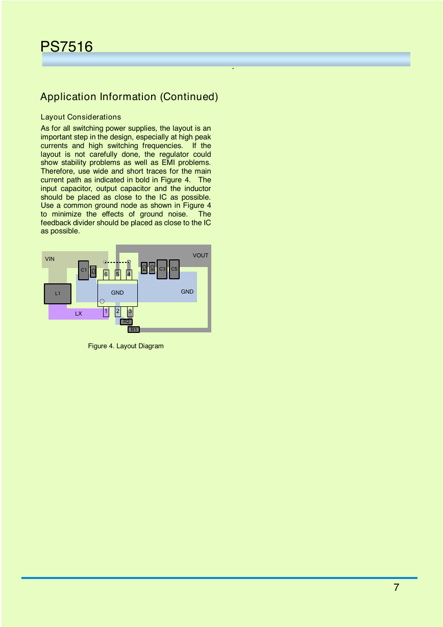
As for all switching power supplies, the layout is an
As for all switching power supplies, the layout is an
important step in the design, especially at high peak
important step in the design, especially at high peak
currents and high switching frequencies. If the
currents and high switching frequencies. If the
layout is not carefully done, the regulator could
layout is not carefully done, the regulator could
show stability problems as well as EMI problems.
show stability problems as well as EMI problems.
Therefore, use wide and short traces for the main
Therefore, use wide and short traces for the main
current path as indicated in bold in Figure 4. The
current path as indicated in bold in Figure 4. The
input capacitor, output capacitor and the inductor
input capacitor, output capacitor and the inductor
should be placed as close to the IC as possible.
should be placed as close to the IC as possible.
Use a common ground node as shown in Figure 4
Use a common ground node as shown in Figure 4
to minimize the effects of ground noise. The
to minimize the effects of ground noise. The
feedback divider should be placed as close to the IC
feedback divider should be placed as close to the IC
as possible.
as possible.
VIN
VIN
VOUT
VOUT
C1
C1
C
C
2
2
6
6
5
5
4
4
C
C
4
4
C
C
6
6
C3
C3
C5
C5
L1
L1
GND
GND
GND
GND
LX
LX
1
1
2
2
3
3
R2
R2
R1
R1
Figure 4. Layout Diagram
Figure 4. Layout Diagram
7
7
�
PS7516
PS7516
Outline Information
Outline Information
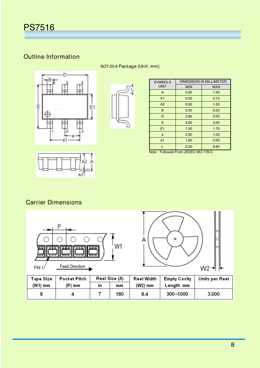
SOT-23-6 Package (Unit: mm)
SOT-23-6 Package (Unit: mm)
85T
85T
SYMBOLS
SYMBOLS
UNIT
UNIT
A
A
A1
A1
A2
A2
B
B
D
D
E
E
E1
E1
e
e
e1
e1
L
L
DIMENSION IN MILLIMETER
DIMENSION IN MILLIMETER
MIN
MIN
0.90
0.90
0.00
0.00
0.90
0.90
0.30
0.30
2.80
2.80
2.60
2.60
1.50
1.50
0.90
0.90
1.80
1.80
0.30
0.30
MAX
MAX
1.45
1.45
0.15
0.15
1.30
1.30
0.50
0.50
3.00
3.00
3.00
3.00
1.70
1.70
1.00
1.00
2.00
2.00
0.60
0.60
Note:Followed From JEDEC MO-178-C.
Note:Followed From JEDEC MO-178-C.
Carrier Dimensions
Carrier Dimensions
8
8
�


 2023年江西萍乡中考道德与法治真题及答案.doc
 2012年重庆南川中考生物真题及答案.doc
 2013年江西师范大学地理学综合及文艺理论基础考研真题.doc
 2020年四川甘孜小升初语文真题及答案I卷.doc
 2020年注册岩土工程师专业基础考试真题及答案.doc
 2023-2024学年福建省厦门市九年级上学期数学月考试题及答案.doc
 2021-2022学年辽宁省沈阳市大东区九年级上学期语文期末试题及答案.doc
 2022-2023学年北京东城区初三第一学期物理期末试卷及答案.doc
 2018上半年江西教师资格初中地理学科知识与教学能力真题及答案.doc
 2012年河北国家公务员申论考试真题及答案-省级.doc
 2020-2021学年江苏省扬州市江都区邵樊片九年级上学期数学第一次质量检测试题及答案.doc
 2022下半年黑龙江教师资格证中学综合素质真题及答案.doc