Table of Contents
Module 1: Getting Started With Altium Designer
Introduction to Altium Designer .........................................................................................1-1
1.1
The Altium Designer environment.....................................................................................1-2
1.2
1.3
Document Editor Overview................................................................................................1-6
1.4 Working with projects and documents ............................................................................1-10
Module 2: Help and DXP system menu
2.1
2.2
2.3
Using the Help system.......................................................................................................2-1
Using the Altium website ...................................................................................................2-3
DXP System menu...........................................................................................................2-10
Module 3: Schematic Editor Basics
3.1
3.2
3.3
Schematic Editor basics ....................................................................................................3-1
Schematic graphical objects..............................................................................................3-4
Schematic electrical objects ..............................................................................................3-9
Module 4: Schematic Capture
4.1
4.2
4.3
4.4
Introduction to Schematic Capture....................................................................................4-1
The Schematic Editor workspace......................................................................................4-2
Libraries and components .................................................................................................4-9
Placing and wiring............................................................................................................4-17
Module 5: Multi-Sheet Design
5.1 Multi-Sheet Design.............................................................................................................5-1
Module 6: Building the Project
6.1
6.2
Assigning designators........................................................................................................6-1
Compiling and verifying the project ...................................................................................6-5
Module 7: Setting Up for Transfer to PCB and Importing Data
7.1
Setting Up for Transfer to PCB..........................................................................................7-1
Module 8: PCB Editor Basics
8.1
PCB Editor Basics..............................................................................................................8-1
�
8.2
PCB design objects............................................................................................................8-4
Module 9: Setting up the PCB
9.1
9.2
9.3
Setting up the PCB.............................................................................................................9-1
Creating a new PCB ..........................................................................................................9-6
Setting up the PCB layers................................................................................................9-10
Module 10: Global Editing
10.1 Editing Multiple Text Objects ...........................................................................................10-1
10.2 The Data Editing System.................................................................................................10-4
Module 11: PCB Design Flow, Transferring a Design and Navigation
11.1 PCB design process ........................................................................................................11-1
11.2 Transferring design information to the PCB......................................................................11-3
11.3 Using the PCB Panel .......................................................................................................11-7
11.4 Project Navigation and Cross Probing..........................................................................11-16
Module 12: Design Rules
12.1 Design rules and design rule checking ...........................................................................12-1
Module 13: Classes and Rooms
13.1 Object classes..................................................................................................................13-1
13.2 Rooms ..............................................................................................................................13-3
Module 14: Placement and Re-annotation
14.1 Component Placement tools ...........................................................................................14-1
14.2 Re-Annotation and back annotate...................................................................................14-3
Module 15: Schematic Library Editor
15.1
Introduction to Library Editing..........................................................................................15-1
15.2 Schematic Library Editor..................................................................................................15-2
Module 16: PCB Library Editor
16.1 PCB Library Editor ...........................................................................................................16-1
16.2 3D dimensional component detail.................................................................................16-14
Module 17: Linking Models, Parameters, Library Package and Updates
17.1 Adding Model and Parameter Detail to a Component ..................................................17-1
17.2 Component Auditing ........................................................................................................17-8
17.3 3D PCB Components ....................................................................................................17-14
17.4 Library Package types ...................................................................................................17-18
17.5 Library Reports...............................................................................................................17-20
�
Module 18: Routing and Polygons
18.1 Routing .............................................................................................................................18-1
18.2 Testpoint System ...........................................................................................................18-10
18.3 Adding and removing teardrops ....................................................................................18-15
18.4 Automatic routing ...........................................................................................................18-16
18.5 Polygons and the Polygon Manager.............................................................................18-19
Module 19: Output Generation and CAM File Editing
19.1 Bill of Materials .................................................................................................................19-1
19.2 Output Generation............................................................................................................19-8
19.3 CAM Editor .....................................................................................................................19-20
Module 20: Interfacing to 3D Mechanical CAD
20.1
Interfacing to 3D Mechanical CAD..................................................................................20-1
�
Module 1: Getting Started
With Altium Designer
�
Module 1: Getting Started With Altium Designer
1.1
Introduction to Altium Designer...................................................... 1-1
1.1.1 The Altium Designer Integration Platform ......................................................1-1
1.2 The Altium Designer environment .................................................. 1-2
1.2.1 The Altium Designer Project ..........................................................................1-3
1.2.2 Demo — Opening an existing Project............................................................1-3
1.2.3 Editor View .....................................................................................................1-4
1.2.4 Exercises — Navigating around Altium Designer ..........................................1-5
1.3 Document Editor Overview.............................................................. 1-6
1.3.1 Working in a document editor ........................................................................1-6
1.4 Working with projects and documents......................................... 1-10
1.4.1 Creating a new project .................................................................................1-10
1.4.2 Adding a new document to the project.........................................................1-11
1.4.3 Adding an existing document to a project ...................................................1-11
1.4.4 Moving or copying a document between projects........................................1-11
1.4.5 Removing a document from the project .......................................................1-11
1.4.6 File management with the Storage Manager ...............................................1-12
1.4.7
Including other files in the Altium Designer project ......................................1-12
1.4.8 Libraries........................................................................................................1-13
1.4.9 Project Packager..........................................................................................1-13
1.4.10 Exercise – Working with projects and documents .......................................1-14
Software, documentation and related materials:
Copyright © 2009 Altium Limited.
All rights reserved. You are permitted to print this document provided that (1) the use of such is for personal use only and will
not be copied or posted on any network computer or broadcast in any media, and (2) no modifications of the document is
made. Unauthorized duplication, in whole or part, of this document by any means, mechanical or electronic, including
translation into another language, except for brief excerpts in published reviews, is prohibited without the express written
permission of Altium Limited. Unauthorized duplication of this work may also be prohibited by local statute. Violators may be
subject to both criminal and civil penalties, including fines and/or imprisonment. Altium, Altium Designer, Board Insight, Design
Explorer, DXP, LiveDesign, NanoBoard, NanoTalk, P-CAD, SimCode, Situs, TASKING, and Topological Autorouting and their
respective logos are trademarks or registered trademarks of Altium Limited or its subsidiaries. All other registered or
unregistered trademarks referenced herein are the property of their respective owners and no trademark rights to the same are
claimed.
Module Seq = 1
�
1.1
Introduction to Altium Designer
Underlying the Altium Designer environment is a software integration platform that brings
together all the tools necessary to create a complete environment for electronic product
development, in a single application.
Altium Designer includes tools for all design tasks: from schematic and HDL design capture,
circuit simulation, signal integrity analysis, PCB design, and FPGA-based embedded system
design and development. In addition, the Altium Designer environment can be customized to
meet a wide variety of user requirements.
1.1.1 The Altium Designer Integration Platform
When you select All Programs » Altium Designer Summer 09 from the Windows Start menu
to run Altium Designer, you are actually launching DXP.EXE. The DXP platform underlies Altium
Designer, supporting each of the editors that you use to create your design.
The application interface is automatically configured to suit the document you are working on.
For example, if you open a schematic sheet, appropriate toolbars, menus and shortcut keys are
activated. This feature means that you can switch from routing a PCB, to producing a Bill of
Materials report, to running a transient circuit analysis, and so on – and the correct menus,
toolbars and shortcuts will be readily available.
Also, all toolbars, menus and shortcut keys can also be configured to suit how you like to
configure your design environment.
Figure 1. Altium Designer’s software integration architecture
Module 1: Getting started With Altium Designer
1 - 1
�
1.2 The Altium Designer environment
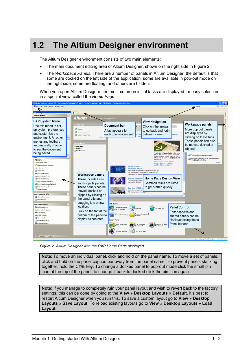
The Altium Designer environment consists of two main elements:
• The main document editing area of Altium Designer, shown on the right side in
• The Workspace Panels. There are a number of panels in Altium Designer, the default is that
some are docked on the left side of the application, some are available in pop-out mode on
the right side, some are floating, and others are hidden.
Figure 2
.
When you open Altium Designer, the most common initial tasks are displayed for easy selection
in a special view, called the Home Page.
s
DXP System Menu
Use this menu to set
up system preference
and customize the
environment. All other
menus and toolbars
automatically change
to suit the documen
t
being edited.
Document bar
A tab appears for
each open document.
View Navigation
Click on the arrows
to go back and forth
between views.
Workspace panels
More pop out panels
are displayed by
clicking on these tabs.
These panels can also
be moved, docked or
clipped.
Workspace panels
These include Files
and Projects panels.
These panels can be
moved, docked or
clipped by clicking on
the panel title and
dragging it to a new
location.
Click on the tab at the
bottom of the panel to
display its contents.
Home Page Design View
Common tasks are listed
to get started quickly.
Panel Control
Editor specific and
shared panels can be
displayed using these
Panel buttons.
Figure 2. Altium Designer with the DXP Home Page displayed.
Note: To move an individual panel, click and hold on the panel name. To move a set of panels,
click and hold on the panel caption bar away from the panel name. To prevent panels stacking
together, hold the CTRL key. To change a docked panel to pop-out mode click the small pin
icon at the top of the panel, to change it back to docked click the pin icon again.
Note: If you manage to completely ruin your panel layout and wish to revert back to the factory
settings, this can be done by going to the View » Desktop Layouts » Default. It’s best to
restart Altium Designer when you run this. To save a custom layout go to View » Desktop
Layouts » Save Layout. To reload existing layouts go to View » Desktop Layouts » Load
Layout.
Module 1: Getting started With Altium Designer
1 - 2
�
1.2.1 The Altium Designer Project
• The basis of every electronic product design is the project.
• The project links the elements of your design together, including the source schematics, the
PCB, the netlist, and any libraries or models you want to keep in the project.
• The project also stores the project-level options, such as the error checking settings, the
multi-sheet connectivity mode, and the multi-channel annotation scheme.
• There are six project types – PCB projects, FPGA projects, Core Projects, Embedded
Projects, Script Projects and Library Packages (the source for an integrated library).
• Altium Designer allows you to access all documents related to a project via the Projects
panel.
• Related projects can also be linked under a common Workspace, giving easy access to all
files related to a particular product your company is developing.
• When you add documents to a project, such as a schematic sheet, a link to each document
is entered into the project file. The documents can be stored anywhere on your network; they
do not need to be in the same folder as the project file. If they do exist in a directory outside
where the project exists or its sub-directories, then a small arrow symbol appears on the
document’s icon in the Projects panel.
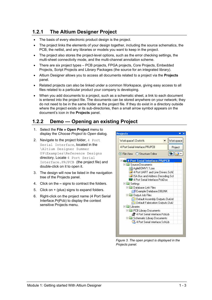
1.2.2 Demo — Opening an existing Project
1. Select the File » Open Project menu to
display the Choose Project to Open dialog.
2. Navigate to the project folder, 4 Port
Serial Interface, located in the
\Altium Designer Summer
09\Examples\Reference Designs
directory. Locate 4 Port Serial
Interface.PRJPCB (the project file) and
double-click on it to open it.
3. The design will now be listed in the navigation
tree of the Projects panel.
4. Click on the – signs to contract the folders.
5. Click on + (plus) signs to expand folders.
6. Right-click on the project name (4 Port Serial
Interface.PrjPcb) to display the context
sensitive Projects menu.
Figure 3. The open project is displayed in the
Projects panel.
Module 1: Getting started With Altium Designer
1 - 3
�





 2023年江西萍乡中考道德与法治真题及答案.doc
 2012年重庆南川中考生物真题及答案.doc
 2013年江西师范大学地理学综合及文艺理论基础考研真题.doc
 2020年四川甘孜小升初语文真题及答案I卷.doc
 2020年注册岩土工程师专业基础考试真题及答案.doc
 2023-2024学年福建省厦门市九年级上学期数学月考试题及答案.doc
 2021-2022学年辽宁省沈阳市大东区九年级上学期语文期末试题及答案.doc
 2022-2023学年北京东城区初三第一学期物理期末试卷及答案.doc
 2018上半年江西教师资格初中地理学科知识与教学能力真题及答案.doc
 2012年河北国家公务员申论考试真题及答案-省级.doc
 2020-2021学年江苏省扬州市江都区邵樊片九年级上学期数学第一次质量检测试题及答案.doc
 2022下半年黑龙江教师资格证中学综合素质真题及答案.doc