Omni
ision ®
General Description
The OV7725 CAMERACHIP™ image sensor is a low
voltage CMOS device that provides the full functionality of
a single-chip VGA camera and image processor in a small
footprint package. The OV7725 provides full-frame,
sub-sampled or windowed 8-bit/10-bit images in a wide
range of formats, controlled through the Serial Camera
Control Bus (SCCB) interface.
This device has an image array capable of operating at up
to 60 frames per second (fps) in VGA with complete user
control over image quality, formatting and output data
transfer. All
functions,
including exposure control, gamma, white balance, color
saturation, hue control and more, are also programmable
through the SCCB interface. In addition, OmniVision
sensors use proprietary sensor technology to improve
image quality by reducing or eliminating common
lighting/electrical sources of image contamination, such
as fixed pattern noise, smearing, blooming, etc., to
produce a clean, fully stable color image.
image processing
required
Pb
Note: The OV7725 uses a lead-free
package.
Features
High sensitivity for low-light operation
Standard SCCB interface
•
•
• Output support for Raw RGB, RGB (GRB 4:2:2,
RGB565/555/444) and YCbCr (4:2:2) formats
Supports image sizes: VGA, QVGA, and any size
scaling down from CIF to 40x30
VarioPixel® method for sub-sampling
Automatic image control functions including:
Automatic Exposure Control (AEC), Automatic Gain
Control (AGC), Automatic White Balance (AWB),
Automatic Band Filter (ABF), and Automatic
Black-Level Calibration (ABLC)
Image quality controls including color saturation,
hue, gamma, sharpness (edge enhancement), and
anti-blooming
ISP includes noise reduction and defect correction
Lens shading correction
Saturation level auto adjust (UV adjust)
Edge enhancement level auto adjust
De-noise level auto adjust
Frame synchronization capability
•
•
•
•
•
•
•
•
•
•
Ordering Information
Product
Package
OV07725-VL1A (Color, lead-free)
28-pin CSP2
Advanced Information
Datasheet
OV7725 Color CMOS VGA (640x480) CAMERACHIPTM Sensor
with OmniPixel2TM Technology
Applications
•
•
•
•
Cellular and picture phones
Toys
PC Multimedia
Digital still cameras
Key Specifications
Power Supply
Power
Requirements
Array Size 640 x 480
Digital Core 1.8VDC + 10%
Analog 3.0V to 3.6V
I/O 1.7V to 3.3V
Active 120 mW typical
Standby < 20 µA
(60 fps VGA, YUV)
Temperature Range -20°C to +70°C
Output Format
8-bit
• YUV/YCbCr 4:2:2
• RGB565/555/444
• GRB 4:2:2
• Raw RGB Data
• Raw RGB Data
10-bit
Lens Size 1/4"
Lens Chief Ray Angle 25° non linear
Max Image Transfer Rate 60 fps for VGA
Sensitivity 3.8 V/(Lux • sec)
S/N Ratio 50 dB
Dynamic Range 60 dB
Scan Mode Progressive
Electronic Exposure Up to 510:1 (for selected fps)
Pixel Size 6.0 µm x 6.0 µm
Dark Current 40 mV/s
Well Capacity 26 Ke-
Fixed Pattern Noise < 0.03% of VPEAK-TO-PEAK
Image Area 3984 µm x 2952 µm
Package Dimensions 5345 µm x 5265 µm
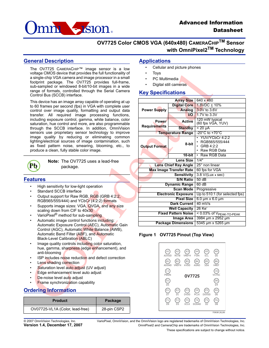
Figure 1 OV7725 Pinout (Top View)
A1
ADVDD
A2
RSTB
A3
VREFH
A4
FSIN
B1
B2
B3
B4
ADGND
VREFN
AVDD
AGND
A5
SCL
B5
SDA
C1
PWDN
D1
D5
E1
D7
F1
D9
OV7725
E2
D1
F2
D3
E3
DVDD
E4
PCLK
E5
DOVDD
F3
F4
XCLK
DOGND
F5
D2
A6
D0
B6
HREF
C6
VSYNC
D6
D4
E6
D6
F6
D8
7725CSP_DS_001
© 2007 OmniVision Technologies, Inc.
Version 1.4, December 17, 2007
VarioPixel, OmniVision, and the OmniVision logo are registered trademarks of OmniVision Technologies, Inc.
OmniPixel2 and CameraChip are trademarks of OmniVision Technologies, Inc.
These specifications are subject to change without notice.
�
OV7725
Color CMOS VGA OmniPixel2™ CAMERACHIP™ Sensor
Omni
ision
Functional Description
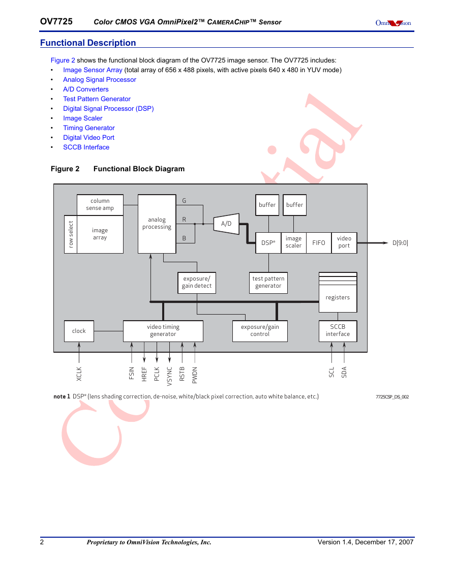
Figure 2 shows the functional block diagram of the OV7725 image sensor. The OV7725 includes:
•
•
•
•
•
•
•
•
•
Image Sensor Array (total array of 656 x 488 pixels, with active pixels 640 x 480 in YUV mode)
Analog Signal Processor
A/D Converters
Test Pattern Generator
Digital Signal Processor (DSP)
Image Scaler
Timing Generator
Digital Video Port
SCCB Interface
Figure 2 Functional Block Diagram
column
sense amp
image
array
t
c
e
l
e
s
w
o
r
analog
processing
G
R
B
buffer
buffer
A/D
DSP*
image
scaler
FIFO
video
port
D[9:0]
exposure/
gain detect
test pattern
generator
video timing
generator
exposure/gain
control
I
N
S
F
F
E
R
H
K
L
C
P
C
N
Y
S
V
B
T
S
R
N
D
W
P
registers
SCCB
interface
L
C
S
A
D
S
clock
K
L
C
X
note 1
DSP* (lens shading correction, de-noise, white/black pixel correction, auto white balance, etc.)
7725CSP_DS_002
2
Proprietary to OmniVision Technologies, Inc.
Version 1.4, December 17, 2007
�
Omni
ision
Image Sensor Array
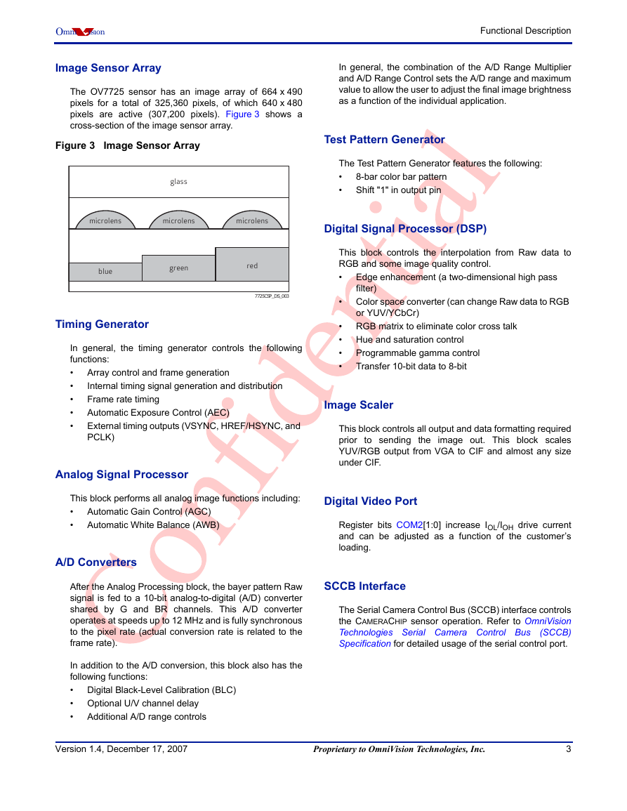
The OV7725 sensor has an image array of 664 x 490
pixels for a total of 325,360 pixels, of which 640 x 480
pixels are active (307,200 pixels). Figure 3 shows a
cross-section of the image sensor array.
Figure 3 Image Sensor Array
glass
Functional Description
In general, the combination of the A/D Range Multiplier
and A/D Range Control sets the A/D range and maximum
value to allow the user to adjust the final image brightness
as a function of the individual application.
Test Pattern Generator
The Test Pattern Generator features the following:
•
•
8-bar color bar pattern
Shift "1" in output pin
microlens
microlens
microlens
Digital Signal Processor (DSP)
blue
green
red
7725CSP_DS_003
Timing Generator
In general, the timing generator controls the following
functions:
•
•
•
•
•
Array control and frame generation
Internal timing signal generation and distribution
Frame rate timing
Automatic Exposure Control (AEC)
External timing outputs (VSYNC, HREF/HSYNC, and
PCLK)
Analog Signal Processor
This block performs all analog image functions including:
•
•
Automatic Gain Control (AGC)
Automatic White Balance (AWB)
A/D Converters
This block controls the interpolation from Raw data to
RGB and some image quality control.
•
Edge enhancement (a two-dimensional high pass
filter)
Color space converter (can change Raw data to RGB
or YUV/YCbCr)
RGB matrix to eliminate color cross talk
Hue and saturation control
Programmable gamma control
Transfer 10-bit data to 8-bit
•
•
•
•
•
Image Scaler
This block controls all output and data formatting required
prior to sending the image out. This block scales
YUV/RGB output from VGA to CIF and almost any size
under CIF.
Digital Video Port
Register bits COM2[1:0] increase IOL/IOH drive current
and can be adjusted as a function of the customer’s
loading.
After the Analog Processing block, the bayer pattern Raw
signal is fed to a 10-bit analog-to-digital (A/D) converter
shared by G and BR channels. This A/D converter
operates at speeds up to 12 MHz and is fully synchronous
to the pixel rate (actual conversion rate is related to the
frame rate).
SCCB Interface
The Serial Camera Control Bus (SCCB) interface controls
the CAMERACHIP sensor operation. Refer to OmniVision
Technologies Serial Camera Control Bus
(SCCB)
Specification for detailed usage of the serial control port.
In addition to the A/D conversion, this block also has the
following functions:
•
• Optional U/V channel delay
•
Digital Black-Level Calibration (BLC)
Additional A/D range controls
Version 1.4, December 17, 2007
Proprietary to OmniVision Technologies, Inc.
3
�
OV7725
Color CMOS VGA OmniPixel2™ CAMERACHIP™ Sensor
Omni
ision
Pin Description
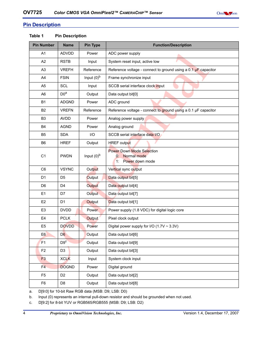
Table 1
Pin Description
Pin Number
Name
Pin Type
Function/Description
A1
A2
A3
A4
A5
A6
B1
B2
B3
B4
B5
B6
C1
C6
D1
D6
E1
E2
E3
E4
E5
E6
F1
F2
F3
F4
F5
F6
ADVDD
RSTB
VREFH
FSIN
SCL
D0a
ADGND
VREFN
AVDD
AGND
SDA
HREF
Power
Input
Reference
Input (0)b
Input
Output
Power
ADC power supply
System reset input, active low
Reference voltage - connect to ground using a 0.1 µF capacitor
Frame synchronize input
SCCB serial interface clock input
Data output bit[0]
ADC ground
Reference
Reference voltage - connect to ground using a 0.1 µF capacitor
Power
Power
I/O
Analog power supply
Analog ground
SCCB serial interface data I/O
Output
HREF output
PWDN
Input (0)b
Power Down Mode Selection
0: Normal mode
1: Power down mode
VSYNC
D5
D4
D7
D1
DVDD
PCLK
DOVDD
D6
D9c
D3
XCLK
DOGND
D2
D8
Output
Output
Output
Output
Output
Power
Output
Power
Output
Output
Output
Input
Power
Output
Output
Vertical sync output
Data output bit[5]
Data output bit[4]
Data output bit[7]
Data output bit[1]
Power supply (1.8 VDC) for digital logic core
Pixel clock output
Digital power supply for I/O (1.7V ~ 3.3V)
Data output bit[6]
Data output bit[9]
Data output bit[3]
System clock input
Digital ground
Data output bit[2]
Data output bit[8]
a. D[9:0] for 10-bit Raw RGB data (MSB: D9; LSB: D0)
b.
c. D[9:2] for 8-bit YUV or RGB565/RGB555 (MSB: D9; LSB: D2)
Input (0) represents an internal pull-down resistor and should be grounded when not used.
4
Proprietary to OmniVision Technologies, Inc.
Version 1.4, December 17, 2007
�
Omni
ision
Electrical Characteristics
Electrical Characteristics
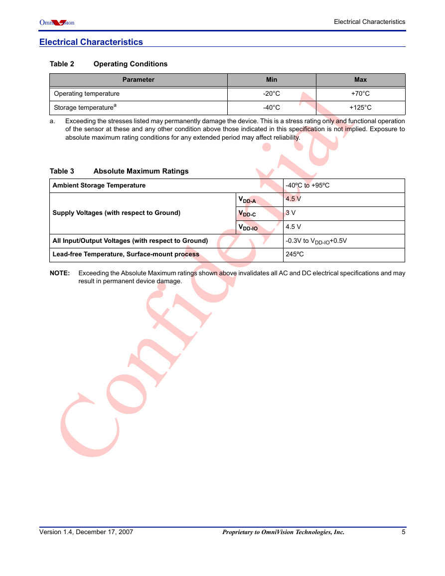
Table 2
Operating Conditions
Parameter
Operating temperature
Storage temperaturea
Min
-20°C
-40°C
Max
+70°C
+125°C
a. Exceeding the stresses listed may permanently damage the device. This is a stress rating only and functional operation
of the sensor at these and any other condition above those indicated in this specification is not implied. Exposure to
absolute maximum rating conditions for any extended period may affect reliability.
Table 3
Ambient Storage Temperature
Absolute Maximum Ratings
Supply Voltages (with respect to Ground)
-40ºC to +95ºC
VDD-A
VDD-C
VDD-IO
4.5 V
3 V
4.5 V
All Input/Output Voltages (with respect to Ground)
Lead-free Temperature, Surface-mount process
-0.3V to VDD-IO+0.5V
245ºC
NOTE: Exceeding the Absolute Maximum ratings shown above invalidates all AC and DC electrical specifications and may
result in permanent device damage.
Version 1.4, December 17, 2007
Proprietary to OmniVision Technologies, Inc.
5
�
OV7725
Color CMOS VGA OmniPixel2™ CAMERACHIP™ Sensor
Omni
ision
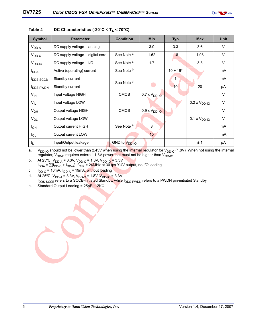
Table 4
DC Characteristics (-20°C < TA < 70°C)
Symbol
Parameter
Condition
Min
Typ
Max
Unit
–
10 + 19c
3.3
1.8
–
1
10
3.6
1.98
3.3
3.0
1.62
1.7
Standby current
Input voltage HIGH
DC supply voltage – I/O
Active (operating) current
DC supply voltage – analog
DC supply voltage – digital core
See Note a
See Note a
See Note b
VDD-A
VDD-C
VDD-IO
IDDA
IDDS-SCCB
IDDS-PWDN Standby current
VIH
VIL
VOH
VOL
IOH
IOL
IL
a. VDD-IO should not be lower than 2.45V when using the internal regulator for VDD-C (1.8V). When not using the internal
Input/Output leakage
Output voltage HIGH
Output current HIGH
Output voltage LOW
Output current LOW
Input voltage LOW
GND to VDD-IO
mA
mA
µA
mA
mA
µA
0.2 x VDD-IO
0.1 x VDD-IO
0.7 x VDD-IO
V
V
V
V
V
V
V
CMOS
0.9 x VDD-IO
See Note d
CMOS
20
± 1
See Note e
8
15
regulator, VDD-C requires external 1.8V power that must not be higher than VDD-IO.
b. At 25ºC, VDD-A = 3.3V, VDD-C = 1.8V, VDD-IO = 3.3V
IDDA = ∑{IDD-C + IDD-A}, fCLK = 24MHz at 30 fps YUV output, no I/O loading
IDD-C = 10mA, IDD-A = 19mA, without loading
c.
d. At 25ºC, VDD-A = 3.3V, VDD-C = 1.8V, VDD-IO = 3.3V
IDDS-SCCB refers to a SCCB-initiated Standby, while IDDS-PWDN refers to a PWDN pin-initiated Standby
e. Standard Output Loading = 25pF, 1.2KΩ
6
Proprietary to OmniVision Technologies, Inc.
Version 1.4, December 17, 2007
�
Omni
ision
Electrical Characteristics
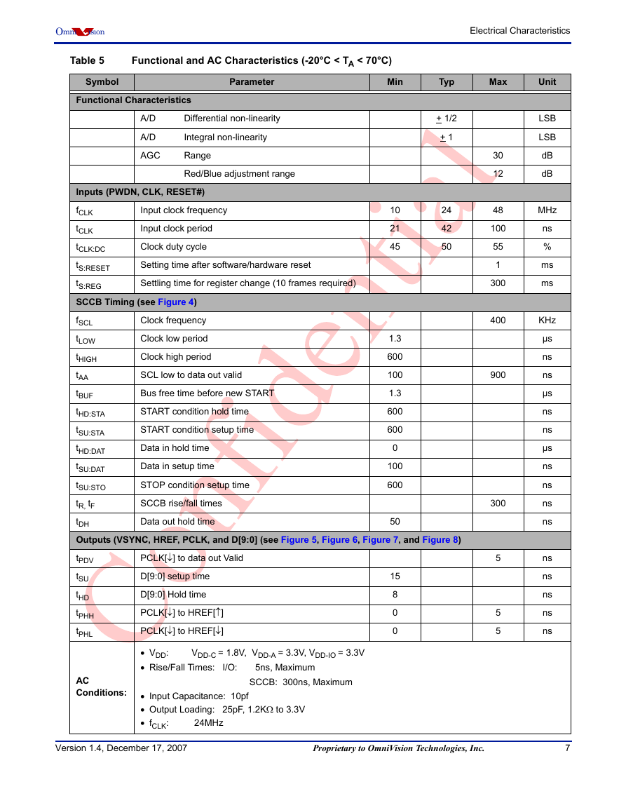
Table 5
Functional and AC Characteristics (-20°C < TA < 70°C)
Symbol
Parameter
Min
Typ
Max
Unit
Functional Characteristics
A/D
A/D
AGC
Differential non-linearity
Integral non-linearity
Range
Red/Blue adjustment range
+ 1/2
+ 1
24
42
50
Input clock frequency
Input clock period
Clock duty cycle
Setting time after software/hardware reset
Settling time for register change (10 frames required)
Inputs (PWDN, CLK, RESET#)
fCLK
tCLK
tCLK:DC
tS:RESET
tS:REG
SCCB Timing (see Figure 4)
fSCL
tLOW
tHIGH
tAA
tBUF
tHD:STA
tSU:STA
tHD:DAT
tSU:DAT
tSU:STO
tR, tF
tDH
Outputs (VSYNC, HREF, PCLK, and D[9:0] (see Figure 5, Figure 6, Figure 7, and Figure 8)
tPDV
tSU
tHD
tPHH
tPHL
Clock frequency
Clock low period
Clock high period
SCL low to data out valid
Bus free time before new START
START condition hold time
START condition setup time
Data in hold time
Data in setup time
STOP condition setup time
SCCB rise/fall times
Data out hold time
PCLK[↓] to data out Valid
D[9:0] setup time
D[9:0] Hold time
PCLK[↓] to HREF[↑]
PCLK[↓] to HREF[↓]
10
21
45
1.3
600
100
1.3
600
600
0
100
600
50
15
8
0
0
LSB
LSB
dB
dB
MHz
ns
%
ms
ms
KHz
µs
ns
ns
µs
ns
ns
µs
ns
ns
ns
ns
ns
ns
ns
ns
ns
30
12
48
100
55
1
300
400
900
300
5
5
5
AC
Conditions:
• VDD: VDD-C = 1.8V, VDD-A = 3.3V, VDD-IO = 3.3V
• Rise/Fall Times: I/O: 5ns, Maximum
SCCB: 300ns, Maximum
• Input Capacitance: 10pf
• Output Loading: 25pF, 1.2KΩ to 3.3V
• fCLK: 24MHz
Version 1.4, December 17, 2007
Proprietary to OmniVision Technologies, Inc.
7
�
OV7725
Color CMOS VGA OmniPixel2™ CAMERACHIP™ Sensor
Omni
ision
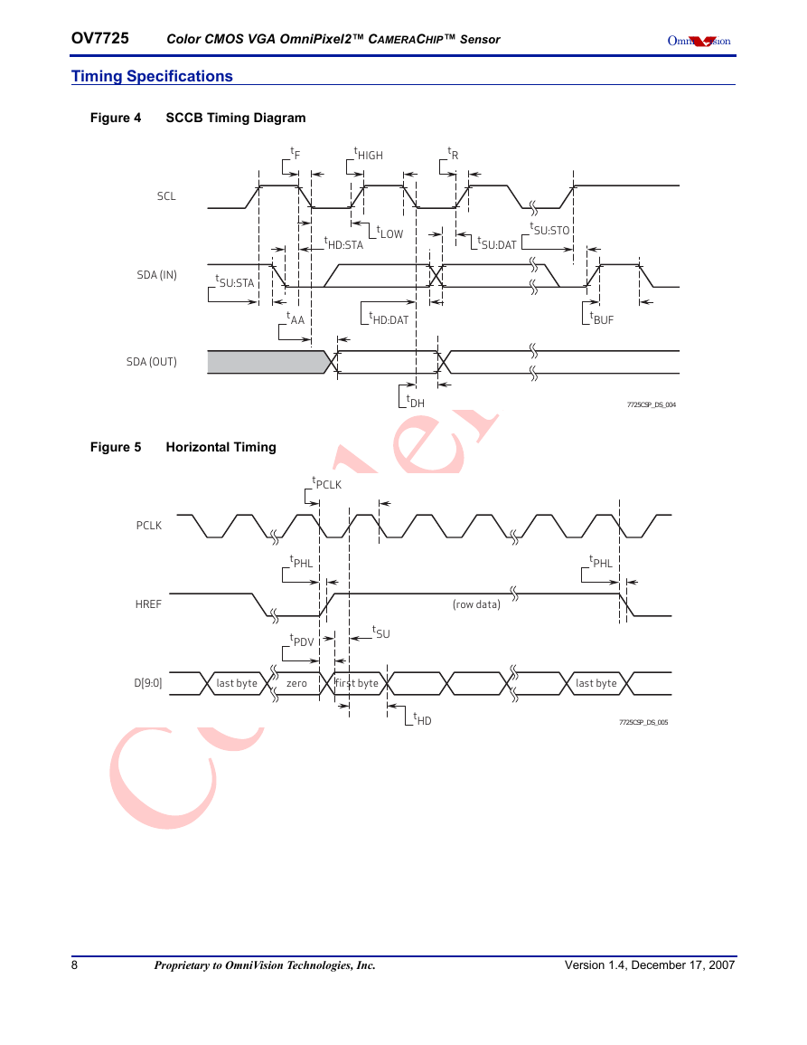
Timing Specifications
Figure 4 SCCB Timing Diagram
tF
tHIGH
tR
SCL
SDA (IN)
tSU:STA
SDA (OUT)
Figure 5 Horizontal Timing
tLOW
tHD:STA
tSU:STO
tSU:DAT
tAA
tHD:DAT
tBUF
tDH
7725CSP_DS_004
PCLK
HREF
tPCLK
tPHL
tPDV
tPHL
(row data)
tSU
D[9:0]
last byte
zero
first byte
last byte
tHD
7725CSP_DS_005
8
Proprietary to OmniVision Technologies, Inc.
Version 1.4, December 17, 2007
�


 2023年江西萍乡中考道德与法治真题及答案.doc
 2012年重庆南川中考生物真题及答案.doc
 2013年江西师范大学地理学综合及文艺理论基础考研真题.doc
 2020年四川甘孜小升初语文真题及答案I卷.doc
 2020年注册岩土工程师专业基础考试真题及答案.doc
 2023-2024学年福建省厦门市九年级上学期数学月考试题及答案.doc
 2021-2022学年辽宁省沈阳市大东区九年级上学期语文期末试题及答案.doc
 2022-2023学年北京东城区初三第一学期物理期末试卷及答案.doc
 2018上半年江西教师资格初中地理学科知识与教学能力真题及答案.doc
 2012年河北国家公务员申论考试真题及答案-省级.doc
 2020-2021学年江苏省扬州市江都区邵樊片九年级上学期数学第一次质量检测试题及答案.doc
 2022下半年黑龙江教师资格证中学综合素质真题及答案.doc