D
E
S
O
P
O
R
P
Item #JC-45-2065.01b
DDR3 SPD 0.0
DDR3 SPD 0.0
Item JC-45-2065.01b
Background:
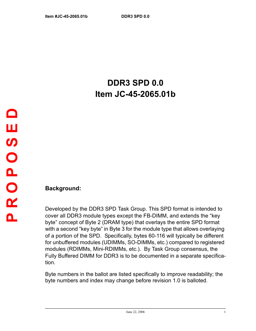
Developed by the DDR3 SPD Task Group. This SPD format is intended to
cover all DDR3 module types except the FB-DIMM, and extends the “key
byte” concept of Byte 2 (DRAM type) that overlays the entire SPD format
with a second “key byte” in Byte 3 for the module type that allows overlaying
of a portion of the SPD. Specifically, bytes 60-116 will typically be different
for unbuffered modules (UDIMMs, SO-DIMMs, etc.) compared to registered
modules (RDIMMs, Mini-RDIMMs, etc.). By Task Group consensus, the
Fully Buffered DIMM for DDR3 is to be documented in a separate specifica-
tion.
Byte numbers in the ballot are listed specifically to improve readability; the
byte numbers and index may change before revision 1.0 is balloted.
June 22, 2006
1
�
D
E
S
O
P
O
R
P
Item #JC-45-2065.01b
DDR3 SPD 0.0
Appendix X: Serial Presence Detect (SPD) for DDR3 SDRAM Modules
(Revision 0.0)
1.0 Introduction
This appendix describes the serial presence detect (SPD) values for all DDR3 modules. Differ-
ences between module types are encapsulated in subsections of this appendix. These presence
detect values are those referenced in the SPD standard document for ‘Specific Features’. The fol-
lowing SPD fields will be documented in the order presented in section 1.1 with the exception of
bytes 60-116 which are documented in separate appendices, one for each family of module types.
Further description of Byte 2 is found in Appendix A of the SPD standard. All unused entries wiil be
coded as 00h. All unused bits in defined bytes will be coded as 0 except where noted.
To allow for maximum flexibility as devices evolve, SPD fields described in this document may
support device configuration and timing options that are not included in the JEDEC DDR3 SDRAM
data sheet (JESD79-3). Please refer to DRAM supplier data sheets or JESD79-3 to determine the
compatibility of components.
1.1 Address map
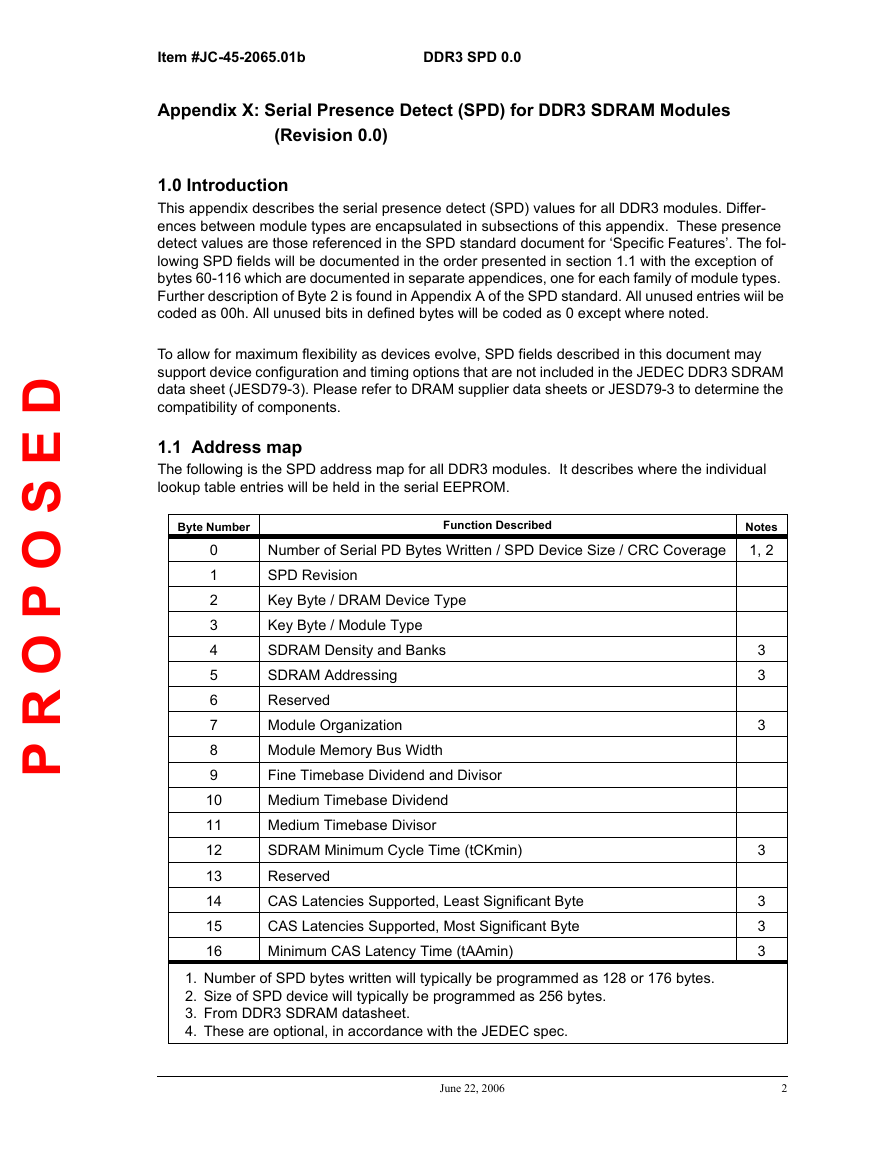
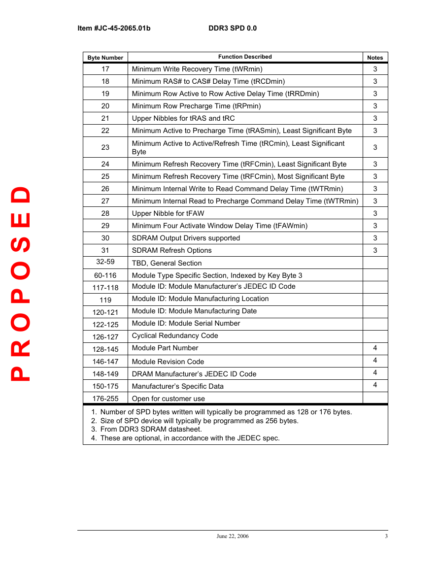
The following is the SPD address map for all DDR3 modules. It describes where the individual
lookup table entries will be held in the serial EEPROM.
Byte Number
Function Described
0
1
2
3
4
5
6
7
8
9
10
11
12
13
14
15
16
Number of Serial PD Bytes Written / SPD Device Size / CRC Coverage
SPD Revision
Key Byte / DRAM Device Type
Key Byte / Module Type
SDRAM Density and Banks
SDRAM Addressing
Reserved
Module Organization
Module Memory Bus Width
Fine Timebase Dividend and Divisor
Medium Timebase Dividend
Medium Timebase Divisor
SDRAM Minimum Cycle Time (tCKmin)
Reserved
CAS Latencies Supported, Least Significant Byte
CAS Latencies Supported, Most Significant Byte
Minimum CAS Latency Time (tAAmin)
1. Number of SPD bytes written will typically be programmed as 128 or 176 bytes.
2. Size of SPD device will typically be programmed as 256 bytes.
3. From DDR3 SDRAM datasheet.
4. These are optional, in accordance with the JEDEC spec.
Notes
1, 2
3
3
3
3
3
3
3
June 22, 2006
2
�
D
E
S
O
P
O
R
P
Item #JC-45-2065.01b
DDR3 SPD 0.0
Byte Number
Function Described
Notes
17
18
19
20
21
22
23
24
25
26
27
28
29
30
31
32-59
60-116
117-118
119
Minimum Write Recovery Time (tWRmin)
Minimum RAS# to CAS# Delay Time (tRCDmin)
Minimum Row Active to Row Active Delay Time (tRRDmin)
Minimum Row Precharge Time (tRPmin)
Upper Nibbles for tRAS and tRC
Minimum Active to Precharge Time (tRASmin), Least Significant Byte
Minimum Active to Active/Refresh Time (tRCmin), Least Significant
Byte
Minimum Refresh Recovery Time (tRFCmin), Least Significant Byte
Minimum Refresh Recovery Time (tRFCmin), Most Significant Byte
Minimum Internal Write to Read Command Delay Time (tWTRmin)
Minimum Internal Read to Precharge Command Delay Time (tWTRmin)
Upper Nibble for tFAW
Minimum Four Activate Window Delay Time (tFAWmin)
SDRAM Output Drivers supported
SDRAM Refresh Options
TBD, General Section
Module Type Specific Section, Indexed by Key Byte 3
Module ID: Module Manufacturer’s JEDEC ID Code
Module ID: Module Manufacturing Location
Module ID: Module Manufacturing Date
Module ID: Module Serial Number
Cyclical Redundancy Code
Module Part Number
Module Revision Code
DRAM Manufacturer’s JEDEC ID Code
Manufacturer’s Specific Data
Open for customer use
120-121
122-125
126-127
128-145
146-147
148-149
150-175
176-255
1. Number of SPD bytes written will typically be programmed as 128 or 176 bytes.
2. Size of SPD device will typically be programmed as 256 bytes.
3. From DDR3 SDRAM datasheet.
4. These are optional, in accordance with the JEDEC spec.
3
3
3
3
3
3
3
3
3
3
3
3
3
3
3
4
4
4
4
June 22, 2006
3
�
D
E
S
O
P
O
R
P
Item #JC-45-2065.01b
DDR3 SPD 0.0
2.0 Details of each byte
2.1 General Section: Bytes 0 to 59
This section contains defines bytes that are common to all DDR3 module types.
Byte 0: Number of Bytes Used / Number of Bytes in SPD Device / CRC
Coverage
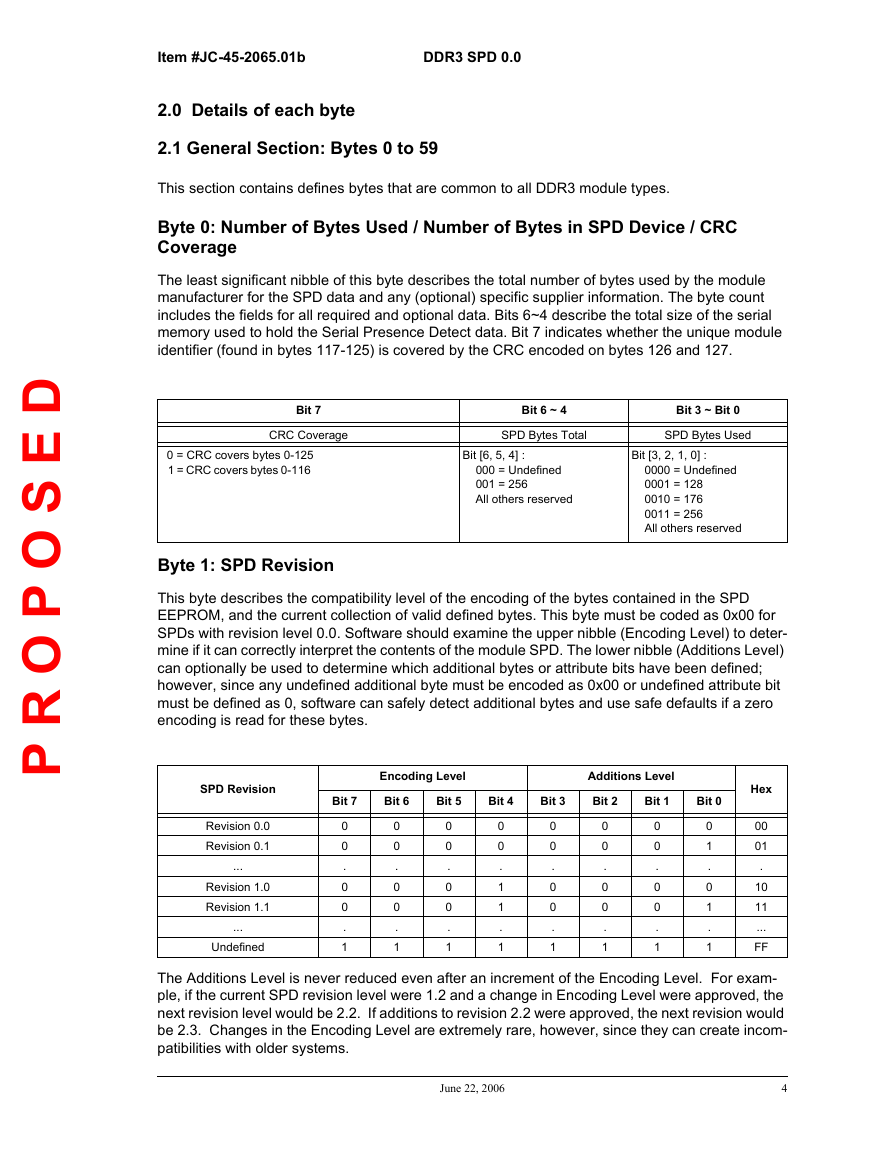
The least significant nibble of this byte describes the total number of bytes used by the module
manufacturer for the SPD data and any (optional) specific supplier information. The byte count
includes the fields for all required and optional data. Bits 6~4 describe the total size of the serial
memory used to hold the Serial Presence Detect data. Bit 7 indicates whether the unique module
identifier (found in bytes 117-125) is covered by the CRC encoded on bytes 126 and 127.
Bit 7
CRC Coverage
0 = CRC covers bytes 0-125
1 = CRC covers bytes 0-116
Bit 6 ~ 4
SPD Bytes Total
Bit [6, 5, 4] :
000 = Undefined
001 = 256
All others reserved
Bit 3 ~ Bit 0
SPD Bytes Used
Bit [3, 2, 1, 0] :
0000 = Undefined
0001 = 128
0010 = 176
0011 = 256
All others reserved
Byte 1: SPD Revision
This byte describes the compatibility level of the encoding of the bytes contained in the SPD
EEPROM, and the current collection of valid defined bytes. This byte must be coded as 0x00 for
SPDs with revision level 0.0. Software should examine the upper nibble (Encoding Level) to deter-
mine if it can correctly interpret the contents of the module SPD. The lower nibble (Additions Level)
can optionally be used to determine which additional bytes or attribute bits have been defined;
however, since any undefined additional byte must be encoded as 0x00 or undefined attribute bit
must be defined as 0, software can safely detect additional bytes and use safe defaults if a zero
encoding is read for these bytes.
SPD Revision
Revision 0.0
Revision 0.1
...
Revision 1.0
Revision 1.1
...
Undefined
Encoding Level
Additions Level
Bit 7
Bit 6
Bit 5
Bit 4
Bit 3
Bit 2
Bit 1
Bit 0
0
0
.
0
0
.
1
0
0
.
0
0
.
1
0
0
.
0
0
.
1
0
0
.
1
1
.
1
0
0
.
0
0
.
1
0
0
.
0
0
.
1
0
0
.
0
0
.
1
0
1
.
0
1
.
1
Hex
00
01
.
10
11
...
FF
The Additions Level is never reduced even after an increment of the Encoding Level. For exam-
ple, if the current SPD revision level were 1.2 and a change in Encoding Level were approved, the
next revision level would be 2.2. If additions to revision 2.2 were approved, the next revision would
be 2.3. Changes in the Encoding Level are extremely rare, however, since they can create incom-
patibilities with older systems.
June 22, 2006
4
�
D
E
S
O
P
O
R
P
Item #JC-45-2065.01b
DDR3 SPD 0.0
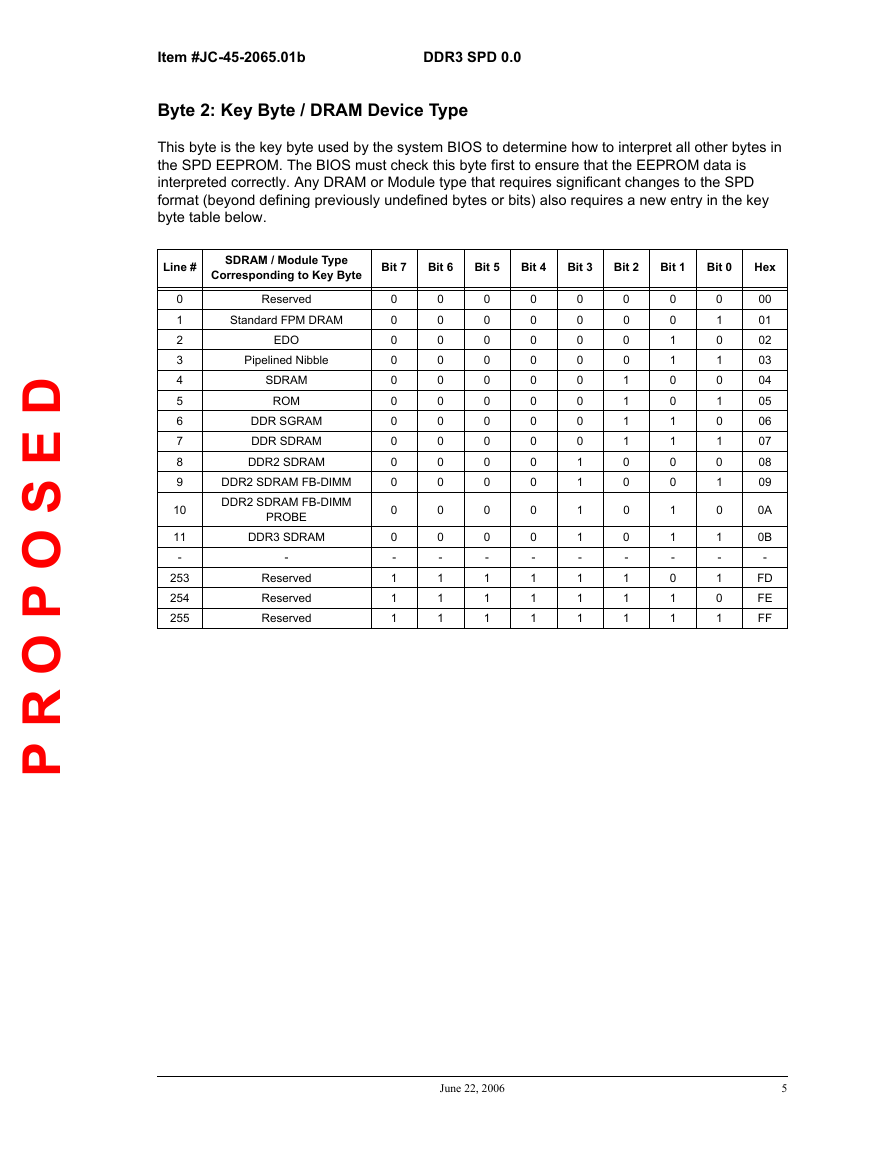
Byte 2: Key Byte / DRAM Device Type
This byte is the key byte used by the system BIOS to determine how to interpret all other bytes in
the SPD EEPROM. The BIOS must check this byte first to ensure that the EEPROM data is
interpreted correctly. Any DRAM or Module type that requires significant changes to the SPD
format (beyond defining previously undefined bytes or bits) also requires a new entry in the key
byte table below.
Line #
SDRAM / Module Type
Corresponding to Key Byte
Bit 7
Bit 6
Bit 5
Bit 4
Bit 3
Bit 2
Bit 1
Bit 0
Hex
0
1
2
3
4
5
6
7
8
9
10
11
-
253
254
255
Reserved
Standard FPM DRAM
EDO
Pipelined Nibble
SDRAM
ROM
DDR SGRAM
DDR SDRAM
DDR2 SDRAM
DDR2 SDRAM FB-DIMM
DDR2 SDRAM FB-DIMM
PROBE
DDR3 SDRAM
-
Reserved
Reserved
Reserved
0
0
0
0
0
0
0
0
0
0
0
0
-
1
1
1
0
0
0
0
0
0
0
0
0
0
0
0
-
1
1
1
0
0
0
0
0
0
0
0
0
0
0
0
-
1
1
1
0
0
0
0
0
0
0
0
0
0
0
0
-
1
1
1
0
0
0
0
0
0
0
0
1
1
1
1
-
1
1
1
0
0
0
0
1
1
1
1
0
0
0
0
-
1
1
1
0
0
1
1
0
0
1
1
0
0
1
1
-
0
1
1
0
1
0
1
0
1
0
1
0
1
0
1
-
1
0
1
00
01
02
03
04
05
06
07
08
09
0A
0B
-
FD
FE
FF
June 22, 2006
5
�
D
E
S
O
P
O
R
P
Item #JC-45-2065.01b
DDR3 SPD 0.0
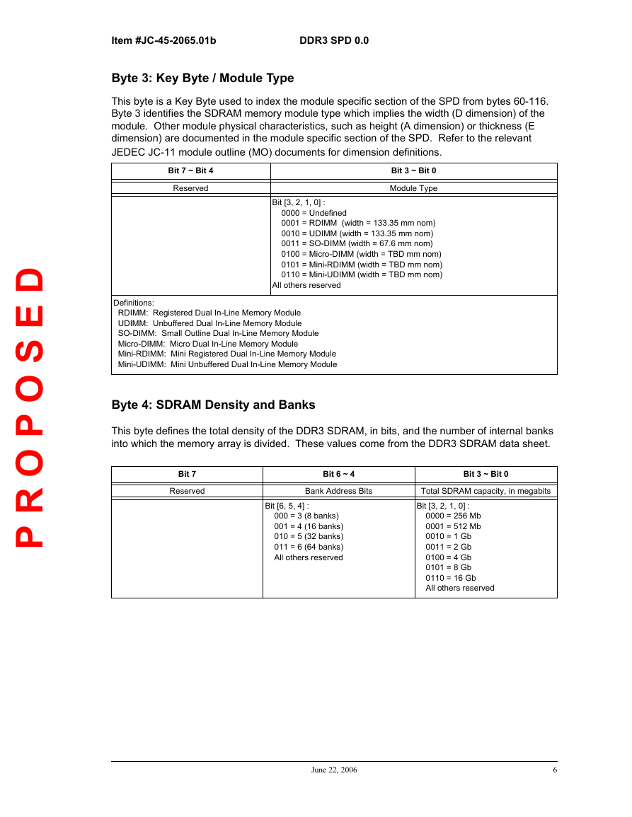
Byte 3: Key Byte / Module Type
This byte is a Key Byte used to index the module specific section of the SPD from bytes 60-116.
Byte 3 identifies the SDRAM memory module type which implies the width (D dimension) of the
module. Other module physical characteristics, such as height (A dimension) or thickness (E
dimension) are documented in the module specific section of the SPD. Refer to the relevant
JEDEC JC-11 module outline (MO) documents for dimension definitions.
Bit 7 ~ Bit 4
Reserved
Bit 3 ~ Bit 0
Module Type
Bit [3, 2, 1, 0] :
0000 = Undefined
0001 = RDIMM (width = 133.35 mm nom)
0010 = UDIMM (width = 133.35 mm nom)
0011 = SO-DIMM (width = 67.6 mm nom)
0100 = Micro-DIMM (width = TBD mm nom)
0101 = Mini-RDIMM (width = TBD mm nom)
0110 = Mini-UDIMM (width = TBD mm nom)
All others reserved
Definitions:
RDIMM: Registered Dual In-Line Memory Module
UDIMM: Unbuffered Dual In-Line Memory Module
SO-DIMM: Small Outline Dual In-Line Memory Module
Micro-DIMM: Micro Dual In-Line Memory Module
Mini-RDIMM: Mini Registered Dual In-Line Memory Module
Mini-UDIMM: Mini Unbuffered Dual In-Line Memory Module
Byte 4: SDRAM Density and Banks
This byte defines the total density of the DDR3 SDRAM, in bits, and the number of internal banks
into which the memory array is divided. These values come from the DDR3 SDRAM data sheet.
Bit 7
Reserved
Bit 6 ~ 4
Bank Address Bits
Bit [6, 5, 4] :
000 = 3 (8 banks)
001 = 4 (16 banks)
010 = 5 (32 banks)
011 = 6 (64 banks)
All others reserved
Bit 3 ~ Bit 0
Total SDRAM capacity, in megabits
Bit [3, 2, 1, 0] :
0000 = 256 Mb
0001 = 512 Mb
0010 = 1 Gb
0011 = 2 Gb
0100 = 4 Gb
0101 = 8 Gb
0110 = 16 Gb
All others reserved
June 22, 2006
6
�
D
E
S
O
P
O
R
P
Item #JC-45-2065.01b
DDR3 SPD 0.0
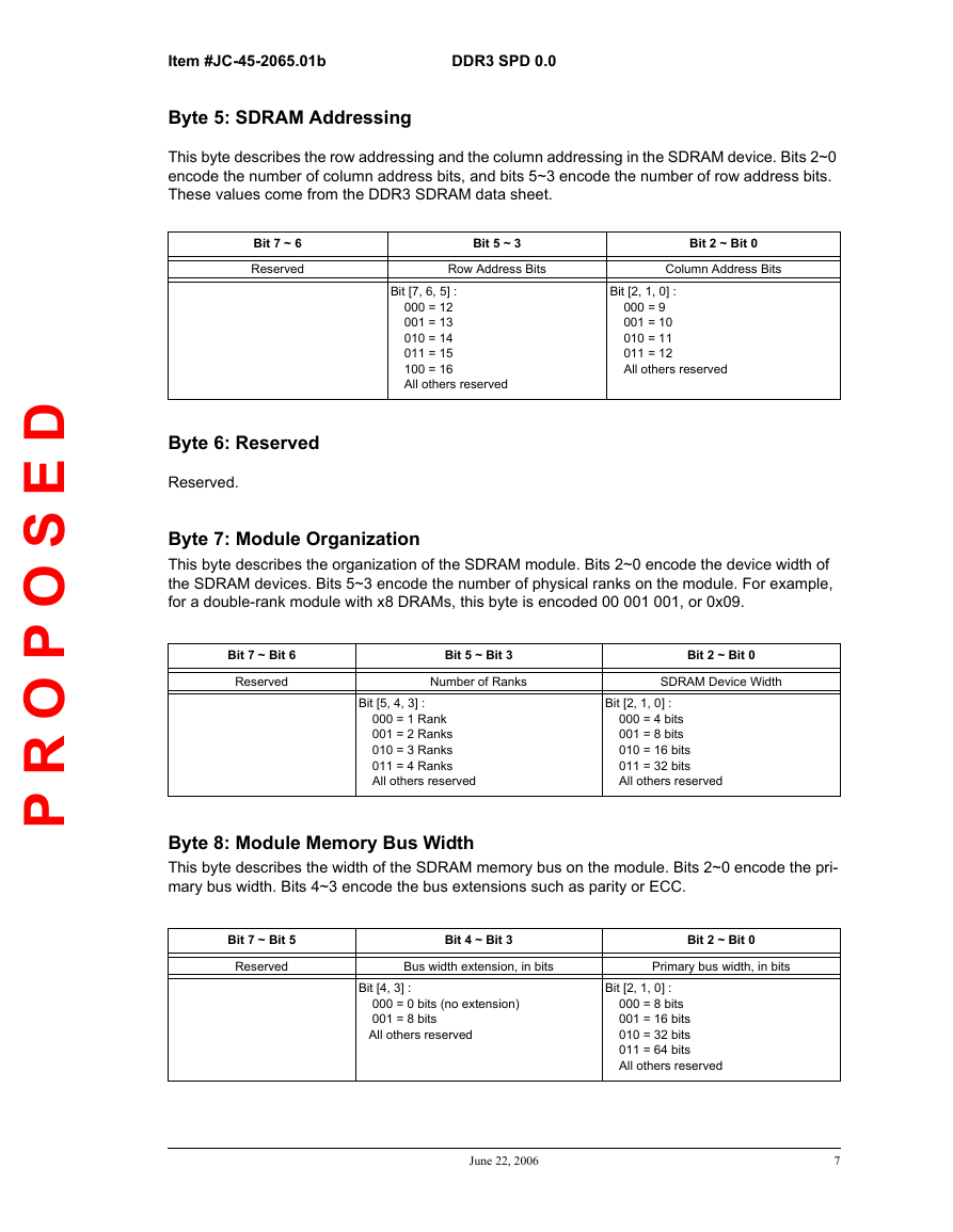
Byte 5: SDRAM Addressing
This byte describes the row addressing and the column addressing in the SDRAM device. Bits 2~0
encode the number of column address bits, and bits 5~3 encode the number of row address bits.
These values come from the DDR3 SDRAM data sheet.
Bit 7 ~ 6
Reserved
Bit 5 ~ 3
Row Address Bits
Bit 2 ~ Bit 0
Column Address Bits
Bit [7, 6, 5] :
000 = 12
001 = 13
010 = 14
011 = 15
100 = 16
All others reserved
Bit [2, 1, 0] :
000 = 9
001 = 10
010 = 11
011 = 12
All others reserved
Byte 6: Reserved
Reserved.
Byte 7: Module Organization
This byte describes the organization of the SDRAM module. Bits 2~0 encode the device width of
the SDRAM devices. Bits 5~3 encode the number of physical ranks on the module. For example,
for a double-rank module with x8 DRAMs, this byte is encoded 00 001 001, or 0x09.
Bit 7 ~ Bit 6
Reserved
Bit 5 ~ Bit 3
Number of Ranks
Bit 2 ~ Bit 0
SDRAM Device Width
Bit [5, 4, 3] :
000 = 1 Rank
001 = 2 Ranks
010 = 3 Ranks
011 = 4 Ranks
All others reserved
Bit [2, 1, 0] :
000 = 4 bits
001 = 8 bits
010 = 16 bits
011 = 32 bits
All others reserved
Byte 8: Module Memory Bus Width
This byte describes the width of the SDRAM memory bus on the module. Bits 2~0 encode the pri-
mary bus width. Bits 4~3 encode the bus extensions such as parity or ECC.
Bit 7 ~ Bit 5
Reserved
Bit 4 ~ Bit 3
Bit 2 ~ Bit 0
Bus width extension, in bits
Primary bus width, in bits
Bit [4, 3] :
000 = 0 bits (no extension)
001 = 8 bits
All others reserved
Bit [2, 1, 0] :
000 = 8 bits
001 = 16 bits
010 = 32 bits
011 = 64 bits
All others reserved
June 22, 2006
7
�
D
E
S
O
P
O
R
P
Item #JC-45-2065.01b
DDR3 SPD 0.0
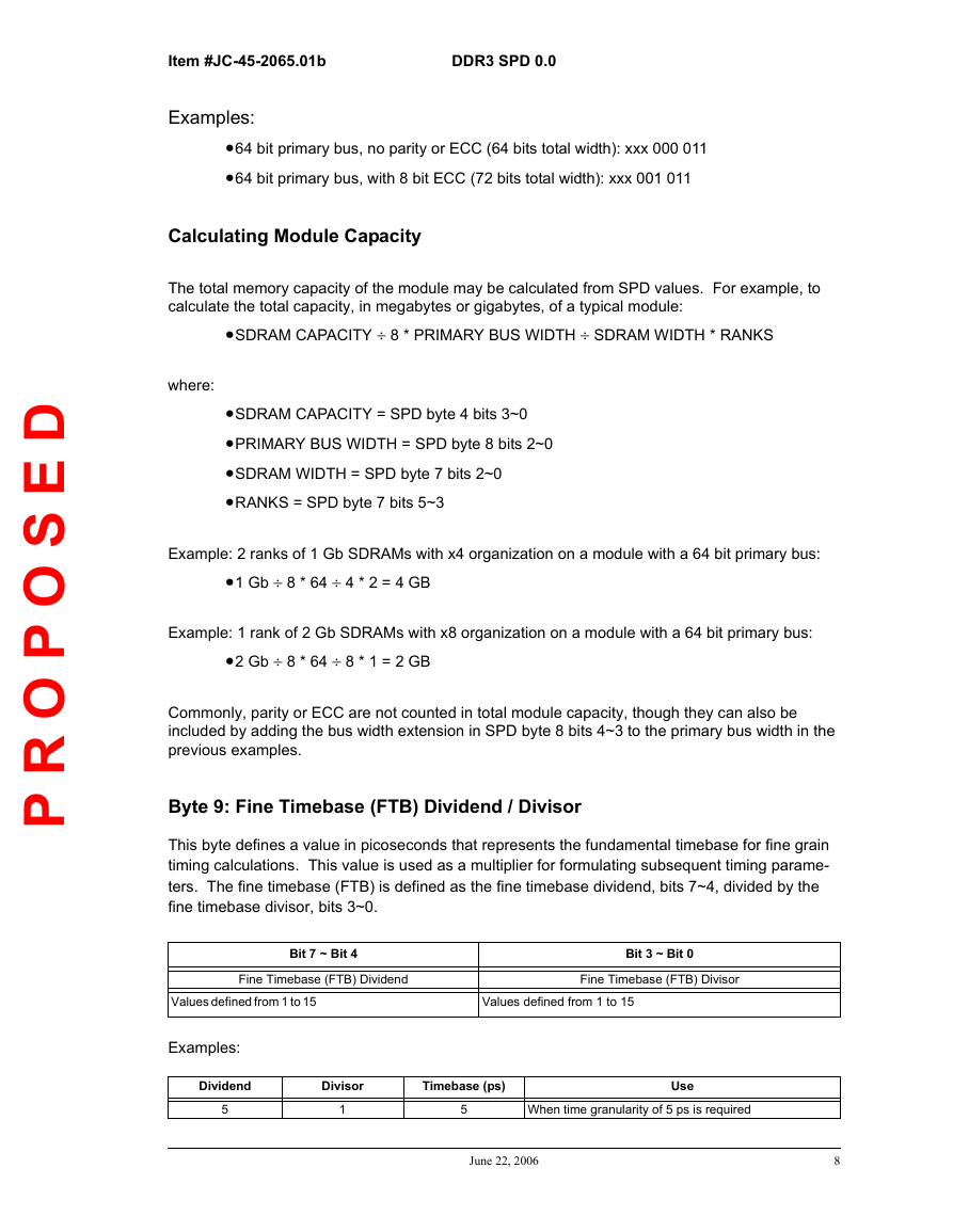
Examples:
•64 bit primary bus, no parity or ECC (64 bits total width): xxx 000 011
64 bit primary bus, with 8 bit ECC (72 bits total width): xxx 001 011
Calculating Module Capacity
The total memory capacity of the module may be calculated from SPD values. For example, to
calculate the total capacity, in megabytes or gigabytes, of a typical module:
SDRAM CAPACITY ÷ 8 * PRIMARY BUS WIDTH ÷ SDRAM WIDTH * RANKS
where:
SDRAM CAPACITY = SPD byte 4 bits 3~0
PRIMARY BUS WIDTH = SPD byte 8 bits 2~0
SDRAM WIDTH = SPD byte 7 bits 2~0
RANKS = SPD byte 7 bits 5~3
Example: 2 ranks of 1 Gb SDRAMs with x4 organization on a module with a 64 bit primary bus:
1 Gb ÷ 8 * 64 ÷ 4 * 2 = 4 GB
Example: 1 rank of 2 Gb SDRAMs with x8 organization on a module with a 64 bit primary bus:
2 Gb ÷ 8 * 64 ÷ 8 * 1 = 2 GB
Commonly, parity or ECC are not counted in total module capacity, though they can also be
included by adding the bus width extension in SPD byte 8 bits 4~3 to the primary bus width in the
previous examples.
Byte 9: Fine Timebase (FTB) Dividend / Divisor
This byte defines a value in picoseconds that represents the fundamental timebase for fine grain
timing calculations. This value is used as a multiplier for formulating subsequent timing parame-
ters. The fine timebase (FTB) is defined as the fine timebase dividend, bits 7~4, divided by the
fine timebase divisor, bits 3~0.
Bit 7 ~ Bit 4
Bit 3 ~ Bit 0
Fine Timebase (FTB) Dividend
Fine Timebase (FTB) Divisor
Values defined from 1 to 15 Values defined from 1 to 15
Examples:
Dividend
5
Divisor
1
Timebase (ps)
Use
5
When time granularity of 5 ps is required
June 22, 2006
8
�


 2023年江西萍乡中考道德与法治真题及答案.doc
 2012年重庆南川中考生物真题及答案.doc
 2013年江西师范大学地理学综合及文艺理论基础考研真题.doc
 2020年四川甘孜小升初语文真题及答案I卷.doc
 2020年注册岩土工程师专业基础考试真题及答案.doc
 2023-2024学年福建省厦门市九年级上学期数学月考试题及答案.doc
 2021-2022学年辽宁省沈阳市大东区九年级上学期语文期末试题及答案.doc
 2022-2023学年北京东城区初三第一学期物理期末试卷及答案.doc
 2018上半年江西教师资格初中地理学科知识与教学能力真题及答案.doc
 2012年河北国家公务员申论考试真题及答案-省级.doc
 2020-2021学年江苏省扬州市江都区邵樊片九年级上学期数学第一次质量检测试题及答案.doc
 2022下半年黑龙江教师资格证中学综合素质真题及答案.doc