letters to nature
20. Pavlov, V. V., Pisarev, R. V., Kirilyuk, A. & Rasing, T. Observation of a transversal nonlinear magneto-
optical effect in thin magnetic garnet films. Phys. Rev. Lett. 78, 2004–2007 (1997).
21. Novoselov, K. S., Geim, A. K., van der Berg, D., Dubonos, S. V. & Maan, J. C. Domain wall
propagation on nanometer scale: coercivity of a single pinning center. IEEE Trans. Magn. 38,
2583–2585 (2002).
22. Peeters, F. M. & Li, X. Q. Hall magnetometer in the ballistic regime. Appl. Phys. Lett. 72, 572–574
(1998).
23. Kent, A. D., von Molnar, S., Gider, S. & Awschalom, D. D. Properties and measurement of
scanning tunneling microscope fabricated ferromagnetic particle arrays. J. Appl. Phys. 76, 6656–6660
(1994).
24. Li, Y. Q. et al. Hall magnetometry on a single iron nanoparticle. Appl. Phys. Lett. 80, 4644–4646
(2002).
25. Hengstmann, T. M., Grundler, D., Heyn, C. & Heitmann, D. Stray-field investigation on permalloy
nanodisks. J. Appl. Phys. 90, 6542–6544 (2001).
26. Schuh, D., Biberger, J., Bauer, A., Breuer, W. & Weiss, D. Hall-magnetometry on ferromagnetic dots
and dot arrays. IEEE Trans. Magn. 37, 2091–2093 (2001).
27. Vergne, R., Cotillard, J. C. & Porteseil, J. L. Some statistical aspects of magnetization processes in
ferromagnetic bodies—motion of a single 180-degrees Bloch wall in an imperfect crystalline medium.
Rev. Phys. Appl. 16, 449–476 (1981).
28. Wunderlich, J. et al. Influence of geometry on domain wall propagation in a mesoscopic wire. IEEE
Trans. Magn. 37, 2104–2107 (2001).
29. Kim, D. H., Choe, S. B. & Shin, S. C. Direct observation of Barkhausen avalanche in Co thin films.
Phys. Rev. Lett. 90, 087203 (2003).
30. Magnus, K. Vibrations (Blackie & Son, London, 1965).
31. Acheson, D. From Calculus to Chaos (Oxford Univ. Press, Oxford, 1997).
Acknowledgements This research was supported by the EPSRC (UK). We thank S. Gillott and
M. Sellers for technical assistance and J. Steeds for advice on dislocation motion. S.V.D. also
acknowledges support from Russian Ministry of Science and Technology.
Competing interests statement The authors declare that they have no competing financial
interests.
Correspondence and requests for materials should be addressed to A.K.G. (geim@man.ac.uk).
..............................................................
Subwavelength-diameter silica wires
for low-loss optical wave guiding
Limin Tong1,2, Rafael R. Gattass1, Jonathan B. Ashcom1*, Sailing He2,
Jingyi Lou2, Mengyan Shen1,3, Iva Maxwell1 & Eric Mazur1
1Department of Physics and Division of Engineering and Applied Sciences,
Harvard University, Cambridge, Massachusetts 02138, USA
2Centre for Optical and Electromagnetic Research and Department of Physics,
Zhejiang University, Hangzhou 310027, China
3Department of Physics, Graduate School of Science, Tohoku University, Sendai,
Miyagi 9808578, Japan
* Present address: Lincoln Laboratory, Massachusetts Institute of Technology, Lexington, Massachusetts
02420, USA
.............................................................................................................................................................................
Silica waveguides with diameters larger than the wavelength of
transmitted light are widely used in optical communications,
sensors and other applications1–3. Minimizing the width of the
waveguides is desirable for photonic device applications, but the
fabrication of low-loss optical waveguides with subwavelength
diameters remains challenging because of strict requirements on
surface roughness and diameter uniformity4–7. Here we report
the fabrication of subwavelength-diameter silica ‘wires’ for use as
low-loss optical waveguides within the visible to near-infrared
spectral range. We use a two-step drawing process to fabricate
long free-standing silica wires with diameters down to 50 nm that
show surface smoothness at the atomic level together with
uniformity of diameter. Light can be launched into these wires
by optical evanescent coupling. The wires allow single-mode
operation, and have an optical loss of less than 0.1 dB mm21.
We believe that these wires provide promising building blocks for
future microphotonic devices with subwavelength-width
structures.
The fabrication of thin silica wires was first investigated in the
nineteenth century, when the mechanical properties of the wires
were studied, but their optical properties and applications remained
uninvestigated8,9. It was not until a century later that researchers
began to investigate the optical applications of silica wires made by
drawing high-purity glass fibres from a laser-heated melt10–14. With
a diameter of more than one micrometre, these silica wires allow
multimode waveguiding of visible and infrared light. Submicro-
metre wires allow single-mode operation, but both theoretical and
experimental results show that the laser power required for drawing
silica submicrometre- or nanometre-diameter wires (SMNWs) with
a uniform diameter is impractically large14,15. When drawing wires
from a flame-heated melt, turbulence and convection make it
difficult to control the temperature gradient in the drawing region,
and consequently size uniformity is difficult to maintain when the
wire diameter is reduced to less than one micrometre. Silica
nanowires with diameters ranging from ten to several hundred
nanometres have recently been obtained with other methods16–18,
but the diameter fluctuation and sidewall roughness of those wires
makes them unsuitable for low-loss optical wave guiding.
Here we introduce a two-step drawing process for fabricating
long uniform silica SMNWs by a flame-heated fibre drawing
method. First, we use a flame to draw a silica fibre to a micro-
metre-diameter wire. Second, to obtain a steady temperature
distribution in the drawing region while further reducing the wire
diameter, we use a tapered sapphire fibre with a tip diameter of
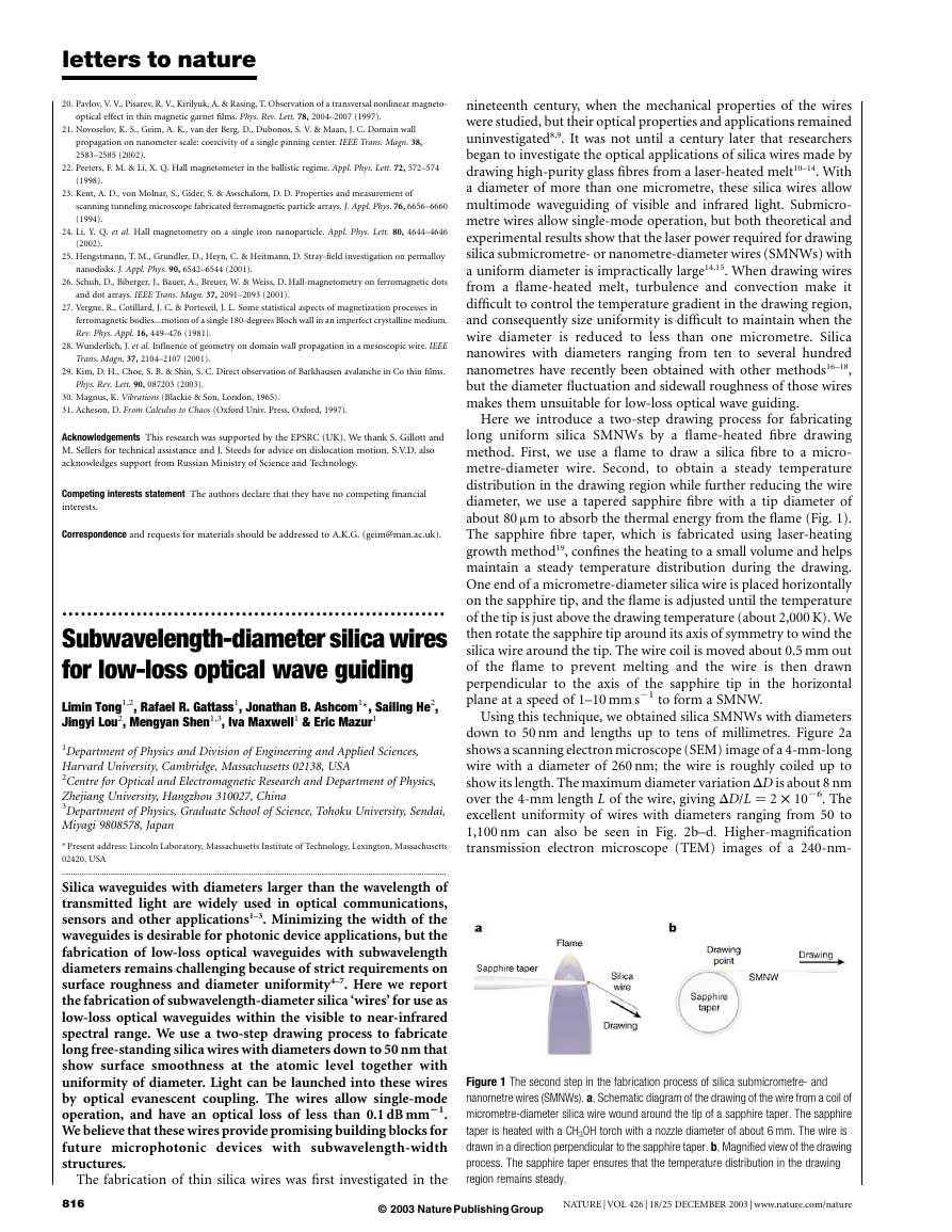
about 80 m m to absorb the thermal energy from the flame (Fig. 1).
The sapphire fibre taper, which is fabricated using laser-heating
growth method19, confines the heating to a small volume and helps
maintain a steady temperature distribution during the drawing.
One end of a micrometre-diameter silica wire is placed horizontally
on the sapphire tip, and the flame is adjusted until the temperature
of the tip is just above the drawing temperature (about 2,000 K). We
then rotate the sapphire tip around its axis of symmetry to wind the
silica wire around the tip. The wire coil is moved about 0.5 mm out
of the flame to prevent melting and the wire is then drawn
perpendicular to the axis of the sapphire tip in the horizontal
plane at a speed of 1–10 mm s21 to form a SMNW.
Using this technique, we obtained silica SMNWs with diameters
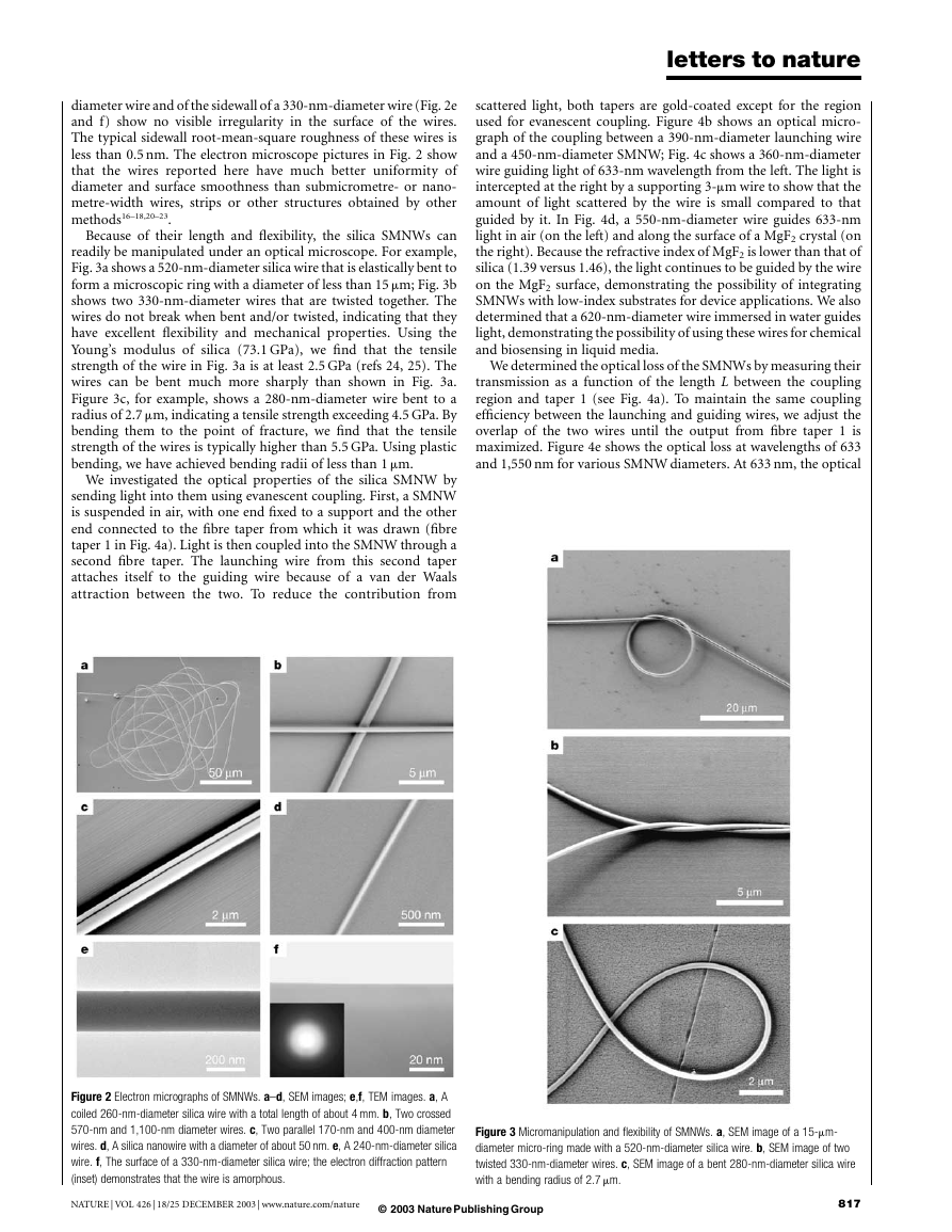
down to 50 nm and lengths up to tens of millimetres. Figure 2a
shows a scanning electron microscope (SEM) image of a 4-mm-long
wire with a diameter of 260 nm; the wire is roughly coiled up to
show its length. The maximum diameter variation DD is about 8 nm
over the 4-mm length L of the wire, giving DD/L ¼ 2 £ 1026. The
excellent uniformity of wires with diameters ranging from 50 to
1,100 nm can also be seen in Fig. 2b–d. Higher-magnification
transmission electron microscope (TEM) images of a 240-nm-
Figure 1 The second step in the fabrication process of silica submicrometre- and
nanometre wires (SMNWs). a, Schematic diagram of the drawing of the wire from a coil of
micrometre-diameter silica wire wound around the tip of a sapphire taper. The sapphire
taper is heated with a CH3OH torch with a nozzle diameter of about 6 mm. The wire is
drawn in a direction perpendicular to the sapphire taper. b, Magnified view of the drawing
process. The sapphire taper ensures that the temperature distribution in the drawing
region remains steady.
816
© 2003 Nature Publishing Group
NATURE | VOL 426 | 18/25 DECEMBER 2003 | www.nature.com/nature
�
letters to nature
scattered light, both tapers are gold-coated except for the region
used for evanescent coupling. Figure 4b shows an optical micro-
graph of the coupling between a 390-nm-diameter launching wire
and a 450-nm-diameter SMNW; Fig. 4c shows a 360-nm-diameter
wire guiding light of 633-nm wavelength from the left. The light is
intercepted at the right by a supporting 3-m m wire to show that the
amount of light scattered by the wire is small compared to that
guided by it. In Fig. 4d, a 550-nm-diameter wire guides 633-nm
light in air (on the left) and along the surface of a MgF2 crystal (on
the right). Because the refractive index of MgF2 is lower than that of
silica (1.39 versus 1.46), the light continues to be guided by the wire
on the MgF2 surface, demonstrating the possibility of integrating
SMNWs with low-index substrates for device applications. We also
determined that a 620-nm-diameter wire immersed in water guides
light, demonstrating the possibility of using these wires for chemical
and biosensing in liquid media.
We determined the optical loss of the SMNWs by measuring their
transmission as a function of the length L between the coupling
region and taper 1 (see Fig. 4a). To maintain the same coupling
efficiency between the launching and guiding wires, we adjust the
overlap of the two wires until the output from fibre taper 1 is
maximized. Figure 4e shows the optical loss at wavelengths of 633
and 1,550 nm for various SMNW diameters. At 633 nm, the optical
diameter wire and of the sidewall of a 330-nm-diameter wire (Fig. 2e
and f) show no visible irregularity in the surface of the wires.
The typical sidewall root-mean-square roughness of these wires is
less than 0.5 nm. The electron microscope pictures in Fig. 2 show
that the wires reported here have much better uniformity of
diameter and surface smoothness than submicrometre- or nano-
metre-width wires, strips or other structures obtained by other
methods16–18,20–23.
Because of their length and flexibility, the silica SMNWs can
readily be manipulated under an optical microscope. For example,
Fig. 3a shows a 520-nm-diameter silica wire that is elastically bent to
form a microscopic ring with a diameter of less than 15 m m; Fig. 3b
shows two 330-nm-diameter wires that are twisted together. The
wires do not break when bent and/or twisted, indicating that they
have excellent flexibility and mechanical properties. Using the
Young’s modulus of silica (73.1 GPa), we find that the tensile
strength of the wire in Fig. 3a is at least 2.5 GPa (refs 24, 25). The
wires can be bent much more sharply than shown in Fig. 3a.
Figure 3c, for example, shows a 280-nm-diameter wire bent to a
radius of 2.7 m m, indicating a tensile strength exceeding 4.5 GPa. By
bending them to the point of fracture, we find that the tensile
strength of the wires is typically higher than 5.5 GPa. Using plastic
bending, we have achieved bending radii of less than 1 m m.
We investigated the optical properties of the silica SMNW by
sending light into them using evanescent coupling. First, a SMNW
is suspended in air, with one end fixed to a support and the other
end connected to the fibre taper from which it was drawn (fibre
taper 1 in Fig. 4a). Light is then coupled into the SMNW through a
second fibre taper. The launching wire from this second taper
attaches itself to the guiding wire because of a van der Waals
attraction between the two. To reduce the contribution from
Figure 2 Electron micrographs of SMNWs. a–d, SEM images; e,f, TEM images. a, A
coiled 260-nm-diameter silica wire with a total length of about 4 mm. b, Two crossed
570-nm and 1,100-nm diameter wires. c, Two parallel 170-nm and 400-nm diameter
wires. d, A silica nanowire with a diameter of about 50 nm. e, A 240-nm-diameter silica
wire. f, The surface of a 330-nm-diameter silica wire; the electron diffraction pattern
(inset) demonstrates that the wire is amorphous.
Figure 3 Micromanipulation and flexibility of SMNWs. a, SEM image of a 15-m m-
diameter micro-ring made with a 520-nm-diameter silica wire. b, SEM image of two
twisted 330-nm-diameter wires. c, SEM image of a bent 280-nm-diameter silica wire
with a bending radius of 2.7 m m.
NATURE | VOL 426 | 18/25 DECEMBER 2003 | www.nature.com/nature
© 2003 Nature Publishing Group
817
�
letters to nature
loss of a 190-nm-diameter wire is about 1.7 dB mm21, which is
much lower than the optical loss of other subwavelength-structures
such as metallic plasmon waveguides26–28.
The increasing loss with decreasing wire diameter can be attrib-
uted to surface contamination: as the wire diameter is reduced
below the wavelength, more light is guided outside the wire as an
evanescent wave and becomes susceptible to scattering by surface
contamination. Calculations show that the critical diameter for
single-mode operation of a silica wire is about 450 nm at 633-nm
wavelength and 1,100 nm at 1,550-nm wavelength29, and that about
20% of the energy propagates outside the silica core under those
conditions. Figure 4e shows that wires with these diameters have an
optical loss below 0.1 dB mm21. For smaller diameters, more light
propagates outside the silica core as an evanescent wave. Evanescent
wave propagation is extremely useful for enhancing the perform-
ance of devices such as optical sensors.
Because of the large index contrast between silica and air, silica
SMNWs can be bent sharply without incurring large bending
losses. Using a three-dimensional finite-difference time domain
simulation30, we find a bending loss of less than 0.3 dB for a 908
turn with a bending radius of 5 m m in an air-clad 450-nm-diameter
silica wire (for light of 633-nm wavelength). These results indicate
that the silica SMNWs are also suitable for applications where tight
waveguide bends are desired. Using two probes from a scanning
tunnelling microscope for micromanipulation, we were able to
successfully guide 633-nm wavelength light through a bend with a
5.6-m m radius in a silica wire with a diameter of about 510 nm (see
Fig. 4f). As can be seen in the figure, the intensity of scattered light
after the bend is not greatly reduced, indicating that the bending loss
is low. The ability to guide light through sharp bends is especially
useful for miniaturization of photonic devices. Also, with low
bending loss, micro-rings made from these wires (such as the one
shown in Fig. 3a) can be incorporated into photonic devices such as
optical microresonators for optical communication or optical
sensing. For example, we used a 950-nm-diameter SMNW to
make a ring with a 75-m m radius similar to the one shown in
Fig. 3a; preliminary measurements show that the ring has Q factor
of about 1,500 at a wavelength of 1,550 nm.
Figure 4 Optical characterization of SMNWs. a, Schematic diagram for launching light
into a silica wire using evanescent coupling. b, Optical microscope image of a 390-nm-
diameter taper coupling light into a 450-nm-diameter silica wire. c, Long-time exposure
micrograph of 633-nm wavelength light guided by a 360-nm-diameter silica wire in air,
and intercepted by a 3-m m guiding wire on the right. d, Optical microscope image of
633-nm-wavelength light guided by a 550-nm-diameter silica wire with its left half
suspended in air and its right half placed on a MgF2 crystal. e, Measured optical loss of
silica wires at 633 nm (filled blue circles) and 1,550 nm (filled yellow circles). f, Optical
microscope image of 633-nm light travelling through a sharp bend with a radius of 5.6 m m
in a 510-nm-wide silica wire.
818
© 2003 Nature Publishing Group
NATURE | VOL 426 | 18/25 DECEMBER 2003 | www.nature.com/nature
�
The wires reported here are suitable for low-loss optical wave
guiding, and will be promising components in future micropho-
tonic devices for various applications, such as optical communi-
cations and optical sensing. Owing to their excellent uniformity,
large length, high flexibility, and strength, these wires can be
manipulated and assembled with high accuracy and used as
micro- or nanoscale tools in physical, chemical, biological, micro-
A
electronic and materials research.
Received 22 August; accepted 4 November 2003; doi:10.1038/nature02193.
1. Yamane, M. & Asahara, Y. Glasses for Photonics (Cambridge Univ. Press, Cambridge, UK, 2000).
2. Murata, H. Handbook of Optical Fibers and Cables 2nd edn (Marcel Dekker, New York, 1996).
3. Mynbaev, D. K. & Scheiner, L. L. Fiber-Optic Communications Technology (Prentice Hall, New York,
2001).
4. Marcuse, D. Mode conversion caused by surface imperfections of a dielectric slab waveguide. Bell Syst.
Tech. J. 48, 3187–3215 (1969).
5. Marcuse, D. & Derosier, R. M. Mode conversion caused by diameter changes of a round dielectric
waveguide. Bell Syst. Tech. J. 48, 3217–3232 (1969).
6. Ladouceur, F. Roughness, inhomogeneity, and integrated optics. J. Lightwave Technol. 15, 1020–1025
(1997).
7. Lee, K. K. et al. Effect of size and roughness on light transmission in a Si/SiO2 waveguide:
experiments and model. Appl. Phys. Lett. 77, 1617–1619 (2000). Erratum. Appl. Phys. Lett. 77, 2258
(2000).
8. Boys, C. V. On the production, properties, and some suggested uses of the finest threads. Phil. Mag. 23,
489–499 (1887).
9. Threlfall, R. On Laboratory Arts (Macmillan, London, 1898).
10. Knight, J. C., Cheung, G., Jacques, F. & Birks, T. A. Phase-matched excitation of whispering-gallery-
mode resonances by a fiber taper. Opt. Lett. 22, 1129–1131 (1997).
11. Birks, T. A., Wadsworth, W. J. & Russell, P. St. J. Supercontinuum generation in tapered fibers. Opt.
Lett. 25, 1415–1417 (2000).
12. Cai, M. & Vahala, K. Highly efficient hybrid fiber taper coupled microsphere laser. Opt. Lett. 26,
884–886 (2001).
13. Kakarantzas, G., Dimmick, T. E., Birks, T. A., Le Roux, R. & Russell, P. St. J. Miniature all-fiber devices
based on CO2 laser microstructuring of tapered fibers. Opt. Lett. 26, 1137–1139 (2001).
14. Dimmick, T. E., Kakarantzas, G., Birks, T. A. & Russell, P. St. J. Carbon dioxide laser fabrication of
fused-fiber couplers and tapers. Appl. Opt. 38, 6845–6848 (1999).
15. Grellier, A. J. C., Zayer, N. K. & Pannell, C. N. Heat transfer modeling in CO2 laser processing of
optical fibres. Opt. Commun. 152, 324–328 (1998).
16. Wang, Z. L., Gao, R. P. P., Gole, J. L. & Stout, J. D. Silica nanotubes and nanofiber arrays. Adv. Mater.
12, 1938–1940 (2000).
17. Pan, Z. W., Dai, Z. R., Ma, C. & Wang, Z. L. Molten gallium as a catalyst for the large-scale growth of
highly aligned silica nanowires. J. Am. Chem. Soc. 124, 1817–1822 (2002).
18. Hu, J. Q., Meng, X. M., Jiang, Y., Lee, C. S. & Lee, S. T. Fabrication of germanium-filled silica
nanotubes and aligned silica nanofibers. Adv. Mater. 15, 70–73 (2003).
19. Labelle, H. E. & Mlavsky, A. I. Growth of sapphire filaments from melt. Nature 216, 574–575
(1967).
20. Morales, A. M. & Lieber, C. M. A laser ablation method for the synthesis of crystalline semiconductor
nanowires. Science 279, 208–211 (1998).
21. Xia, Y., Rogers, J. A., Paul, K. E. & Whitesides, G. M. Unconventional methods for fabricating and
patterning nanostructures. Chem. Rev. 99, 1823–1848 (1999).
22. Ito, T. & Okazaki, S. Pushing the limits of lithography. Nature 406, 1027–1031 (2000).
23. Lee, K. K., Lim, D. R., Kimerling, L. C., Shin, J. & Cerrina, F. Fabrication of ultralow-loss Si/SiO2
waveguides by roughness reduction. Opt. Lett. 26, 1888–1890 (2001).
24. Matthewson, M. J., Kurkjian, C. R. & Gulati, S. T. Strength measurement of optical fibers by bending.
J. Am. Ceram. Soc. 69, 815–821 (1986).
25. Krause, J. T., Testardi, L. R. & Thurston, R. N. Deviations from linearity in the dependence of
elongation upon force for fibers of simple glass formers and of glass optical light guides. Phys. Chem.
Glasses 20, 135–139 (1979).
26. Takahara, J., Yamagishi, S., Taki, H., Morimoto, A. & Kobayashi, T. Guiding of a one-dimensional
optical beam with nanometer diameter. Opt. Lett. 22, 475–477 (1997).
27. Maier, S. A., Kik, P. G. & Atwater, H. A. Observation of coupled plasmon-polarization modes in Au
nanoparticle chain waveguides of different lengths: Estimation of waveguide loss. Appl. Phys. Lett. 81,
1714–1716 (2002).
28. Maier, S. A. et al. Local detection of electromagnetic energy transport below the diffraction limit in
metal nanoparticle plasmon waveguides. Nature Mater. 2, 229–232 (2003).
29. Snyder, A. W. & Love, J. D. Optical Waveguide Theory (Chapman and Hall, New York, 1983).
30. Taflove, A. Computational Electrodynamics: The Finite-difference Time-domain Method (Artech
House, Boston, 1995).
Acknowledgements We thank Y. Lu, Z. Han and B. Tull for assistance in SEM and TEM imaging,
and L. Liu and X. Chen for help with numerical simulations. This work was supported by the US
National Science Foundation and by the National Natural Science Foundation in China.
T.L. acknowledges support from the Centre for Imaging and Mesoscale Structures at Harvard
University.
Competing interests statement The authors declare that they have no competing financial
interests.
Correspondence and requests for materials should be addressed to E.M.
(mazur@deas.harvard.edu).
letters to nature
..............................................................
Synthesis of a Mo¨bius aromatic
hydrocarbon
D. Ajami1, O. Oeckler2, A. Simon2 & R. Herges1
1Institut fu¨r Organische Chemie, Universita¨t Kiel, Otto-Hahn-Platz 4, 24098 Kiel,
Germany
2Max-Planck-Institut fu¨r Festko¨rperforschung, Heisenbergstraße 1,
D-70569 Stuttgart, Germany
.............................................................................................................................................................................
The defining feature of aromatic hydrocarbon compounds is a
cyclic molecular structure stabilized by the delocalization of p
electrons that, according to the Hu¨ckel rule, need to total 4n 1 2
(n 5 1,2,…); cyclic compounds with 4n p electrons are antiaro-
matic and unstable. But in 1964, Heilbronner predicted1 on
purely theoretical grounds that cyclic molecules with the topol-
ogy of a Mo¨bius band—a ring constructed by joining the ends of a
rectangular strip after having given one end half a twist—should
be aromatic if they contain 4n, rather than 4n 1 2, p electrons.
The prediction stimulated attempts to synthesize Mo¨bius aro-
matic hydrocarbons, but twisted cyclic molecules are destabilized
by large ring strains, with the twist also suppressing overlap of
the p orbitals involved in electron delocalization and stabiliza-
tion. In larger cyclic molecules, ring strain is less pronounced but
the structures are very flexible and flip back to the less-strained
Hu¨ ckel topology2,3. Although transition-state species4, an
unstable intermediate5 and a non-conjugated cyclic molecule6,
all with a Mo¨bius topology, have been documented, a stable
aromatic Mo¨bius system has not yet been realized. Here we report
that combining a ‘normal’ aromatic structure (with p orbitals
orthogonal to the ring plane) and a ‘belt-like’ aromatic structure
(with p orbitals within the ring plane) yields a Mo¨bius compound
stabilized by its extended p system.
Numerous theoretical calculations have been performed to pre-
dict the properties of potential Mo¨bius aromatic systems7–12. The
twist in the p system is usually introduced by a suitable arrangement
of E and Z double bonds. Trans-benzene13 is the smallest conceivable
antiaromatic Mo¨bius annulene. It is only a very shallow minimum
on the energy hypersurface, with an energy as much as
107 kcal mol21 above benzene14. The next-higher Mo¨bius homo-
logue, trans-cyclooctatetraene, indeed comes energetically closer to
its Hu¨ckel (all-cis and global minimum) isomer14. Nevertheless,
with a relative energy of 21.3 kcal mol21, it is expected to be
extremely difficult to synthesize. Moreover, there is almost no
conjugation between the E and the neighbouring Z double bonds
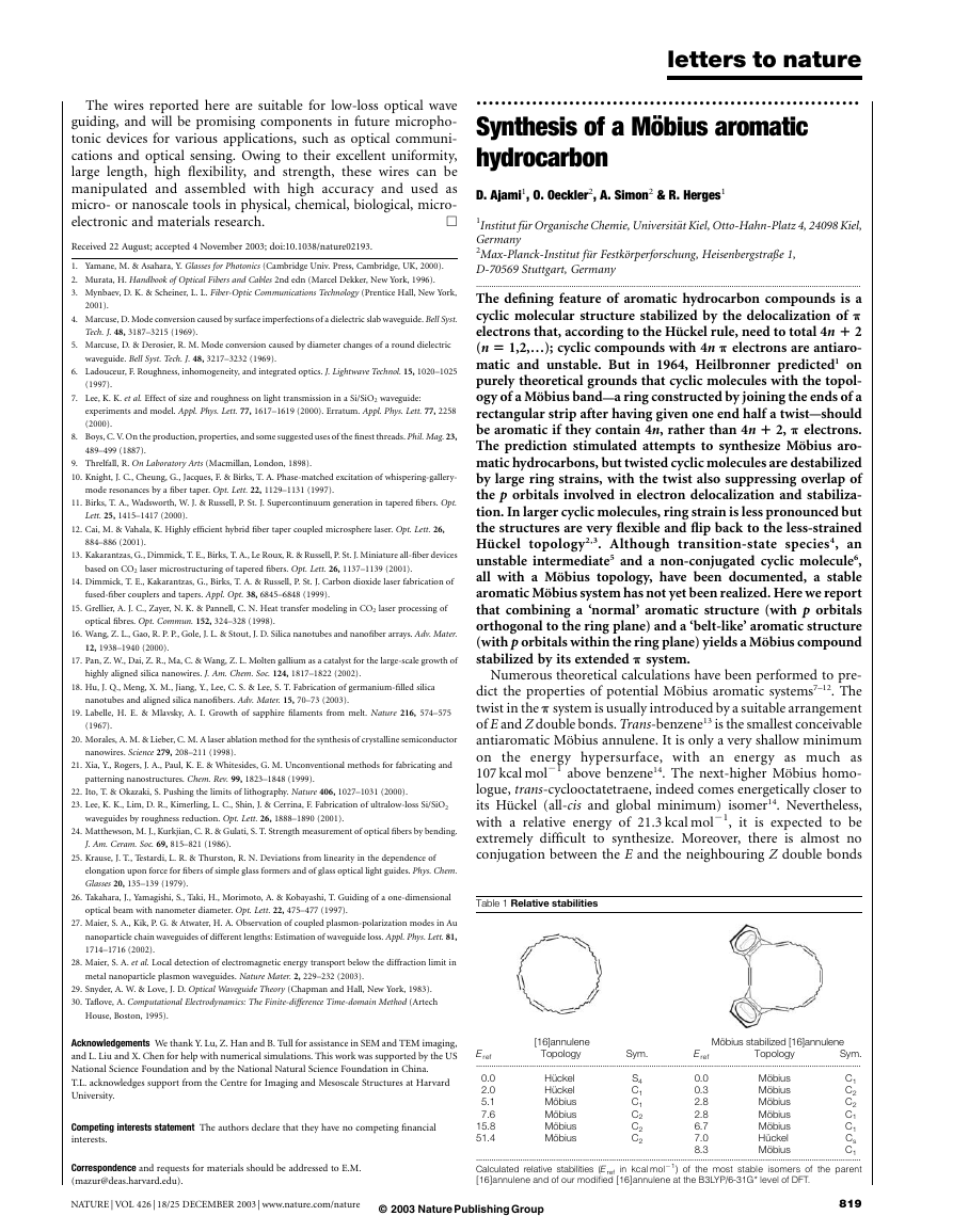
Table 1 Relative stabilities
[16]annulene
Mo¨ bius stabilized [16]annulene
Topology
Sym.
Topology
0.0
2.0
5.1
7.6
15.8
51.4
Sym.
E ref
.............................................................................................................................................................................
C1
C2
C2
C1
C1
Cs
C1
.............................................................................................................................................................................
in kcal mol21) of the most stable isomers of the parent
Calculated relative stabilities (E ref
[16]annulene and of our modified [16]annulene at the B3LYP/6-31G* level of DFT.
Mo¨ bius
Mo¨ bius
Mo¨ bius
Mo¨ bius
Mo¨ bius
Hu¨ ckel
Mo¨ bius
Hu¨ ckel
Hu¨ ckel
Mo¨ bius
Mo¨ bius
Mo¨ bius
Mo¨ bius
E ref
0.0
0.3
2.8
2.8
6.7
7.0
8.3
S4
C1
C1
C2
C2
C2
NATURE | VOL 426 | 18/25 DECEMBER 2003 | www.nature.com/nature
© 2003 Nature Publishing Group
819
�



 2023年江西萍乡中考道德与法治真题及答案.doc
 2012年重庆南川中考生物真题及答案.doc
 2013年江西师范大学地理学综合及文艺理论基础考研真题.doc
 2020年四川甘孜小升初语文真题及答案I卷.doc
 2020年注册岩土工程师专业基础考试真题及答案.doc
 2023-2024学年福建省厦门市九年级上学期数学月考试题及答案.doc
 2021-2022学年辽宁省沈阳市大东区九年级上学期语文期末试题及答案.doc
 2022-2023学年北京东城区初三第一学期物理期末试卷及答案.doc
 2018上半年江西教师资格初中地理学科知识与教学能力真题及答案.doc
 2012年河北国家公务员申论考试真题及答案-省级.doc
 2020-2021学年江苏省扬州市江都区邵樊片九年级上学期数学第一次质量检测试题及答案.doc
 2022下半年黑龙江教师资格证中学综合素质真题及答案.doc