Atlas User’s Manual
Notice
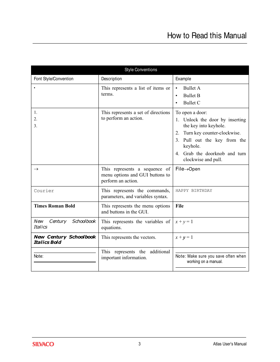
How to Read this Manual
Acknowledgements
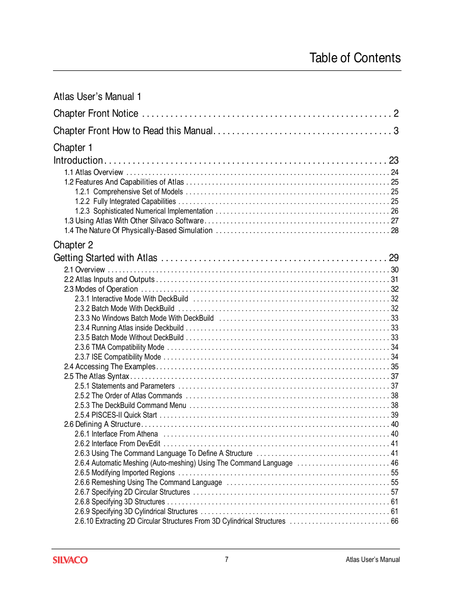
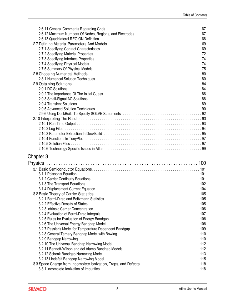
Table of Contents
Chapter 1 Introduction
1.1 Atlas Overview
1.2 Features And Capabilities of Atlas
1.2.1 Comprehensive Set of Models
1.2.2 Fully Integrated Capabilities
1.2.3 Sophisticated Numerical Implementation
1.3 Using Atlas With Other Silvaco Software
1.4 The Nature Of Physically-Based Simulation
Chapter 2 Getting Started with Atlas
2.1 Overview
2.2 Atlas Inputs and Outputs
2.3 Modes of Operation
2.3.1 Interactive Mode With DeckBuild
2.3.2 Batch Mode With DeckBuild
2.3.3 No Windows Batch Mode With DeckBuild
2.3.4 Running Atlas inside Deckbuild
Running a given version number of Atlas
Starting Parallel Atlas
2.3.5 Batch Mode Without DeckBuild
2.3.6 TMA Compatibility Mode
2.3.7 ISE Compatibility Mode
2.4 Accessing The Examples
2.5 The Atlas Syntax
2.5.1 Statements and Parameters
2.5.2 The Order of Atlas Commands
2.5.3 The DeckBuild Command Menu
2.5.4 PISCES-II Quick Start
2.6 Defining A Structure
2.6.1 Interface From Athena
2.6.2 Interface From DevEdit
2.6.3 Using The Command Language To Define A Structure
Specifying The Initial Mesh
Specifying Regions And Materials
Cylindrical Coordinates
Specifying Electrodes
Specifying Doping
Analytical Doping Profiles
Importing 1D SSUPREM3 Doping Profiles
2.6.4 Automatic Meshing (Auto-meshing) Using The Command Language
Specifying The Mesh And Regions
New Concepts
Non-uniformity In The X Direction and Auto-meshing
Grading of Composition and Doping
Superlattices and Distributed Bragg Reflectors DBRs
2.6.5 Modifying Imported Regions
2.6.6 Remeshing Using The Command Language
Regrid On Doping
Regrid Using Solution Variables
2.6.7 Specifying 2D Circular Structures
2.6.8 Specifying 3D Structures
2.6.9 Specifying 3D Cylindrical Structures
2.6.10 Extracting 2D Circular Structures From 3D Cylindrical Structures
2.6.11 General Comments Regarding Grids
2.6.12 Maximum Numbers Of Nodes, Regions, and Electrodes
2.6.13 Quadrilateral REGION Definition
2.7 Defining Material Parameters And Models
2.7.1 Specifying Contact Characteristics
Workfunction for Gates or Schottky Contacts
Setting Current Boundary Conditions
Defining External Resistors, Capacitors, or Inductors
Floating Contacts
Shorting Two Contacts Together
Making an Open Circuit Contact
2.7.2 Specifying Material Properties
Semiconductor, Insulator, or Conductor
Setting Parameters
Heterojunction Materials
2.7.3 Specifying Interface Properties
2.7.4 Specifying Physical Models
Energy Balance Models
2.7.5 Summary Of Physical Models
Using the C-Interpreter to Specify Models
2.8 Choosing Numerical Methods
2.8.1 Numerical Solution Techniques
Basic Drift Diffusion Calculations
Drift Diffusion Calculations with Lattice Heating
Energy Balance Calculations
Energy Balance Calculations with Lattice Heating
Setting the Number of Carriers
Important Parameters of the METHOD Statement
Restrictions on the Choice of METHOD
Pisces-II Compatibility
2.9 Obtaining Solutions
2.9.1 DC Solutions
Sweeping The Bias
Generating Families of Curves
2.9.2 The Importance Of The Initial Guess
The Initial Solution
The First and Second Non-Zero Bias Solutions
The Trap Parameter
2.9.3 Small-Signal AC Solutions
Single Frequency AC Solution During A DC Ramp
Ramped Frequency At A Single Bias
2.9.4 Transient Solutions
2.9.5 Advanced Solution Techniques
Obtaining Solutions Around The Breakdown Voltage
Using Current Boundary Conditions
The Compliance Parameter
The Curvetrace Capability
2.9.6 Using DeckBuild To Specify SOLVE Statements
2.10 Interpreting The Results
2.10.1 Run-Time Output
2.10.2 Log Files
Units of Currents In Log files
Utmost Interface
2.10.3 Parameter Extraction In DeckBuild
AC Parameter Extraction
Additional Functions
2.10.4 Functions In TonyPlot
2.10.5 Solution Files
Interpreting Contour Plots
Customizing Solution Files (OUTPUT Statement)
Saving Quantities from the Structure at each Bias Point (PROBE statement)
Re-initializing Atlas at a Given Bias Point
2.10.6 Technology Specific Issues in Atlas
Chapter 3 Physics
3.1 Basic Semiconductor Equations
3.1.1 Poisson’s Equation
3.1.2 Carrier Continuity Equations
3.1.3 The Transport Equations
Drift-Diffusion Transport Model
Energy Balance Transport Model
3.1.4 Displacement Current Equation
3.2 Basic Theory of Carrier Statistics
3.2.1 Fermi-Dirac and Boltzmann Statistics
3.2.2 Effective Density of States
3.2.3 Intrinsic Carrier Concentration
3.2.4 Evaluation of Fermi-Dirac Integrals
3.2.5 Rules for Evaluation of Energy Bandgap
3.2.6 The Universal Energy Bandgap Model
3.2.7 Passler's Model for Temperature Dependent Bandgap
3.2.8 General Ternary Bandgap Model with Bowing
3.2.9 Bandgap Narrowing
3.2.10 The Universal Bandgap Narrowing Model
3.2.11 Bennett-Wilson and del Alamo Bandgap Models
3.2.12 Schenk Bandgap Narrowing Model
3.2.13 Lindefelt Bandgap Narrowing Model
3.3 Space Charge from Incomplete Ionization, Traps, and Defects
3.3.1 Incomplete Ionization of Impurities
3.3.2 Low Temperature Simulations
3.3.3 Traps and Defects
Calculation of Trapped Charge in Poisson’s Equation
Trap Implementation into Recombination Models
Trap-Assisted Tunneling
Non-local Trap Assisted Tunneling
Transient Traps
Hysteresis of Interface Traps
3.3.4 Multistate Traps
Examples
3.4 The Energy Balance Transport Model
3.4.1 The Energy Balance Equations
3.4.2 Density of States
3.4.3 Energy Density Loss Rates
3.4.4 Temperature Dependence of Relaxation Times
Carrier Temperature Dependent Model
Carrier and Lattice Temperature Dependent Model
C-interpreter Model
3.4.5 Energy Dependent Mobilities
3.5 Boundary Physics
3.5.1 Ohmic Contacts
3.5.2 Schottky Contacts
Parabolic Field Emission Model
Universal Schottky Tunneling (UST) Model
Phonon-assisted Tunneling Model for GaN Schottky Diodes
Scott-Malliaras Boundary Conditions
3.5.3 Floating Contacts
3.5.4 Current Boundary Conditions
3.5.5 Insulating Contacts
3.5.6 Neumann Boundaries
3.5.7 Lumped Element Boundaries
3.5.8 Distributed Contact Resistance
3.5.9 Energy Balance Boundary Conditions
3.5.10 Floating Semiconductor Regions
3.5.11 High-K Effective Workfunction Model
3.6 Physical Models
3.6.1 Mobility Modeling
Low-Field Mobility Models
Inversion Layer Mobility Models
Perpendicular Electric Field-Dependent Mobility
Parallel Electric Field-Dependent Mobility
Carrier Temperature Dependent Mobility
Complete C-interpreter Functions for Mobility
3.6.2 Mobility Model Summary
3.6.3 Carrier Generation-Recombination Models
Shockley-Read-Hall (SRH) Recombination
SRH Concentration-Dependent Lifetime Model
Klaassen’s Concentration Dependent Lifetime Model
Scharfetter Concentration Dependent Lifetime Model
Coupled Defect Level Recombination Model
Trap Assisted Auger Recombination
Trap-Assisted Tunneling
JTAT Model
TRAP.JTAT Model
Optical Generation/Radiative Recombination
Auger Recombination
Klaassen’s Temperature-Dependent Auger Model
Narrow Bandgap Auger Model
Auger Recombination Model for High and Low Injection Conditions [64,153]
Kerr Model for Auger Recombination
Richter Model for Auger Recombination
Auger Recombination Model With Temperature and Concentration Dependent Coefficients
Surface Recombination
Zamdmer Model for LT-GaAs
3.6.4 Impact Ionization Models
Geometrical Considerations for Impact Ionization Models
Local Electric Field Models for Impact Ionization
Non-Local Carrier Energy Models for Impact Ionization
3.6.5 Geiger Mode Simulation
3.6.6 Band-to-Band Tunneling
Standard Models
Schenk Band to Band Tunneling Model
Kane Band-To-Band Tunneling Model
Non-local Band-to-Band Tunneling
3.6.7 Gate Current Models
Fowler-Nordheim Tunneling
Lucky Electron Hot Carrier Injection Model
Concannon’s Injection Model
Direct Quantum Tunneling Model
Schenk Oxide Tunneling model
Gate Tunneling Models for SONOS Type Structures
Floating Gate to Control Gate (FGCG) Current
Metal-Insulator-Metal Direct Tunneling
Ielmini Inelastic Trap Assisted Tunneling Model
Metal-Insulator-Metal Trap-Assisted-Tunneling
3.6.8 The Ferroelectric Permittivity Model
3.6.9 Epitaxial Strain Tensor Calculations in Zincblende
3.6.10 Epitaxial Strain Tensor Calculation in Wurtzite
3.6.11 Polarization in Wurtzite Materials
3.6.12 Stress Effects on Bandgap in Si
3.6.13 Low-Field Mobility in Strained Silicon
3.6.14 Light Absorption in Strained Silicon
3.7 Quasistatic Capacitance - Voltage Profiles
3.8 Conductive Materials
3.8.1 Conductors with Interface Resistance
3.8.2 Importing Conductors from Athena
3.9 Optoelectronic Models
3.9.1 The General Radiative Recombination Model
3.9.2 The Default Radiative Recombination Model
3.9.3 The Standard Gain Model
3.9.4 The Empirical Gain Model
3.9.5 Takayama's Gain Model
3.9.6 Band Structure Dependent Optoelectronic Models
3.9.7 Unstrained Zincblende Models for Gain and Radiative Recombination
Spontaneous Emission and Gain
3.9.8 Strained Two-Band Zincblende Model for Gain and Radiative Recombination
3.9.9 Strained Three-Band Zincblende Model for Gain and Radiative Recombination
3.9.10 Strained Wurtzite Three-Band Model for Gain and Radiative Recombination
3.9.11 Lorentzian Gain Broadening
3.9.12 Ishikawa's Strain Effects Model
InGaAs
InGaAsP
InGaAlAs
3.10 Optical Index Models
3.10.1 The Sellmeier Dispersion Model
3.10.2 Adachi's Dispersion Model
3.10.3 Tauc-Lorentz Dielectric Function with Optional Urbach Tail Model for Complex Index of Refraction
3.11 Carrier Transport in an Applied Magnetic Field
3.12 Anisotropic Relative Dielectric Permittivity
3.13 Field Emission from Semiconductor Surfaces
3.14 Conduction in Silicon Nitride
3.15 Generic Ion Transport Model
Examples
3.16 Generic Ion Reaction Model
3.17 The Boltzmann Transport Equation Solver
Chapter 4 Device Reliability
4.1 Operational Reliability
4.1.1 Hansch MOS Reliability Model
4.1.2 Reaction-Diffusion Degradation Model
4.1.3 General Framework Degradation Model
4.1.4 Two Stage Negative Bias Temperature Instability Models
Basic 3-State Model
4-State Model
5-State Model
4.1.5 Charge Trapping Model for Bias Temperature Instability
NMP Processes
Defect Deformation
Interface Reaction
Electron Traps
Additional Comments
Example
4.1.6 Power-Law Degradation Mode
4.1.7 Kinetic Degradation Model
MODELS and DEGRADATION Statement Examples
4.1.8 Bulk Oxide Trap Degradation Model
4.2 Environmental–Radiation and High/Low Temperature
4.2.1 Radiation
4.2.2 Single Event Effects (SEE)
User-Defined SEU
4.2.3 Total Ionizing Dose (TID)
Modeling Total Ionizing Dose (TID)
Insulator Equations
4.2.4 Irradiation Generation Rate
Dose Dependent Generation
Geminate Recombination
Yield Function Dependence on Stopping Power
4.2.5 Dispersive Transport
Multiple-Trapping Detrapping Model
Recombination
4.2.6 Insulator Charging
4.2.7 REM Statements
DISPERSIVE
Description
OXIDECHARGING
RADIATION
.RAD
Total Ionizing Dose (TID) Examples
4.2.8 Displacement Damage (DD)
Displacement Defect Production
Displacement Damage
Displacement Damage Terms
4.2.9 NIEL Values
Silicon
GaAs
4.2.10 Radiation Fluence Model
Description
Chapter 5 S-Pisces: Silicon Based 2D Simulator
5.1 Overview
5.2 Simulating Silicon Devices Using S-Pisces
5.2.1 Simulating MOS Technologies
Physical Models for MOSFETs
Meshing for MOS Devices
MOS Electrode Naming
Gate Workfunction
Interface Charge
Single Carrier Solutions
Energy Balance Solutions
ESD Simulation
5.2.2 Simulating Silicon Bipolar Devices
Physical Models for BJTs
Meshing Issues for BJTs
BJT Electrode Naming
Dual Base BJTs
Creating an Open Circuit Electrode
Solution Techniques for BJTs
5.2.3 Simulating Non-Volatile Memory Technologies (EEPROMs, FLASH Memories)
Defining Floating Gates
Gate Current Models
Gate Current Assignment (NEARFLG)
5.2.4 Simulating SOI Technologies
Meshing in SOI devices
Physical Models for SOI
Numerical Methods for SOI
SOI Physical Phenomena
Chapter 6 Blaze: Compound Material 2D Simulator
6.1 Overview
6.1.1 Basic Heterojunction Definitions
6.1.2 Alignment
The Affinity Rule
Manually Adjusting Material Affinity
EXAMPLE 1
EXAMPLE 2
EXAMPLE 3
EXAMPLE 4
6.1.3 Temperature Dependence of Electron Affinity
Example 1
Example 2
Example 3
6.2 Transport Models
6.2.1 The Drift Diffusion Transport Model
Drift-Diffusion with Position Dependent Band Structure
6.2.2 The Thermionic Emission and Field Emission Transport Model
6.2.3 Non-local Heterojunction Tunneling Model
6.2.4 Non-local Quantum Barrier Tunneling Model
Example
6.2.5 Quantum Barrier Trap Assisted Tunneling Model
Basic Model
Advanced Model
6.2.6 Current flow mechanisms for Type II heterojunctions
Example
6.3 The Physical Models
6.3.1 Common Physical Models
Low Field Mobility Models
Parallel Electric Field-Dependent Mobility Models
Velocity Saturation with Energy Balance Transport Model
6.3.2 Recombination and Generation Models
6.4 Material Dependent Physical Models
6.4.1 Cubic III-V Semiconductors
Energy Bandgap
Electron Affinity
Density of States
Static Permittivity
6.4.2 Gallium Arsenide (GaAs) Physical Models
Bandgap Narrowing
Low Field Mobility
6.4.3 Al(x)Ga(1-x)As System
Bandgap
Electron Affinity
Density of States and Effective Mass
Dielectric Permittivity
Low Field Mobility
6.4.4 In(1-x)Ga(x)P System
Bandgap
Electron Affinity
Density of States Effective Mass
Dielectric Permittivity
Low Field Mobility
6.4.5 In(1-x)Ga(x)As(y)P(1-y) System
Bandgap
Electron Affinity
Density of States and Effective Mass
Dielectric Permittivity
Low Field Mobility
Sotoodeh's Low Field Mobility Model
6.4.6 The Si(1-x)Ge(x) System
Bandgap [173]
Electron Affinity
Density of States
Dielectric Function
Low Field Mobility
Velocity Saturation
6.4.7 Silicon Carbide (SiC)
Band Parameters for SiC
SiC Mobility Parameters
Carrier-Carrier Scattering Contribution to Mobility
Doping Dependent Low Field Mobility for 4H-SiC and 6H-SiC
Temperature Dependent Saturated Velocity for 4H-SiC and 6H-SiC
Anisotropic Impact Ionization of 4H-SiC
Thermal Parameters
Two level Incomplete Ionization Model
6.4.8 GaN, InN, AlN, Al(x)Ga(1-x)N, In(x)Ga(1-x)N, Al(x)In(1-x)N, and Al(x)In(y)Ga(1-x-y)N
Bandgap
Electron Affinity
Permittivity
Density of States Masses
Low Field Mobility
High Field Mobility
Curve Fit Velocity Saturation Mobility Models
Impact Ionization Parameters
Supplied Impact Ionization Rate Tables
Recombination Parameters
Default Models for Heat Capacity and Themal Conductivity
Adachi's Refractive Index Model [246]
GANFET Convenience Model
6.4.9 The Hg(1-x)Cd(x)Te System
Bandgap
Electron Affinity
Permittivity
Density of States Masses
Mobility
6.4.10 CIGS (CuIn(1-x)Ga(x)Se2), CdS, and Zn0
Zn0 Velocity Saturation
6.5 Simulating Heterojunction Devices with Blaze
6.5.1 Defining Material Regions with Positionally-Dependent Band Structure
Step Junctions
Graded Junctions
6.5.2 Defining Materials and Models
Materials
Models
Parser Functions
Chapter 7 3D Device Simulator
7.1 3D Device Simulation Programs
7.1.1 Device 3D
7.1.2 Giga 3D
7.1.3 TFT 3D
7.1.4 MixedMode 3D
7.1.5 Quantum 3D
7.1.6 Luminous 3D
7.2 3D Structure Generation
Atlas Syntax For 3D Structure Generation
7.3 Model And Material Parameter Selection in 3D
7.3.1 Mobility
7.3.2 Recombination
7.3.3 Generation
7.3.4 Carrier Statistics
7.3.5 Boundary Conditions
7.3.6 Optical
7.3.7 Single Event Upset Simulation
7.3.8 Boundary Conditions in 3D
External Passive Elements
Thermal Contacts for Giga 3D
7.3.9 TFT 3D Models
7.3.10 Quantum 3D Models
7.3.11 Luminous 3D Models
7.4 Numerical Methods for 3D
7.4.1 DC Solutions
7.4.2 Transient Solutions
7.4.3 Obtaining Solutions In 3D
7.4.4 Interpreting the Results From 3D
7.4.5 More Information
Chapter 8 Giga: Self-Heating Simulator
8.1 Overview
8.1.1 Applications
8.1.2 Numerics
8.2 Physical Models
8.2.1 The Lattice Heat Flow Equation
8.2.2 Specifying Thermal Conductivity
Standard Model
Compositionally Dependent Thermal Conductivity (TCON.COMP) [236]
C-Interpreter Defined Thermal Conductivity
Anisotropic Thermal Conductivity
8.2.3 Specifying Heat Capacity
Standard Model
Compositionally Dependent Heat Capacity [236]
C-Interpreter Defined Thermal Capacity
8.2.4 Specifying Heat Sink Layers
8.2.5 Non-Isothermal Models
Effective Density Of States
Non-isothermal Current Densities
Seebeck Effect
8.2.6 Heat Generation
8.2.7 Thermal Boundary Conditions
8.2.8 Temperature Dependent Material Parameters
8.2.9 Phase Change Materials (PCMs)
8.2.10 C-Interpreter Defined Scattering Law Exponents
8.3 Applications of GIGA
8.3.1 Power Device Simulation Techniques
Floating Guard Rings
Floating Field Plates
External Inductors
8.3.2 More Information
Chapter 9 Laser: Edge Emitting Simulator
9.1 Overview
9.2 Physical Models
9.2.1 2D Vector Helmholtz Equation
9.2.2 2D Scalar Helmholtz Equation
9.2.3 1D Scalar Helmholtz Equation
9.2.4 1.5D Effective Index Solver
9.2.5 2D Cylindrical Helmholtz Solver
9.2.6 Dielectric Permittivity
9.2.7 Local Optical Gain and Spontaneous Emission
9.2.8 Stimulated Emission
9.2.9 Photon Rate Equations
9.2.10 Optical Power
9.2.11 Gain Saturation
9.3 Edge Emitting Laser with Non-uniform Cavity and External Air Gap
9.3.1 Laser Cavity Model
9.3.2 Front and Rear Facet Interface Model
9.3.3 External Air Gap Cavity Model
9.3.4 Simulation Process and Parameters
9.3.5 Structure Meshing and Output
9.4 WAVEGUIDE Statement
9.5 Simulation Parameters
9.5.1 Specifying Simulation Domain
9.5.2 Physical Parameters
9.5.3 Numerical Parameters
9.5.4 Simulation Output
9.5.5 Generation of Near-Field and Far-Field Patterns
Chapter 10 VCSEL Simulator
10.1 Overview
10.2 Physical Models
10.2.1 Reflectivity Test Simulation
10.2.2 Helmholtz Equation
10.2.3 Local Optical Gain
Stimulated Emission
10.2.4 Photon Rate Equations
Spontaneous Recombination Model
Optical Power
10.3 Simulating Vertical Cavity Surface Emitting Lasers
10.3.1 Specifying the Device Structure
Setting Up Cylindrical Symmetry
Example
Specifying the Mesh
Specifying Regions
Specifying Distributed Bragg Reflectors
Specifying Oxide Apertures
Specifying Quantum Wells
Specifying Electrodes
10.3.2 Specifying VCSEL Physical Models and Material Parameters
Selecting Device Models
Specifying Material Parameters
10.3.3 Enabling VCSEL Solution
VCSEL Solution Mesh
Specifying VCSEL Parameters
10.3.4 Numerical Parameters
10.3.5 Alternative VCSEL Simulator
10.3.6 Far Field Patterns
10.4 Semiconductor Laser Simulation Techniques
Chapter 11 Luminous: Optoelectronic Simulator
11.1 Overview
11.1.1 Hybrid Source Specifications
11.2 Ray Tracing
11.2.1 Ray Tracing in 2D
Defining The Incident Beam
Ray Splitting At Interfaces
11.2.2 Ray Tracing in 3D
11.2.3 Reflection and Transmission
Specifying Reflections
Front Reflection
Back Reflection
Sidewall Reflection
User Specified Reflection
11.2.4 Periodic Boundaries
Discontinuous Regions
11.2.5 Diffusive Reflection [372]
11.2.6 Light Absorption and Photogeneration
Photogeneration on a Non-uniform Mesh
Photogeneration at Contacts
11.2.7 Outputting the Ray Trace
11.2.8 Monte Carlo Ray Trace
11.3 Matrix Method
11.3.1 Characteristic Matrix
11.3.2 Reflectivity, Transmissivity, and Absorptance
11.3.3 Transfer Matrix and Standing Wave Pattern
11.3.4 Transfer Matrix with Diffusive Interfaces
11.3.5 TMM Green's Function Method
11.4 Beam Propagation Method in 2D
11.4.1 Using BPM
11.4.2 Light Propagation In A Multiple Region Device
11.4.3 Fast Fourier Transform (FFT) Based Beam Propagation Algorithm
11.5 Finite Difference Time Domain Analysis
11.5.1 Physical Model
11.5.2 Beam and Mesh
11.5.3 Boundary Conditions [308]
Perfect Electrical Conductor (PEC) Boundary
Periodic Boundaries
Perfectly Matched Layer (PML) Boundary [29]
Plane Source Boundary
Point Source Boundary
Device Spatial Extention
11.5.4 Static Solutions and Error Estimation
11.5.5 Inputs and Outputs
Run-Time Output
Saving FDTD Simulation State
Disk Management of FDTD File Sizes
Time Domain Output
Photogeneration
Near and Far Field Patterns
Energy Dissipation and Interference
FDTD Output Summary
11.5.6 Accuracy, Stability, and Simulation Time
11.5.7 Anisotropic Index Materials and Liquid Crystals
11.6 User-Defined Photogeneration
11.6.1 User-Defined Beams
11.6.2 User-Defined Arbitrary Photogeneration
11.6.3 Exponential Photogeneration
11.6.4 Tabular Photogeneration (Luminous 2D only)
11.7 Photocurrent and Quantum Efficiency
Definition of Source Photocurrent
Definition of Available Photocurrent
11.8 Defining Optical Properties of Materials
11.8.1 Setting Single Values For The Refractive Index
11.8.2 Setting A Wavelength Dependent Refractive Index
ASCII File Input
C-Interpreter Function
SOPRA Database
Outputing Wavelength Dependent Complex Index for TonyPlot
The Absorption Edge
11.8.3 Quantum Well Absorption
11.9 Anti-Reflective (AR) Coatings for Ray Tracing and Matrix Method
11.9.1 Anti-Reflective Coatings in Luminous 3D
11.10 Specifying Lenslets, Texturing, and Photonic Crystals
Spherical Lenslets
Ellipsoidal Lenslets
Composite Lenslets
Aspheric Lenslets
Pyramid Lenslets
Random Textured Lenslets
User-Definable Lenslets
Lenslet Anti-reflective Coatings
Photonic Crystals
Hexagonal Photonic Crystals (A Practical Example)
11.11 Frequency Conversion Materials (2D Only)
11.12 Simulating Photodetectors
11.12.1 Defining Optical Sources
Identifying an Optical Beam
Origin Plane of the Beam for 2D Optical Sources
Origin Plane of the Beam for 3D Optical Sources
Reflections
11.12.2 Specifying Periodicity in the Ray Trace
11.12.3 Defining Luminous Beam Intensity in 2D
11.12.4 Defining Luminous 3D Beam Intensity
11.12.5 Monochromatic or Multispectral Sources
11.12.6 Black Body Sources
11.12.7 Solar Sources
11.12.8 Extracting Dark Characteristics
Integrated Recombination
Extrapolation from High Temperatures
Numerical Solution Parameters
11.12.9 Extracting Detection Efficiency
Internal and External Quantum Efficiency
11.12.10 Obtaining Quantum Efficiency versus Bias
11.12.11 Obtaining Transient Response to Optical Sources
11.12.12 Obtaining Frequency Response to Optical Sources
11.12.13 Obtaining Spatial Response
11.12.14 Obtaining Spectral Response
11.12.15 Obtaining Angular Response
11.13 Simulating Solar Cells
11.13.1 Solar Spectra
11.13.2 Solar Optical Propagation Models
11.13.3 Solar Cell Extraction
11.14 Optical Characterization
Chapter 12 LED: Light Emitting Diode Simulator
12.1 Overview
12.2 Defining Light Emitting Devices (LEDs)
12.3 Specifying Light Emitting Diode Models
12.3.1 Specifying Polarization and Piezoelectric Effects
12.3.2 Choosing Radiative Models
12.3.3 Using k.p Band Parameter Models in Drift Diffusion
12.3.4 Computation of Output Power Spectral Density
12.4 Data Extraction
12.4.1 Extracting Luminous Intensity
12.4.2 Extracting Emission Spectra
12.4.3 Extracting Emission Wavelength
12.5 Optical Scattering Matrix Method
12.5.1 Using the Optical Scattering Method
12.6 Reverse Ray-Tracing
Example 1
Example 2
Example 3
Example 4
Example 5
12.7 FDTD Analysis of Output Coupling
12.8 The LED Statement
12.8.1 User-Definable Emission Spectra
Chapter 13 MixedMode: Mixed Circuit and Device Simulator
13.1 Overview
13.1.1 Background
13.1.2 Advantages of MixedMode Simulation
13.2 Using MixedMode
13.2.1 General Syntax Rules
13.2.2 Circuit and Analysis Specification
Netlist Statements
Control Statements
Special statements
13.2.3 Device Simulation Syntax
13.2.4 Recommendations
Input Parsing
Scale and Suffixes
Numerics
Multi-Device Structure Representation
Extraction of Results
Using MixedMode inside the VWF Automation Tools
Initial Settings
13.3 A Sample Command File
Description
13.4 MixedMode Syntax
13.4.1 Circuit Element Statements
A – Atlas device to be simulated using device simulation
B – User-Defined Two-terminal Elements
C – Capacitor
D – Diode
E – Linear voltage controlled source
F – Linear current controlled current source
G – Linear voltage controlled current source
H – Linear current controlled voltage source
I – Independent current source
J – Junction Field-Effect Transistor (JFET)
K – Coupling between two inductors
L – Inductor
M – MOSFET
O – Optical source
Q – Bipolar junction transistor
R – Resistor
S-Voltage-Controlled Switch
T – Lossless transmission line
V – Independent voltage source
X - Subcircuit Call
YVLG-User-defined Verilog-A Element
Z – MESFET
13.4.2 Control and Analysis Statements
.AC
.BEGIN
.DC
.END
.ENDL
.GLOBAL
.IC
.INCLUDE
.LIB
.LOAD
.LOG
.MODEL
.NET
.NODESET
.NUMERIC
.OPTIONS
.PRINT
.PARAM
.SAVE
.SUBCKT
.TRAN
.VERILOG
13.4.3 Transient Parameters
EXP
GAUSS
PULSE
PWL
PWLFILE
SFFM
SIN
TABLE
13.4.4 Expressions
Functions
Operators
Example
Chapter 14 Quantum: Quantum Effect Simulator
14.1 Quantum Effects Modeling
14.2 Self-Consistent Coupled Schrodinger Poisson Model
14.3 Density Gradient (Quantum Moments Model)
14.4 Bohm Quantum Potential (BQP)
14.4.1 Calibration against Schrodinger-Poisson Model
14.4.2 Post Calibration Runs
14.5 Quantum Correction Models
14.5.1 Hansch’s Model
14.5.2 Van Dort’s Model
14.6 Parabolic Quantum Well Model
14.6.1 Superlattice Model
14.6.2 Radiative Recombination in Quantum Wells
14.6.3 Intersubband Radiative Transitions
14.6.4 Capture-Escape Model
14.6.5 Charge Self-Consistency
14.7 Multiband kp Models
14.7.1 Bulk Model
14.7.2 Modeling Quantum Wells
Setting up the geometry
Parameters Controlling The Execution Of A Calculation
Calculation of Optical Response
14.8 Quantum Transport: Non-Equilibrium Green’s Function Approach
14.8.1 Mode Space NEGF Approach
14.8.2 Planar NEGF approach
14.9 Drift-Diffusion Mode-Space Method (DD_MS)
Chapter 15 TFT: Thin-Film Transistor Simulator
15.1 Polycrystalline and Amorphous Semiconductor Models
15.2 Simulating TFT Devices
15.2.1 Defining The Materials
15.2.2 Defining The Defect States
15.2.3 Density of States Model
15.2.4 Trapped Carrier Density
15.2.5 Steady-State Trap Recombination
15.2.6 Transient Traps
Trap-Assisted Tunneling
15.2.7 Continuous Defects
15.2.8 Discrete Defects
15.2.9 Amphoteric Defects
15.2.10 Amphoteric Defect Generation
15.2.11 Light Induced Defect Generation
15.2.12 Plotting The Density Of States Versus Energy
15.2.13 Using the C-Interpreter to define DEFECTS
15.2.14 Setting Mobility and Other Models
Chapter 16 Organic Display and Organic Solar: Organic Simulators
16.1 Organic Device Simulation
16.1.1 Organic Display
16.1.2 Organic Solar
16.2 Organic Materials Physical Models
16.2.1 Gaussian Band Structure
Analytical Approximation for the Gauss-Fermi Integral
16.2.2 Organic Defects Model
Density of States
Steady-State and Transient Recombination
Additional Parameters
16.2.3 Hopping Mobility Model
16.2.4 Poole-Frenkel Mobility Model
16.2.5 Bimolecular Langevin Recombination Model
16.2.6 Juska Two-Dimensional Langevin Recombination Model
16.2.7 Nenashev Two-Dimensional Langevin Recombination Model
16.2.8 Generalized Gaussian Disorder Transport Model
16.2.9 Thermionic Emission over an Organic Barrier
16.3 Singlet and Triplet Excitons
16.3.1 Dopants
16.3.2 Light Generation of Excitons
16.3.3 Exciton Dissociation
16.3.4 Metal Quenching
16.3.5 Thermionic Emission
16.3.6 C-Interpreter Defined Exciton Coefficients
16.4 The Holstein Model
Chapter 17 NOISE: Electronic Noise Simulator
17.1 Introduction
17.2 Simulating Noise in Atlas
17.3 Circuit Level Description of Noise
17.3.1 Noise “Figures of Merit” for a Two-Port Device
17.4 Noise Calculation
17.4.1 The Impedance Field
17.4.2 Microscopic Noise Source
17.4.3 Local Noise Source
17.5 Atlas Models
17.5.1 Diffusion Noise
Einstein Diffusion Equation
C-Interpreter
17.5.2 Generation-Recombination Noise
Direct GR
Trap Assisted GR
Impact Ionization
17.5.3 Flicker Noise
Hooge
C-Interpreter
17.6 Output
17.6.1 Log Files
17.6.2 Structure Files
Chapter 18 Thermal 3D: Thermal Packaging Simulator
18.1 Overview
18.1.1 3D Structure Generation
Defining Steady-State Heat Sources
Defining Time-Dependent Heat Sources
Defining Peltier Heating and Cooling Terms
Defining Heat Sinks
18.2 Model and Material Parameter Selection
18.2.1 Thermal Simulation Model
18.2.2 Setting Thermal Conductivity
18.2.3 Specifying Heat Capacity
18.3 Numerical Methods
18.4 Obtaining Solutions In THERMAL3D
18.4.1 Obtaining Steady-State Solutions In THERMAL3D
18.4.2 Obtaining Transient Solutions In THERMAL3D
18.4.3 Boundary Conditions for Thermal simulations
18.5 Interpreting The Results From THERMAL3D
18.6 More Information
Chapter 19 Mercury: Fast FET Simulator
19.1 Introduction
19.1.1 Accessing Mercury
19.2 External Circuit
Example
19.3 Device
19.4 Quasi-2D Simulation
19.4.1 Poisson Equation
19.4.2 Channel Simulation
Poisson’s Equation
Continuity Equation
Channel Current
19.5 DC and Small-Signal AC
19.5.1 Small-Signal AC
19.6 Harmonic Balance
The SOLVE Command
The LOG Command
19.6.1 Non-Linearity
A Linear Circuit
A Non-linear Circuit
Real Devices
19.6.2 Harmonic Balance
Time Domain and Frequency Domain
The Problem With Large-Signal Simulation
Harmonic Balance Method
19.7 NETWORK
Syntax
Description
DC Contact Resistances
DC Input Matching Network
DC Output Matching Network
RF Contact Impedances
RF Input Matching Network
RF Output Matching Network
Examples
19.8 POISSON
Syntax
Description
Cap Poisson Solution
Gate Poisson Solution
Poisson Look-Up Table Calculation
Examples
19.9 SURFACE
Syntax
Description
Examples
Chapter 20 MC Device
20.1 What is MC Device
20.2 Using MC Device
20.3 Input Language and Syntax
20.3.1 The Input Language
20.3.2 Statement allocation and usage
20.3.3 Migrating From MOCA Input Format
20.3.4 Commonly-Used Statements
20.3.5 List of Statements
20.3.6 Accessing The Examples
20.4 Bulk Simulation
20.5 Device Simulation
20.5.1 Device Geometry
Grid
Regions
Materials
Doping
Biasing
20.5.2 Ohmic Contacts
20.5.3 Estimators
Current Regions
Energy Regions
20.5.4 Initial Conditions
20.5.5 Bipolar
20.5.6 Track Boundary Crossings
20.5.7 Time Step Regions
20.5.8 Importing Data
20.6 Statistical Enhancement
20.6.1 LOTHRE
20.6.2 HITHRE
20.6.3 RELTHRE
20.6.4 RATIO, N
20.6.5 Particle Compression
20.6.6 Statistical Enhancement Statements
20.7 Physical Models
20.7.1 Self-Consistent Simulation
Background
Microscopic Analysis of Noise
Velocity Autocorrelation
Current-Density Fluctuations
Potential Fluctuations
20.7.2 Band Structure
Band Structure of Silicon
Band Degeneracies
20.7.3 Electron Dispersion and Equations of Motion
Interpolation Scheme Comparisons
20.7.4 Coulomb Interaction
Types of Coulomb Interaction
Discretization and Collisionality
Collisionality in Silicon Devices
The Collisionality Criterion
General Scattering Statements
20.7.5 Phonon Scattering
Phonon Modes
Acoustic Phonons
Optical Phonons
Intervalley Scattering
Hole Intraband Scattering
Hole Interband Scattering
Density-of-States Scaling
Final State Selection
Using Scattering Parameters
20.7.6 Impurity Scattering
Implementation of Impurity Scattering
Impact Ionization and other topics
20.7.7 Tunneling
Conservation of Parallel Momentum
Band-Structure Approach
Comparison and Discussion
Using the TUNNEL Statement
20.7.8 Size Quantization
Background
The Schrödinger Equation
Monte Carlo Schrödinger Formulation
Using the Quantum Correction
20.7.9 Schottky Barrier Injection
Background
The Airy Function Approach
Usage of Schottky Contacts
20.7.10 Gather/Scatter Algorithm
20.7.11 Interpolation Schemes
Trilinear Interpolation
Tricubic Interpolation
20.7.12 WKB Formula
20.7.13 Strain
Band Structure
Phonon Scattering
Bulk Simulations
Device Simulations
20.8 Tips
Chapter 21 Numerical Techniques
21.1 Overview
21.2 Numerical Solution Procedures
21.3 Meshes
21.3.1 Mesh Regridding
21.3.2 Mesh Smoothing
21.4 Discretization
21.4.1 The Discretization Process
21.5 Non-Linear Iteration
21.5.1 Newton Iteration
21.5.2 Gummel Iteration
21.5.3 Block Iteration
21.5.4 Combining The Iteration Methods
21.5.5 Solving Linear Subproblems
21.5.6 Convergence Criteria for Non-linear Iterations
21.5.7 Error Measures
Carrier Concentrations and CLIM.DD (CLIMIT)
Discussion of CLIM.EB
21.5.8 Terminal Current Criteria
21.5.9 Convergence Criteria
21.5.10 Detailed Convergence Criteria
Convergence Criteria For Gummel’s Algorithms
Convergence Criteria For Newton’s Algorithm
Convergence Criteria For Block Iteration
21.6 Initial Guess Strategies
21.6.1 Recommendations And Defaults
21.7 Globally Convergent Schemes
21.7.1 Overview
21.7.2 Line Search Damping
21.7.3 Bank-Rose Damping
21.7.4 Explicit Minimum Damping
21.8 The DC Curve-Tracer Algorithm
21.9 Transient Simulation
21.10 Small Signal and Large Signal Analysis
21.10.1 Frequency Domain Perturbation Analysis
21.10.2 Fourier Analysis Of Transient Responses
21.10.3 Overall Recommendations
21.11 Numerical Precision
21.12 Differences Between 2D and 3D Numerics
Chapter 22 Statements
22.1 Input Language
22.1.1 Syntax Rules
Mnemonics
Continuation Lines
Comments
Synonyms
Pseudonyms
Symbols
Expressions
22.2 A.MESH, R.MESH, X.MESH, Y.MESH, Z.MESH
Syntax
Description
Setting Fine Grid at A Junction Example
22.3 BEAM
Syntax
Description
FDTD Parameters
Monochromatic Beam Example
Multi-spectral Beam Example
Luminous 3D Lens Example
Gaussian Intensity Profile Example
22.4 CHARACTERIZE
Syntax
Description
22.5 COMMENT, #
Syntax
Example
22.6 CONTACT
Syntax
Description
Workfunction Parameters
Boundary Conditions
Contact Parasitics
High-K Parameters
Electrode Linking Parameters
Floating Gate Capacitance Parameters
Schottky Barrier and Surface Recombination Example
Parasitic Resistance Example
Floating Gate Example
22.7 CURVETRACE
Syntax
Description
Diode Breakdown Example
22.8 DATASET
Syntax
Description
22.9 DBR
Syntax
Description
22.10 DEFECTS
Syntax
Description
TFT Example
22.11 DEGRADATION
Syntax
Description
General Framework Model
Kinetic Model
Reaction-Diffusion Model
Power-Law Model
MOS Interface State Example
22.12 DEVDEGBULKTRAP
Syntax
Description
Example
22.13 DOPING
Syntax
Description
Statement Applicability Parameters
Interface Doping Profile Location Parameters
Analytical Profile Types
File Import Profile Types
1D Profile Modifications
Dopant Type Specification Parameters
Vertical Distribution Parameters
Location Parameters
Lateral Extent Parameters
Lateral Distribution Parameters
Trap Parameters
Angled Distribution Parameters
Analytical Doping Definition Example
1D Athena or SSuprem3 Interface Example
Athena Doping Interface Example
3D Doping Definition Example
3D Doping From ASCII 1D File
3D Doping From 2D Athena Master Files
22.14 DOSEXTRACT
Syntax
Description
Example
22.15 ELECTRODE
Syntax
Description
Position Parameters
Region Parameters
Grid Indices
MOS Electrode Definition Example
3D Electrode Definition Example
22.16 ELIMINATE
Syntax
Description
Boundary Parameters
Substrate Mesh Reduction Example
22.17 EXTRACT
Terminal Current Extraction Example
Extraction Example from Previously Generated Results
Solution Quantities Extraction Example
22.18 EYE.DIAGRAM
Syntax
Description
Examples
22.19 FDX.MESH, FDY.MESH
Syntax
Description
FDTD Mesh Example
Setting Locally Fine Grids Example
22.20 FOURIER
Syntax
Description
Example 1
Example 2
22.21 GO
Example starting a given Atlas Version
Parallel Atlas Example
22.22 IMPACT
Syntax
Description
Model Selection Flags
Okuto-Crowell Model Parameters
van Overstraeten de Man Model Parameters
Lackner Model Parameters
Non-linear Hydrodynamic Model
Electric Field Model Selection Flags
Model Localization Parameters
Valdinoci Model Parameters
Zappa Model Parameters
Crowell Model Parameters
Selberrherr Model Parameters
Temperature Dependence Parameters
Parameters for use with Energy Balance
Concannon Model Parameters
Anisotropic Impact Ionization Parameters
Wide Bandgap Semiconductor Parameters
Tabular Selberherr Parameters
Selberrherr Model Example
22.23 INTDEFECTS
Syntax
Description
22.24 INTERFACE
Syntax
Description
Boundary Condition Parameters
Position Parameters
MOS Example
SOI Example
Interface Charge for III-V Devices
2D Circular and 3D Cylindrical Limits Example
22.25 INTTRAP
Syntax
Description
2-State NBTI Degradation Models Parameters
Capture Parameters
Multistate Trap Model
Multiple Interface Trap States Example
22.26 LASER
Syntax
Description
22.27 LED
Syntax
Description
22.28 LENS
Syntax
Description
22.29 LOAD
Syntax
Description
File Parameters
Simple Save and Load Examples
Binary Format Example
22.30 LOG
Syntax
File Output Parameters
RF Analysis Parameters
NOISE Parameters
Parasitic Element Parameters
Simple Logfile Definition Example
RF Analysis Example
Transient or AC Logfile Example
22.31 LX.MESH, LY.MESH
Syntax
Description
LASER Mesh Example
Setting Locally Fine Grids Example
22.32 MATERIAL
Syntax
Description
Localization of Material Parameters
Band Structure Parameters
Boltzmann Transport Equation Solver
BQP Parameters
Mobility Model Parameters
Recombination Model Parameters
Impact Ionization Parameters
Klaassen Model Parameters
Carrier Statistics Model Parameters
Energy Balance Parameters
Hot Carrier Injection Parameters
Lattice Temperature Dependence Parameters
Oxide Material Parameters
Photogeneration Parameters
LASER Parameters
NOISE Parameters
Organic Transport Parameters
Exciton Material Parameters
Miscellaneous Material Parameters
Conductor Parameters
Defect Generation Material Parameters
Material Coefficient Definition Examples
22.33 MEASURE
Syntax
Description
Data Type Parameters
Boundary Parameters
Resistance Example
Gate Charge Example
Ionization Integral Example
22.34 MESH
Syntax
Description
Mesh File Parameters
Mesh Parameters
Output Parameters
Mesh Definition Example
Athena Interface Example
22.35 METHOD
Syntax
Description
Solution Method Parameters
Equation Solver Parameters
Solution Tolerance Parameters
General Parameters
Gummel Parameters
Newton Parameters
Quantum Parameters
Globally Convergent Scheme Parameters
Numerical Method Definition Example
TRAP Parameter Example
Transient Method Example
22.36 MOBILITY
Syntax
Description
Mobility Model Flags
Temperature Dependent Low Field Mobility Parameters
Albrecht Model Parameters
Alternative CVT model Transverse Field Dependent Model Parameters
Caughey-Thomas Concentration Dependent Model Parameters
Arora Concentration Dependent Mobility Model Parameters
Brooks Model Parameters
Canali Model Parameters
Carrier-Carrier Scattering Model Parameters
Conwell Model Parameters
Masetti Model Parameters
Meinerzhagen-Engl Model Parameters
Parallel Field Dependent Model Parameters
Perpendicular Field Dependent Model Parameters
Yamaguchi Transverse Field Dependent Model Parameters
CVT Transverse Field Dependent Model Parameters
Darwish CVT Transverse Field Dependent Model Parameters
Interface Coulomb scattering mobility component parameters
Watt Effective Transverse Field Depenedent Model Parameters
Tasch Mobility Model Parameters
Klaassen’s Mobility Model Parameters
The Modified Watt Mobility Model Parameters
Shirahata’s Mobility Model Parameters
Uchida’s Mobility Model Parameters
Remote Coulomb Scattering Mobility Model Parameters
Remote Phonon Scattering Mobility Model Parameters
Albrecht Mobility Model Parameters
Faramand Modified Caughey Thomas Mobility Model Parameters
Nitride Field Dependent Mobility Model Parameters
Poole-Frenkel Mobility Model Parameters
Generalized Gaussian Disorder Mobility Model Parameters
SCHWARZ and TASCH Transverse Field Dependent Model Parameters
Miscellaneous Mobility Model Parameters
Interpreter Functions
Mobility Model Aliases
Modified Watt Model Example
22.37 MODELS
Syntax
Description
Degradation Model Flags
Mobility Model Flags
Recombination Model Flags
Direct Tunneling Flags
Generation Model Flags
Carrier Statistics Model Flags
Quantum Model Parameters
Multiband k.p Model Flags
Energy Balance Simulation Flags
Lattice Heating Simulation Flags
Defect Generation Model
Magnetic Field Model
Model Macros
General Parameters
Model Dependent Parameters
LASER Simulation Parameters
Exciton Model Flags
Model Selection Example
Confirming Model Selection
22.38 MQW
Syntax
Description
MQW Parameters
22.39 NITRIDECHARGE
Syntax
Description
Trap Density
Cross-Section
Trap Depth
Lifetimes
22.40 ODEFECTS
Syntax
Description
22.41 OINTDEFECTS
Syntax
Description
22.42 OPTIONS
Syntax
Description
Example
22.43 OUTPUT
Syntax
Description
Ionization Integral Parameters
NOISE Parameters
Averaging Parameters for Vector Quantities
An Example of Combining OUTPUT with SOLVE and SAVE
22.44 PHOTOGENERATE
Syntax
Description
22.45 PHOTONICS
Syntax
Description
Examples
22.46 PML
Syntax
Description
22.47 PROBE
Syntax
Description
Region Parameters
Example of Probing the Maximum Value
Probing at a Location Example
Vector Quantity Example
22.48 QTREGION
Syntax
Description
Examples
22.49 QTX.MESH, QTY.MESH
Syntax
Description
Example
22.50 QUIT
Syntax
Synonyms
Description
22.51 REACTION
Syntax
Description
Examples
22.52 REGION
Syntax
Description
Region Parameters
Position Parameters
Grid Indices Example
Non-Rectangular Region Example
Typical MOS Example
3D Region Definition Example
Graded Heterojunction Definition Example
Graded x.comp and y.comp Material Definition Example
22.53 REGRID
Syntax
Description
Variable Parameters
Location Parameters
Control Parameters
File I/O Parameters
Doping Regrid Examples
Potential Regrid Example
Re-initializing after Regrid example
22.54 SAVE
Syntax
Description
Optical S-Matrix Parameters
Basic Save Example
Save Example with User-Defined Output
22.55 SET
Numeric Variable Example
String Variable Example
22.56 SINGLEEVENTUPSET
Syntax
Description
SEU Example
22.57 SOLAR
Syntax
Description
22.58 SOLVE
Syntax
Description
DC Parameters
File Output Parameters
Initial Guess Parameters
Compliance Parameters
Transient Parameters
AC Parameters
NOISE Parameters
Direct Tunneling Parameters
Ionization Integral Parameters
Photogeneration Parameters
SONOS Parameters
Thermal3D Parameters
DC Conditions Example
Bias Stepping Example
Transient Simulation Example
AC Analysis Example
Photogeneration Examples
Ionization Integral Example
22.59 SPX.MESH, SPY.MESH, SPZ.MESH
Syntax
Description
Setting Locally Fine Grids Example
22.60 SYMBOLIC
22.61 SPREAD
Syntax
Description
Mandatory Parameters
Optional Parameters
Examples
22.62 SYSTEM
Examples
22.63 THERMCONTACT
Syntax
Description
Position Parameters
Coordinate Definition Example
Setting Thermal and Electrical Contacts Coincident Example
22.64 TITLE
Syntax
Example
22.65 TONYPLOT
Examples
22.66 TRAP
Syntax
Description
Capture Parameters
Multiple Trap Level Definition Example
22.67 UTMOST
Syntax
Description
Technology Parameters
Electrode Parameters
Control Parameters
BIP Technology
MOS Technology
MOS Capacitances
Diode Technology
22.68 VCSEL
Syntax
Description
22.69 WAVEFORM
Syntax
Description
22.70 WAVEGUIDE
Syntax
Description
Appendix A C-Interpreter Functions
A.1 Overview
Appendix B Material Systems
B.1 Overview
B.2 Semiconductors, Insulators, and Conductors
B.2.1 Semiconductors
B.2.2 Insulators
B.2.3 Conductors
B.2.4 Unknown Materials
B.2.5 Specifying Unknown or User-Defined Materials in Atlas
B.3 Atlas Materials
B.3.1 Specifying Compound Semiconductors Rules
B.4 Silicon and Polysilicon
B.5 The Al(x)Ga(1-x)As Material System
B.6 The In(1-x)Ga(x)As(y)P(1-y) System
B.7 Silicon Carbide (SiC)
B.8 Material Defaults for GaN/InN/AlN System
B.9 Material Defaults for Compound Semiconductors
B.10 Miscellaneous Semiconductors
B.11 Insulators
B.12 Metals/Conductors
B.13 Optical Properties
B.13.1 SOPRA Database
B.13.2 Silvaco Spectrum Library
B.14 User Defined Materials
Appendix C RF and Small Signal AC Parameter Extraction
Appendix D MC Device Files
D.1 The Default Configuration File: defaults.in
D.2 File Formats
D.2.1 Silvaco Output Files
D.2.2 General Output Files
D.2.3 Current Output Files
D.2.4 Scattering Output Files
D.2.5 Quantum Output Files
D.2.6 Miscellaneous Input And Output Files
D.2.7 Band Structure Input Files
D.3 Examples
D.3.1 Bulk n-type Silicon: mcdeviceex01
D.3.2 A 25-nm n-MOSFET: mcdeviceex02
D.3.3 A 25-nm n-MOSFET with Quantum Correction: mcdeviceex03
D.3.4 A 25-nm p-MOSFET: mcdeviceex04
D.3.5 An imported 25-nm n-MOSFET: mcdeviceex05
Bibliography
Index




 2023年江西萍乡中考道德与法治真题及答案.doc
 2012年重庆南川中考生物真题及答案.doc
 2013年江西师范大学地理学综合及文艺理论基础考研真题.doc
 2020年四川甘孜小升初语文真题及答案I卷.doc
 2020年注册岩土工程师专业基础考试真题及答案.doc
 2023-2024学年福建省厦门市九年级上学期数学月考试题及答案.doc
 2021-2022学年辽宁省沈阳市大东区九年级上学期语文期末试题及答案.doc
 2022-2023学年北京东城区初三第一学期物理期末试卷及答案.doc
 2018上半年江西教师资格初中地理学科知识与教学能力真题及答案.doc
 2012年河北国家公务员申论考试真题及答案-省级.doc
 2020-2021学年江苏省扬州市江都区邵樊片九年级上学期数学第一次质量检测试题及答案.doc
 2022下半年黑龙江教师资格证中学综合素质真题及答案.doc