Application Note: 7 Series FPGAs
LVDS 4x Asynchronous Oversampling
Using 7 Series FPGAs
Author: Marc Defossez
XAPP523 (v1.0) April 6, 2012
Summary
Introduction
This application note describes a method of capturing asynchronous communication using
LVDS with SelectIO™ interface primitives. The method consists of oversampling the data with
a clock of similar frequency (±100 ppm). This oversampling technique involves taking multiple
samples of the data at different clock phases to get a sample of the data at the most ideal point.
The SelectIO interface in 7 series FPGAs can perform 4x asynchronous oversampling at
1.25 Gb/s. Oversampling is performed by using ISERDESE2 primitives. Clocks are generated
from a mixed-mode clock manager (MMCME2_ADV) through dedicated high-performance
paths between the components.
Synchronizing the clock and data is the most common method of achieving communication
between devices using low-voltage differential signaling (LVDS). This means that the clock is
transmitted on one differential channel and the data on one or several other differential pairs. At
the receiver, the clock (after synchronization) is used to capture the data. This is known as
source-synchronous communication.
When transmitting data without a separate accompanying clock signal, the clock used to
capture the data must be recovered at the receiver side from the incoming data stream. This is
called asynchronous communication, also known as data and/or clock recovery. Xilinx® GT
transceivers use this principle. Data recovery allows a receiver to extract data from the
incoming clock/data stream and then move the data into a new clock domain. Sometimes, the
recovered clock is used for onward data treatment or transmission.
The circuit described in this application note provides a “partial solution” in that no clock is
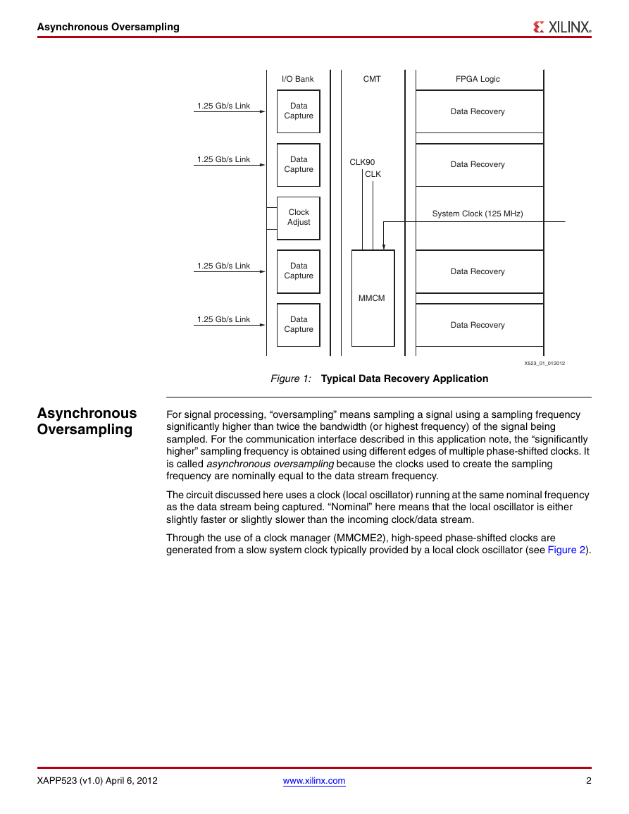
actually recovered, but the arriving data is fully extracted. Figure 1 shows a typical use case.
© Copyright 2012 Xilinx, Inc. Xilinx, the Xilinx logo, Artix, ISE, Kintex, Spartan, Virtex, Zynq, and other designated brands included herein are trademarks of Xilinx in the United
States and other countries. All other trademarks are the property of their respective owners.
XAPP523 (v1.0) April 6, 2012
www.xilinx.com
1
�
Asynchronous Oversampling
X-Ref Target - Figure 1
I/O Bank
CMT
FPGA Logic
1.25 Gb/s Link
1.25 Gb/s Link
1.25 Gb/s Link
1.25 Gb/s Link
Data
Capture
Data
Capture
Clock
Adjust
Data
Capture
Data
Capture
Data Recovery
CLK90
CLK
Data Recovery
System Clock (125 MHz)
MMCM
Data Recovery
Data Recovery
Asynchronous
Oversampling
Figure 1: Typical Data Recovery Application
X523_01_012012
For signal processing, “oversampling” means sampling a signal using a sampling frequency
significantly higher than twice the bandwidth (or highest frequency) of the signal being
sampled. For the communication interface described in this application note, the “significantly
higher” sampling frequency is obtained using different edges of multiple phase-shifted clocks. It
is called asynchronous oversampling because the clocks used to create the sampling
frequency are nominally equal to the data stream frequency.
The circuit discussed here uses a clock (local oscillator) running at the same nominal frequency
as the data stream being captured. “Nominal” here means that the local oscillator is either
slightly faster or slightly slower than the incoming clock/data stream.
Through the use of a clock manager (MMCME2), high-speed phase-shifted clocks are
generated from a slow system clock typically provided by a local clock oscillator (see Figure 2).
XAPP523 (v1.0) April 6, 2012
www.xilinx.com
2
�
Asynchronous Oversampling
X-Ref Target - Figure 2
n
i
S
E
D
R
E
S
I
l
l
A
o
T
e
d
o
M
E
L
P
M
A
S
R
E
V
O
BUFIO
BUFIO
BUFG
CLK
CLK90
IntClk
BUFG
IntClkDiv
MMCM
Pattern
S
E
D
R
E
S
O
S
E
D
R
E
S
I
State
Machine
125 MHz
To All Clocked FPGA
Logic in this Clock Area
To Data Recovery
Logic in this Clock Area
Figure 2: Clock Generation Using MMCME2
X523_02_012512
The function of the two extra clocks and ISERDES/OSERDES combination shown in Figure 2
is explained in Clocking and Data Flow, page 10. The generated CLK and CLK90 clocks make
it possible to oversample an incoming data stream on four edges, meaning that each bit of the
DDR data stream can be sampled twice, as shown in Figure 3.
X-Ref Target - Figure 3
0
90
180
270
CLK
CLK90
Different
positions of
the data with
respect to the
clocks.
Figure 3: Data Oversampling on Four Clock Edges
Two Data Sample Edges Per Bit
X523_03_012012
If the incoming data stream is split into two branches and one branch is delayed by 45°, it is
possible to 4x oversample every data bit. The details of how this circuit is constructed using
MMCME2, IODELAYE2, and ISERDESE2 is shown in Figure 4.
XAPP523 (v1.0) April 6, 2012
www.xilinx.com
3
�
Asynchronous Oversampling
X-Ref Target - Figure 4
BUFIO
BUFIO
CLK
CLK90
CLKIN
BUFG
IntClk
MMCM
BUFG
IntClkDiv
Data Recovery Unit
IBUFDS_DIFF_OUT
IDELAY
0 Shift
IDELAY
45 Shift
S
E
D
R
E
S
I
S
E
D
R
E
S
I
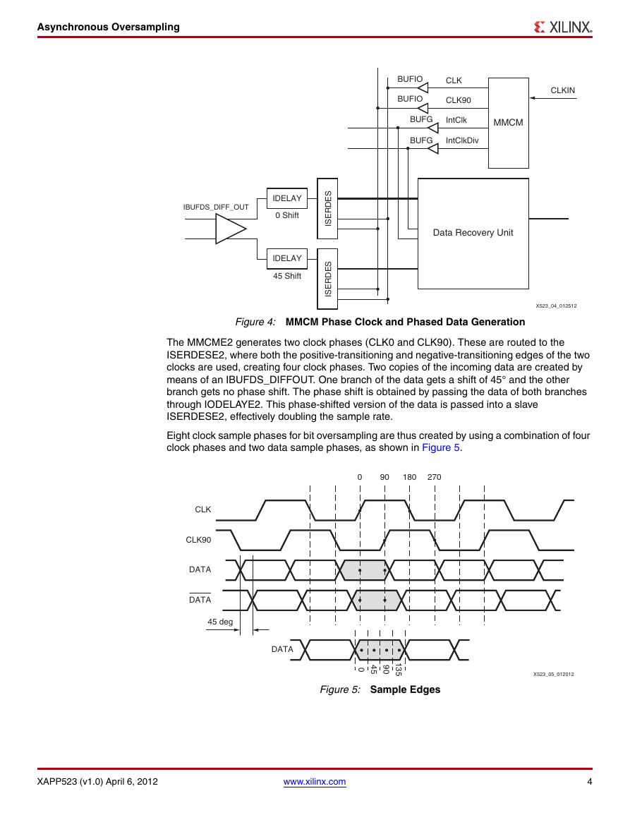
Figure 4: MMCM Phase Clock and Phased Data Generation
X523_04_012512
The MMCME2 generates two clock phases (CLK0 and CLK90). These are routed to the
ISERDESE2, where both the positive-transitioning and negative-transitioning edges of the two
clocks are used, creating four clock phases. Two copies of the incoming data are created by
means of an IBUFDS_DIFFOUT. One branch of the data gets a shift of 45° and the other
branch gets no phase shift. The phase shift is obtained by passing the data of both branches
through IODELAYE2. This phase-shifted version of the data is passed into a slave
ISERDESE2, effectively doubling the sample rate.
Eight clock sample phases for bit oversampling are thus created by using a combination of four
clock phases and two data sample phases, as shown in Figure 5.
0
90
180
270
X-Ref Target - Figure 5
CLK
CLK90
DATA
DATA
45 deg
DATA
0
4
5
9
0
1
3
5
Figure 5: Sample Edges
X523_05_012012
XAPP523 (v1.0) April 6, 2012
www.xilinx.com
4
�
7 Series ISERDESE2 Oversampling Mode
IDELAY Tap Setting Calculation Example
The following list outlines the logical flow of timing assumptions and calculations leading to the
IDELAY tap settings:
1. Assume that the incoming data stream runs at 1.25 Gb/s; the bit time is therefore 800 ps.
2. The CLK and CLK90 clocks therefore run at 625 MHz, or 1.6 ns.
3. The edges of both clocks arriving at 0°, 90°, 180°, and 270° have positions at 0, 400, 800,
and 1200 ps.
4. To shift 45°, one branch of the data must be delayed by 200 ps.
5. The tap delay of an IDELAY component is controlled by an IDELAYCTRL component. The
IDELAYCTRL component in this design is clocked at 310 MHz, so a single-tap delay is
52 ps. (Refer to Note 1 in the Input/Output Delay Switching Characteristics table in DS182,
Kintex-7 FPGAs Data Sheet: DC and Switching Characteristics.)
6. The 200 ps desired delay for 45° phase shift is divided by 52 ps per tap to give 3.8 or
4 taps.
Therefore, the IDELAY_VALUE of the first IDELAY must be set to 0, and the IDELAY_VALUE of
the second (slave) IDELAY must be set to 4.
The ISERDESE2 component in 7 series FPGAs is an improved version of similar components
in previous FPGA families (ISERDES in Virtex-5 FPGAs and ISERDESE1 in Virtex-6 FPGAs).
The ISERDESE2 component can implement (i.e., be configured as) different functions:
In its most basic function, the ISERDESE2 provides the functionality of an IDDR flip-flop.
A second and more complex function is that of a dedicated serial-to-parallel converter with
specific clocking and logic features designed to facilitate the implementation of high-speed
source-synchronous applications (NETWORKING mode).
A third function is MEMORY mode, where the ISERDES is configured as a dedicated
interface for different types of memories (QDR, DDR3, etc.).
In its fourth and final function, the ISERDESE2 can be used in OVERSAMPLING mode.
Here, ISERDESE2 is used to capture two phases of DDR data. In this mode, the
ISERDESE2 is thus used as a dual set of IDDR flip-flops.
For detailed descriptions of the ISERDESE2 functionality, see UG471, 7 Series FPGAs
SelectIO Resources User Guide.
For convenience, Figure 6 shows the ISERDESE2, with oversampling mode configuration. In
earlier implementations, the oversampling design was implemented in FPGA logic using SLICE
flip-flops. With 7 series FPGAs, this functionality is implemented in the ISERDESE2.
7 Series
ISERDESE2
Oversampling
Mode
XAPP523 (v1.0) April 6, 2012
www.xilinx.com
5
�
7 Series ISERDESE2 Oversampling Mode
X-Ref Target - Figure 6
INTERFACE_TYPE : string := “OVERSAMPLE”;
SERDES_MODE : string := “MASTER”;
DATA_WIDTH : interger := 4;
DATA_RATE : string := “DDR”;
OFB_USED : string := “FALSE”;
IOBDELAY : string := “IFD”;
NUM_CE : integer := 1;
DYN_CLKDIV_INV_EN : string := “FALSE”;
DYN_CLK_INV_EN : string := “FALSE”;
INIT_Q1 : bit := ‘0’;
INIT_Q2 : bit := ‘0’;
INIT_Q3 : bit := ‘0’;
INIT_Q4 : bit := ‘0’;
SRVAL_Q1 : bit := ‘0’;
SRVAL_Q2 : bit := ‘0’;
SRVAL_Q3 : bit := ‘0’;
SRVAL_Q4 : bit := ‘0’;
SHIFTOUT1
SHIFTOUT2
O
Q1
Q2
Q3
Q4
Q5
Q6
Q7
Q8
SHIFTIN1
SHIFTIN2
OFB
D
DDLY
CE1
CE2
RST
BITSLIP
CLK
CLKB
CLKDIV
CLKDIVP
DYNCLKDIVSEL
DYNCLKSEL
OCLK
OCLKB
ISERDESE2
DDLY
CLK
CLKB
OCLK
OCLKB
QD
QD
QD
QD
QD
QD
QD
QD
QD
Q1
Q2
Q3
QD
QD
Q4
QD
Figure 6:
ISERDESE2 in OVERSAMPLING Mode Configuration
X523_15_021012
Data Recovery Unit
An ISERDESE2 used in networking mode requires a high-speed sampling clock (CLK) to
capture the serial data stream in the ISERDESE2. It also needs a low-speed function of CLK
(CLKDIV) to present the captured data in parallel format at the outputs of the ISERDESE2. The
internal circuits in the ISERDESE2 ensure that this conversion from the CLK level to the
CLKDIV level works as a clock-domain crossing (CDC) circuit.
The output of the ISERDESE2 components in oversampling mode is generated from the
high-speed sampling clocks (CLK/CLKB and OCLK/OCLKB). These clocks are only available
for clocking of ISERDESE2 and/or OSERDESE2.
The CDC operation must thus be implemented in registers in the FPGA logic. The details of
how this is done are discussed in Clocking and Data Flow, page 10. The CDC registers and
some comparing logic are implemented in the data recovery unit (DRU) and are clocked by the
CLK input. The low-speed clock (CLKP or CLKDIV) clocks the rest of the DRU.
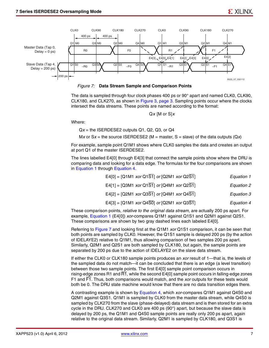
The locations of the sampling and comparison points relative to the data stream coming into the
FPGA are shown in Figure 7. There are two streams of data, one offset from the other by
200 ps (4 IDELAY taps). For this application, the speed of the arriving data stream is1.25 Gb/s.
Through use of the IBUFDS_DIFFOUT primitive, one data stream is the complement of the
other data stream, similar to the input data of IBUFDS_DIFF_OUT (i.e., differential signaling).
XAPP523 (v1.0) April 6, 2012
www.xilinx.com
6
�
7 Series ISERDESE2 Oversampling Mode
X-Ref Target - Figure 7
Master Data (Tap 0,
Delay = 0 ps)
Slave Data (Tap 4,
Delay = 200 ps)
200 ps
CLK0
CLK90
CLK180
CLK270
CLK0
CLK90
CLK180
CLK270
400 ps
400 ps
Q1
M0
Q3
M0
Q2
M0
Q4
M0
Q1
M1
Q3
M1
Q2
M1
Q4
M1
R0
F0
R1
F1
Q1
S0
~R0
Q3
S0
Q2
S0
Q4
S0
~F0
Q1
S1
~R1
Q3
S1
Q2
S1
~F1
E4[3] E4[0] E4[1]
E4[2] E4[3]
E4[0]
E4[2]
Q4
S1
X523_07_032112
Figure 7: Data Stream Sample and Comparison Points
The data is sampled through four clock phases 400 ps or 90° apart and named CLK0, CLK90,
CLK180, and CLK270, as shown in Figure 3, page 3. Sampling points occur where the clocks
intersect the data streams. These points are named according to the format:
Where:
Qx [M or S]x
Qx = the ISERDESE2 outputs Q1, Q2, Q3, or Q4
Mx or Sx = the source ISERDESE2 (M = master, S = slave) of the data outputs (Qx)
For example, sample point Q1M1 shows where CLK0 samples the data and creates an output
at port Q1 of the master ISERDESE2.
The lines labelled E4[0] through E4[3] that connect the sample points show where the DRU is
comparing data and looking for a data edge. The formulas for the four comparisons are shown
in Equation 1 through Equation 4.
E4[0] = [Q1M1 xor Q1S1] or [Q2M1 xor Q2S1]
E4[1] = [Q3M1 xor Q1S1] or [Q4M1 xor Q2S1]
E4[2] = [Q2M1 xor Q3S1] or [Q4M1 xor Q4S1]
E4[3] = [Q1M1 xor Q4S0] or [Q2M1 xor Q3S1]
Equation 1
Equation 2
Equation 3
Equation 4
These comparison points, relative to the original data stream, are actually 200 ps apart. For
example, Equation 1 (E4[0]) xor-compares Q1M1 against Q1S1 and Q2M1 against Q2S1.
These comparisons are shown by two gray dashed lines each labeled E4[0].
Referring to Figure 7 and looking first at the Q1M1 xor Q1S1 comparison, it can be seen that
both points are sampled by CLK0. However, the Q1S1 sample is delayed 200 ps (by the action
of IDELAYE2) relative to Q1M1, thus allowing comparison of two samples 200 ps apart.
Similarly, Q2M1 and Q2S1 are both sampled by CLK180, but again, the sample points are
separated by 200 ps due to the action of IDELAYE2 on the slave data stream.
If either the CLK0 or CLK180 sample points produces an xor result of 1—that is, the levels of
the sampled data do not match—it can be concluded that there is an edge (a level transition)
between those two sample points. The first E4[0] sample point comparison occurs in
rising-edge zones R1 and R1, while the second E4[0] sample point occurs in falling-edge zones
F1 and F1. Thus, both comparisons would match, and the xor outputs for these tests would
both be 0. The DRU state machine would know that there are no data transition edges there.
A contrasting example is shown by Equation 4, which xor-compares Q1M1 against Q4S0 and
Q2M1 against Q3S1. Q1M1 is sampled by CLK0 from the master data stream, while Q4S0 is
sampled by CLK270 from the slave (phase-delayed) data stream and is then stored for an extra
cycle in the DRU. CLK270 and CLK0 are 400 ps (90°) apart, but because the slave data is
delayed by 200 ps, the Q1M1 and Q4S0 sample points are really only 200 ps apart, again
relative to the original data stream. Similarly, Q2M1 is sampled by CLK180, and Q3S1 is
XAPP523 (v1.0) April 6, 2012
www.xilinx.com
7
�
7 Series ISERDESE2 Oversampling Mode
sampled by CLK90. Again, the sample points are 200 ps apart relative to the original data
stream. For each comparison, one sample point falls in a rising-edge zone and the other falls in
a falling-edge zone. These two comparisons would produce an xor result of 1, indicating that an
edge (level transition) exists somewhere between the two sample points in each comparison.
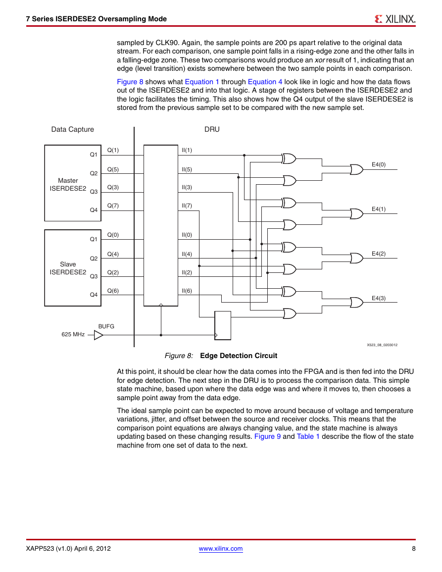
Figure 8 shows what Equation 1 through Equation 4 look like in logic and how the data flows
out of the ISERDESE2 and into that logic. A stage of registers between the ISERDESE2 and
the logic facilitates the timing. This also shows how the Q4 output of the slave ISERDESE2 is
stored from the previous sample set to be compared with the new sample set.
X-Ref Target - Figure 8
Data Capture
DRU
Master
ISERDESE2
Slave
ISERDESE2
Q(1)
Q(5)
Q(3)
Q(7)
Q(0)
Q(4)
Q(2)
Q(6)
Q1
Q2
Q3
Q4
Q1
Q2
Q3
Q4
BUFG
625 MHz
II(1)
II(5)
II(3)
II(7)
II(0)
II(4)
II(2)
II(6)
E4(0)
E4(1)
E4(2)
E4(3)
Figure 8: Edge Detection Circuit
X523_08_0203012
At this point, it should be clear how the data comes into the FPGA and is then fed into the DRU
for edge detection. The next step in the DRU is to process the comparison data. This simple
state machine, based upon where the data edge was and where it moves to, then chooses a
sample point away from the data edge.
The ideal sample point can be expected to move around because of voltage and temperature
variations, jitter, and offset between the source and receiver clocks. This means that the
comparison point equations are always changing value, and the state machine is always
updating based on these changing results. Figure 9 and Table 1 describe the flow of the state
machine from one set of data to the next.
XAPP523 (v1.0) April 6, 2012
www.xilinx.com
8
�




 2023年江西萍乡中考道德与法治真题及答案.doc
 2012年重庆南川中考生物真题及答案.doc
 2013年江西师范大学地理学综合及文艺理论基础考研真题.doc
 2020年四川甘孜小升初语文真题及答案I卷.doc
 2020年注册岩土工程师专业基础考试真题及答案.doc
 2023-2024学年福建省厦门市九年级上学期数学月考试题及答案.doc
 2021-2022学年辽宁省沈阳市大东区九年级上学期语文期末试题及答案.doc
 2022-2023学年北京东城区初三第一学期物理期末试卷及答案.doc
 2018上半年江西教师资格初中地理学科知识与教学能力真题及答案.doc
 2012年河北国家公务员申论考试真题及答案-省级.doc
 2020-2021学年江苏省扬州市江都区邵樊片九年级上学期数学第一次质量检测试题及答案.doc
 2022下半年黑龙江教师资格证中学综合素质真题及答案.doc